
 Open Access Article
 This Open Access Article is licensed under a
 Creative Commons Attribution 3.0 Unported Licence
Electroluminescence in a rectifying graphene/InGaN junction
Hak Dong Choa,
Im Taek Yoona,
Sh. U. Yuldashevb,
Tae Won Kangab,
Deuk Young Kim*ac and
Jong-Kwon Lee *d
*d
aQuantum Functional Semiconductor Research Center, Dongguk University, Seoul 04620, Republic of Korea. E-mail: dykim@dongguk.edu
bNano Information Technology Academy, Dongguk University, Seoul 04620, Republic of Korea
cDivision of Physics and Semiconductor Science, Dongguk University, Seoul 04620, Republic of Korea
dDepartment of Nanostructure Technology, National NanoFab Center, Daejeon 34141, Republic of Korea. E-mail: jklee7@msn.com
First published on 1st November 2017
Abstract
A graphene-InGaN Schottky junction has been successfully fabricated by transferring graphene layers onto n-type In0.23Ga0.77N/GaN/Al2O3 substrates. Current–voltage (I–V) measurement across the junction demonstrates the rectifying behaviour. Temperature dependent I–V characteristics in a range of 10 K to 300 K reveal that the charge transport mechanism is dominated by thermionic emission. Also, it is observed that the charge-transfer induced variation of Fermi energy of graphene affects the flow of current. This graphene/InGaN junction shows electroluminescence (EL) characteristics under a forward bias, producing bright blue emission (430 nm) at room temperature. As the temperature increases, the EL peak is shifted to a lower energy with a reduced peak intensity due to the increased nonradiative recombination rate. The dependence of EL intensity on the current of the graphene/InGaN junction confirms the band-to-band recombination mechanism in the InGaN layer by the bimolecular radiative recombination. Therefore, the observed results provide an insight for implementing graphene based Schottky-junction devices with tunable emission by utilizing the variable bandgap of the InGaN layer.
Introduction
Graphene, a two-dimensional hexagonal lattice of sp2 hybridized carbon atoms, shows outstanding electrical, optical, chemical and thermomechanical properties.1–5 Thus, it has been extensively studied for integration with the current semiconductor technologies to realize next-generation electronic and photonic devices.6–10 Especially, the graphene/semiconductor junction is one of the simplest devices in graphene embedded semiconductor technology with its tunable Schottky-barrier height. Also, the graphene/semiconductor junction is a suitable platform for the study of interface transport mechanisms, and the development of its fabrication process is crucial to realize graphene integrated devices such as photo-detection, high-speed communications, solar cells and sensors. Therefore, a lot of efforts have been made to study the graphene–semiconductor contacts such as graphene–Si, graphene–GaAs and graphene–GaN for high performance light-emitting diode (LED), photo-detector and solar cell applications.11–16Indium Gallium Nitride (InGaN) ternary alloy has attracted much attention for realizing high efficiency photonic devices including solar cells and LEDs because its bandgap covers the whole solar spectrum by changing its In composition.17 Also, the InGaN material has a high absorption coefficient18 and a good radiation tolerance.19 However, the high residual donors' concentration and the lack of ad. hoc. acceptors20 make its p-doing difficult. Moreover, it is difficult to fabricate high quality p-doped InGaN layer because of the complex technological processes, as well as to realize ohmic contacts with electrodes of various devices.
In this study, therefore, we have successfully fabricated graphene/InGaN Schottky junction by transferring single layer graphene onto n-doped InGaN layer. Then, the fabricated devices were characterized by Raman spectroscopy, Hall effect and temperature dependent I–V measurements, as well as the current-dependent and temperature-dependent electro-luminescence (EL) measurements. The devices show rectifying diode behaviour with an estimated Schottky barrier energy of ∼0.34 eV, producing blue emission at a wavelength of 430 nm at room temperature. It is observed that the EL emission is related to the band-to-band recombination mechanism in the InGaN layer by the bimolecular radiative recombination.
Experimental section
Device fabrication
The growth of InGaN films on the aluminium-oxide (Al2O3) substrate was performed in a conventional low pressure metal–organic chemical-vapor deposition (MOCVD) system at a pressure of 540 mbar. Purified hydrogen and nitrogen were used as carrier gases. Silane gas was used for n-type doping. The growth process began with heating the Al2O3 substrate in an ambient of ammonia and hydrogen. Once a stable temperature was established, growth of 45 nm thick gallium nitride (GaN) buffer layer at 450 °C and 300 nm thick InGaN![[thin space (1/6-em)]](https://www.rsc.org/images/entities/char_2009.gif) :Si layers at 750 °C were performed, respectively. Then, the structure was completed with n-InGaN/GaN/Al2O3 (0001) as shown in Fig. 1.
:Si layers at 750 °C were performed, respectively. Then, the structure was completed with n-InGaN/GaN/Al2O3 (0001) as shown in Fig. 1.
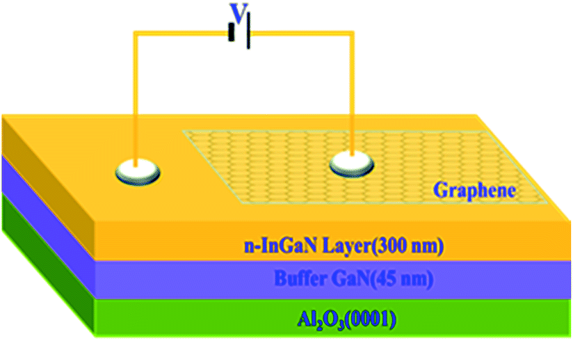 | ||
| Fig. 1 Schematic of the fabricated device by transferring a graphene layer on top of the In0.23Ga0.77N/GaN/Al2O3 substrate. | ||
For the fabrication of Schottky didoes, the graphene formed on 25-μm thick Cu foil by the CVD method was transferred onto the n-InGaN layer by using polymethyl methacrylate (PMMA) sacrificial layer. Here the transfer process of graphene on to the substrate is similar to that reported in the literatures.21 Then, the PMMA was removed by acetone in an ultrasonic bath for 20 min, leaving the single layer graphene onto the n-InGaN layer. The transferred graphene was then rinsed in a 30% HCl solution at 60 °C for 30 min to remove residual Fe+3 ions. As a result, the graphene layer with a low defect density was prepared on the n-InGaN/GaN/Al2O3 substrate. Finally, we adopted silver pastes to make an intimate contact with graphene as an anode as well as a contact with n-InGaN layer as a cathode as schematically illustrated in Fig. 1.
Device characterization
Graphene layers transferred on the InGaN/GaN/Al2O3 substrate were identified by using micro-Raman spectroscopy with 514 nm excitation. The surface topology of InGaN layer was probed by atomic force microscopy (AFM) in a tapping mode. Its resistivity and doping concentration were investigated by using a Hall effect measurement system at room temperature with a magnetic field of ∼0.5 Tesla. I–V measurements were taken in darkroom conditions using a Keithley 6430 sub fempto amp source-meter, by changing the temperature from 10 K to 300 K. The EL signals from the samples placed in a He closed-cycle cryostat were detected a photomultiplier tube behind the SPEX spectrometer equipped with a 0.75 m grating monochromator. An electric bias of 5 V was applied to measure the temperature dependence of the electroluminescence spectra of the graphene/InGaN junction, and the EL spectra at 10 K were characterized with varying the current density.Results and discussion
Fig. 2a shows the surface morphology of n-InGaN layer deposited on the GaN/Al2O3 substrate. The measured RMS value of roughness for InGaN layer is about 0.29 nm, revealing a good surface topography. Also, the resistivity and the mobility of the n-InGaN layer estimated by Hall effect measurement are 0.00934 ohm-cm and 85.7 cm2 v−1 s−1, respectively. The measured doping concentration of n-InGaN layer is 7.8 × 10¹⁸, demonstrating heavily n-doped InGaN. The synthesized graphene layer on SiO2/Si substrate was characterized by Raman spectroscopy as shown in Fig. 2c. Here, the Raman spectrum for graphene clearly shows the G (∼1596 cm−1) and 2D (∼2710 cm−1) bands with the negligible D band near 1350 cm−1, which verifies that the synthesized graphene is a high quality layer. Also, a single graphene layer was identified by the peak intensity ratio of the 2D band to the G band greater than one, and the full width at half maximum of 2D peak less than 40 cm−1. The presence of extrinsic residual doping in a CVD graphene is attributed to residual water vapor or oxygen in an environment.22 For our synthesized graphene, the presence of the residual impurity moves the Fermi-level (EF) of graphene lowering below the Dirac point, which leads to a proper hole doping of the graphene.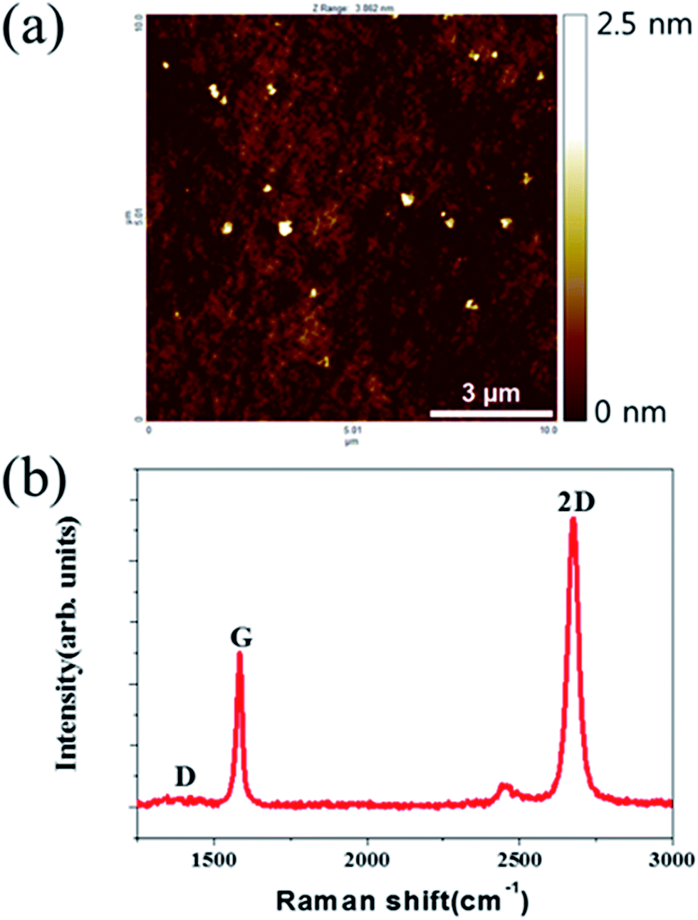 | ||
| Fig. 2 (a) AFM image of the In0.23Ga0.77N layer deposited on the GaN/Al2O3 substrate. (b) Raman spectrum of the synthesis graphene transferred on a SiO2/Si substrate. | ||
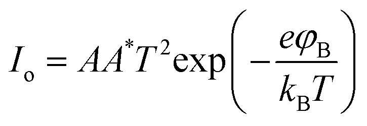
Due to the difference of EF between graphene and n-doped InGaN layer, the Schottky barrier (φB) is generated in between them. Since the graphene and the InGaN layer adhere to each other in an intimate van-der-Waals contact, it is expected to pass current in the forward bias when the InGaN layer is negatively biased, while becoming resistive in the reverse bias when the InGaN layer is positively biased. At the forward bias the EF in InGaN is shifted up and the effective φB decreases, whereas at the reverse bias the EF in InGaN is shifted down and the φB increases as illustrated in Fig. 3a. The I–V data measured in the temperature range from 10 K to 300 K exhibit clearly rectification behaviour as seen in Fig. 3b. As temperature increases from 10 K to 300 K, the current level at a forward bias of 5 V gradually increases from 97.0 μA to 180.3 μA. The rectifying ratio23,24 at ±5 V is 7.4 at 10 K and 3.9 at 300 K, respectively. The estimated rectifying ratio is much lower comparing with the value of p–n junctions because the φB is much lower than that for p–n junction. With increasing temperature the kinetic energy of electrons increases and the number of the carriers which can overcome the φB increases. The electron transport over the φB at the metal–semiconductor interface is described by thermionic-emission theory with the following equations
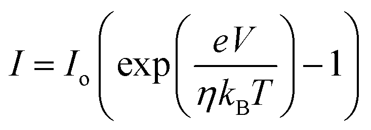 | (1) |
 | (2) |
26 and electron affinity of InGaN with 23% of In is about 4.2 eV,27 the φB obtained from the I–V characteristic is in agreement with its value given in literature. It is noted that the φB does not change much with temperature, while with increasing temperature the kinetic energy of electrons increases and the thermal emission of electrons through barrier increases. Meanwhile, since the EF of graphene is changed during charge transfer,28,29 the φB at high bias levels can be varied. Especially, this variation at a high reverse bias results in increased leakage currents because the induced negative charge in the graphene is enough to increase the EF of graphene.
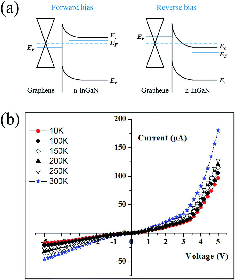 | ||
| Fig. 3 (a) Schottky-band diagrams of graphene/InGaN junction under forward bias and reverse bias cases. (b) Current–voltage characteristics of the graphene/InGaN junction measured at various temperature ranges from 10 K to 300 K. | ||
Fig. 4a shows the EL spectra of InGaN/graphene heterostructure measured at different temperature ranging from 10 K to 350 K at the electric bias of 5 V. There is a main EL peak at around 2.84 eV (430 nm) at 300 K for the investigated Schottky-type light-emitting devices, corresponding to the emission from the n-In0.23Ga0.77N at In mole fraction of 0.23. Thus, it is observed that the holes injected from graphene are effectively recombined with the electrons accumulated in the n-InGaN layer. Also, as the temperature increases, the EL peak position is shifted to a lower energy or longer wavelength (red-shift), which is attributed to the bandgap lowering. Meanwhile, the EL intensity decreases even so the current passing through the device increases with increasing temperature at the fixed voltage bias. Here, it is noted that the radiative recombination rate is usually assumed to be independent on temperature, whereas the nonradiative recombination rate increases due to thermal activation of nonradiative recombination centers. The inset of Fig. 4a shows the photograph of InGaN/graphene device under forward biasing. The bright blue light emission is clearly seen with the naked eye. Fig. 4b shows the EL spectra measured for different currents of 45, 70, 97 μA passing through the device at 10 K. The inset of Fig. 4b shows the dependence of EL intensity on the current in a double logarithmic scale. The slope of this dependence is close to 2, which demonstrates the bimolecular radiative recombination rate. Thus, this observation confirms the EL emission is related to the band-to-band recombination mechanism in the InGaN layer.
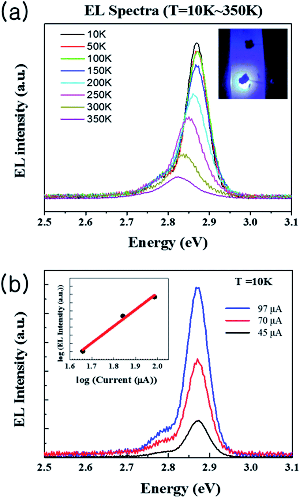 | ||
| Fig. 4 Electroluminescence spectra of the graphene/In0.23Ga0.77N junction (a) at various temperatures ranging from 10 K to 350 K and (b) at various drive current levels at 10 K. | ||
The relationship between band gap energy and temperature is usually described by Varshni's empirical equation30
 | (3) |
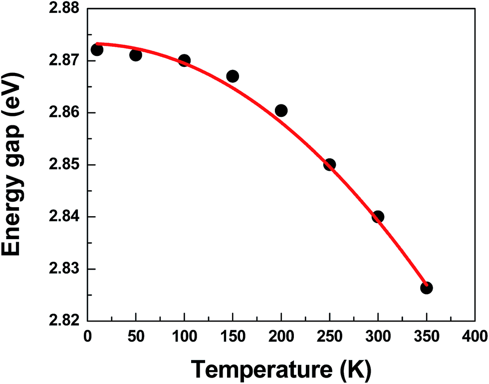 | ||
| Fig. 5 Temperature dependence of the electroluminescence peak maximum shown by filed circles and solid curve shows the result of fitting by using Varshni's eqn (3). | ||
The emitting wavelength of this graphene/InGaN junction device can be easily regulated by utilizing a feature of tunable band edge in n-InGaN depending on In concentration. For example, while the energy gap of used InGaN with 23% of In is of 2.84 eV at room temperature, we can utilize this graphene–InGaN heterostructure to develop promising near-infrared nano devices by adopting the InGaN with much higher concentration of In. Here, the In concentration in InGaN alloy regulates its energy gap, as much higher the In concentration the lower energy gap of InGaN. The donor states were produced by Si doping which is very popular donor dopant for InGaN with small activation energy of about 17 meV, providing very high concentration of electrons in InGaN. In addition, the hole-doping concentration of graphene layer contacted with n-type semiconductor layer can be tuned to build suitable φB, as well as to make an ohmic contact with an anode electrode. Therefore, the suggested graphene/InGaN junction is expected to be a promising structure to realize wavelength tuning of light–emitting devices with a tunable φB in a broad wavelength range, which is a distinctive feature in comparison with other types of graphene/semiconductor junction LEDs.
Conclusions
We developed the graphene/InGaN Schottky-junction light-emitting device, and demonstrated its EL characteristics with a peak wavelength of 430 nm at room temperature. The EL peak shift to a longer wavelength with a reduced intensity is mainly attributed to the enhanced non-radiative recombination rate with increasing temperature. The current-dependent EL characteristics exhibited that this EL is originated from the band-to-band recombination mechanism in the InGaN layer. The presented graphene/InGaN junction can be a promising structure for realizing Schottky-junction based light-emitting devices with a tunable emission peak.Conflicts of interest
There are no conflicts to declare.Acknowledgements
This research was partially supported by Basic Science Research Program through the National Research Foundation of Korea funded by the Ministry of Education (2017R1D1A1B03034672), (2016R1A6A1A03012877), (2017R1D1A1B03032759), (2016R1D1A1B03930992), (2014R1A2A1A12066298). Also, we would like to acknowledge the financial sup-port from the R&D Convergence Program of National Research Council of Science & Technology of Republic of Korea (CAP-16-10-KIMS).Notes and references
- A. K. Geim, Science, 2009, 324, 1530 CrossRef CAS PubMed.
- Y. Zhu, S. Murali, W. Cai, X. Li, J. W. Suk, J. R. Potts and R. S. Ruoff, Adv. Mater., 2010, 22, 3906 CrossRef CAS PubMed.
- J.-K. Lee, S. Yamazaki, H. Yun, J. Park, G. P. Kennedy, G.-T. Kim, O. Pietzsch, R. Wisendanger, S. Lee, S. Hong, U. Dettlaff-Weglikowska and S. Roth, Nano Lett., 2013, 13, 3494 CrossRef CAS PubMed.
- B. Davaji, H. D. Cho, M. Malakoutian, J.-K. Lee, G. Panin, T. W. Kang and C. H. Lee, Sci. Rep., 2017, 7, 8811 CrossRef PubMed.
- J. D. Fowler, M. J. Allen, V. C. Tung, Y. Yang, R. B. Kaner and B. H. Weiller, ACS Nano, 2009, 3, 301 CrossRef CAS PubMed.
- K. S. Novoselov, V. I. Fal'ko, L. Colombo, P. R. Gellert, M. G. Schwab and K. Kim, Nature, 2012, 490, 192 CrossRef CAS PubMed.
- Q. Bao and K. P. Loh, ACS Nano, 2012, 6, 3677 CrossRef CAS PubMed.
- J.-K. Lee, H. Sung, M. S. Jang, H. Yoon and M. Choi, J. Mater. Chem. C, 2015, 3, 8275 RSC.
- C.-C. Chen, M. Aykol, C.-C. Chang, A. F. J. Levi and S. B. Cronin, Nano Lett., 2011, 11, 1863 CrossRef CAS PubMed.
- Y.-M. Lin, A. Valdes-Garcia, S.-J. Han, D. B. Farmer, I. Meric, Y. Sun, Y. Wu, C. Dimitrakopoulos, A. Grill, P. Avouris and K. A. Jenkins, Science, 2011, 332, 1294 CrossRef CAS PubMed.
- F. Bonaccorso, Z. Sun, T. Hasan and A. C. Ferrari, Nat. Photonics, 2010, 4, 611 CrossRef CAS.
- G. Kalita, K. Wakita, M. Umeno and M. Tanemura, Phys. Status Solidi RRL, 2013, 7, 340 CrossRef CAS.
- X. Li, W. Chen, S. Zhang, Z. Wu, P. Wang, Z. Xu, H. Chen, W. Yin, H. Zhong and S. Lin, Nano Energy, 2015, 16, 310 CrossRef CAS.
- F. Lin, S.-W. Chen, J. Meng, G. Tse, X.-W. Fu, B. Shen, Z.-M. Liao and D.-P. Yu, Appl. Phys. Lett., 2014, 105, 073103 CrossRef.
- X. Li, H. Zhu, K. Wang, A. Cao, J. Wei, C. Li, Y. Jia, Z. Li, X. Li and D. Wu, Adv. Mater., 2010, 22, 2743 CrossRef CAS PubMed.
- Z. Yin, J. Zhu, Q. He, X. Cao, C. Tan, H. Chen, Q. Yan and H. Zhang, Adv. Energy Mater., 2014, 4, 1300574 CrossRef.
- A. Bhuiyan, K. Sugita, A. Hashimoto and A. Yamamoto, IEEE J. Photovolt., 2011, 2, 276 CrossRef.
- S. Lin, S. Zeng, X. Cai, J. Zhang, S. Wu, L. Sun and B. Zhang, J. Mater. Sci., 2012, 47, 4595 CrossRef CAS.
- A. Y. Polyakov, S. Pearton, P. Frenzer, F. Ren, L. Liu and J. Kim, J. Mater. Chem. C, 2013, 1, 877 RSC.
- R. Dahal, B. Pantha, J. Li, J. Lin and H. Jiang, Appl. Phys. Lett., 2009, 94, 063505 CrossRef.
- J. W. Suk, W. H. Lee, J. Lee, H. Chou, R. D. Piner, Y. Hao, D. Akinwande and R. S. Ruoff, Nano Lett., 2013, 13, 1462 CrossRef CAS PubMed.
- P. Joshi, H. E. Romero, A. T. Neal, V. K. Toutam and S. A. Tadigadapa, J. Phys.: Condens. Matter, 2010, 22, 334214 CrossRef CAS PubMed.
- J. Zeng, K.-Q. Chen, J. He, X.-J. Zhang and C. Q. Sun, J. Phys. Chem. C, 2011, 115, 25072 CAS.
- Y.-C. Ling, F. Ning, Y.-h. Zhou and K.-Q. Chen, Org. Electron., 2015, 19, 92 CrossRef CAS.
- E. Arslan, H. Cakmak and E. Ozbay, Microelectron. Eng., 2012, 100, 51 CrossRef CAS.
- R. Yan, Q. Zhang, W. Li, I. Calizo, T. Shen, C. A. Richter, A. R. Hight-Walker, X. Liang, A. Seabaugh, D. Jena, H. G. Xing, D. J. Gundlach and N. V. Nguyen, Appl. Phys. Lett., 2012, 101, 022105 CrossRef.
- M. E. Levinshtein, S. L. Rumyantsev and M. S. Shur, Properties of Advanced Semiconductor Materials: GaN, AlN, InN, BN, SiC, SiGe, John Wiley & Sons, Inc., New York, 2001, pp. 1–30 Search PubMed.
- A. Das, S. Pisana, B. Chakraborty, S. Piscanec, S. K. Saha, U. V. Waghmare, K. S. Novoselov, H. R. Krishnamurthy, A. K. Geim, A. C. Ferrari and A. K. Sood, Nat. Nanotechnol., 2008, 3, 210 CrossRef CAS PubMed.
- Y. J. Yu, Y. Zhao, S. Ryu, L. E. Brus, K. S. Kim and P. Kim, Nano Lett., 2009, 9, 3430 CrossRef CAS PubMed.
- Y. P. Varshni, Physica, 1967, 34, 149 CrossRef CAS.
| This journal is © The Royal Society of Chemistry 2017 |