
 Open Access Article
 This Open Access Article is licensed under a Creative Commons Attribution-Non Commercial 3.0 Unported Licence
A simple synthesis of Ga2O3 and GaN nanocrystals†
Erwei Huanga,
Juxia Lia,
Guangjun Wua,
Weili Dai a,
Naijia Guanab and
Landong Li*ab
a,
Naijia Guanab and
Landong Li*ab
aSchool of Materials Science and Engineering, National Institute for Advanced Materials, Nankai University, Tianjin, 300350, P. R. China
bKey Laboratory of Advanced Energy Materials Chemistry (Ministry of Education), Collaborative Innovation Center of Chemical Science and Engineering, Tianjin, 300071, P. R. China. E-mail: lild@nankai.edu.cn
First published on 12th October 2017
Abstract
The synthesis of gallium oxide and nitride nanocrystals is challenging. Herein, a forced hydrolysis route is developed to synthesize α-GaOOH and the morphology control of nanocrystals is realized by adjusting the ratios of ionic strength in the synthesis system. The as-prepared α-GaOOH nanorods can be transformed into α-Ga2O3 nanorods upon calcination and can be further transformed into GaN nanocrystal assemblies through nitridation at elevated temperatures, which provides a top-down strategy to gallium oxide and nitride nanocrystals. The synthesis results are investigated by means of X-ray diffraction (XRD), Raman spectroscopy, scanning electron microscopy (SEM) and transmission electron microscopy (TEM). The optical properties, i.e. ultra-violet visible absorption (UV-vis) and photoluminescence, of as-obtained α-Ga2O3 nanocrystals with different morphologies are examined and the morphology–property relationship is discussed.
Introduction
Gallium oxide (Ga2O3) and nitride (GaN) are wide band-gap semiconductors with energy gaps of ∼4.6 and ∼3.4 eV, respectively.1,2 Both have attracted considerable interest for potential applications in spintronic, electronic and optoelectronic devices due to their intrinsic properties.3–7 The morphologies of these materials show significant impacts on their properties, and, therefore, they have received extensive attention in past decades.8–10 Various morphologies of GaN nanocrystals, e.g. nanowires, nanorods, nanotubes, nanobelts and nanohollows, have been successfully constructed and applied as electronic or optoelectronic devices.11–16 For example, Fan et al. prepared GaN nanorods through a confined reaction by using Ga2O vapour and NH3 gas in the presence of carbon nanotubes as templates.11 Yang et al. developed a chemical vapour deposition route to synthesize single GaN nanowire on sapphire substrate and further explored its promising applications in lasers.14 Subsequently, they reported the epitaxial growth of single-crystal GaN nanotubes by adopting hexagonal ZnO nanowires as templates also through chemical vapour deposition.17 Chou et al. prepared GaN nanobelts through Au-assisted nucleation and non-Au-assisted anisotropy vapor–solid growth on LiAlO2 substrate.18 In addition, other strategies, e.g. metalorganic vapor phase epitaxy19 and rapid thermal ammonolysis of complex gallium fluoride,20,21 have been reported for the synthesis of GaN and doped GaN nanostructures.According to these reports, it can be seen that the synthesis of GaN nanostructures always involves expensive and/or poisonous reagents, templates or substrates, and complicated processes.18–23 It is known that the nitridation of Ga2O3 represents a most simple strategy to free-standing GaN material. Theoretically, the morphology of parent Ga2O3 material can be preserved under controlled nitridation conditions, which provides a top-down morphology control strategy to GaN. It has been already reported that Ga2O3 nanorods can be synthesized via a thermal decomposition method using GaOOH nanorods.24 Moreover, GaN nanoparticles can be produced from Ga2O3 nanoparticles under a flow of ammonia gas at elevated temperatures.25
Inspired by these achievements, we herein report a so-called forced hydrolysis route to GaOOH nanorods, which can be transformed to Ga2O3 nanorods through calcination and be further transformed to GaN nanocrystal assembles through nitridation. During the forced hydrolysis process, the hydroxyls are produced from urea decomposition26 and morphology control of GaOOH is realized by adjusting the ratio of ionic strength in the synthesis system.
Experimental
Synthesis of Ga2O3 and GaN samples
All the chemical reagents were of analytical reagent grade and directly used without further purification. GaOOH was prepared via a forced hydrolysis route starting from solution containing Ga(NO3)3 and NaNO3 with different ionic strength ratios (see below for details).Ionic strength (I) is calculated by the formula of  , where mB is the molality of an ion B in the solution and ZB is its charge number (positive for cations and negative for anions). The ratio of ionic strength (R) is defined as
  , where I1 represents the ionic strength of Ga(NO3)3 in the solution and I2 represents the ionic strength of NaNO3 in the solution.
In a typical synthesis, an appropriate amount of Ga(NO3)3·nH2O and urea were dissolved into a small amount of deionized water (the molar ratio of Ga(NO3)3·nH2O and urea being kept at 1![[thin space (1/6-em)]](https://www.rsc.org/images/entities/char_2009.gif) :6) and heated to 90 °C. More deionized water was then added to reach a final molarity of urea is 0.18 mol L−1 (Ga3+ of 0.03 mol L−1) and the temperature was kept at 90 °C for 9 h to initiate forced hydrolysis. The solid product was centrifuged, thoroughly washed, dried and defined as GaOOH (R = ∞). The as-obtained GaOOH was calcined in the vacuum at 450 °C to derive Ga2O3, which was further nitridized in NH3 flow (100 mL min−1) at 950 °C for 6 h to derive GaN. With the addition of NaNO3 into Ga(NO3)3·nH2O solution at different ionic strength ratios, GaOOH products (R = 3, 2, 1, 0.5, 0.3 or 0.2), were obtained, which could also be transformed to Ga2O3 and GaN samples (R = 3, 2, 1, 0.5, 0.3 or 0.2) via identical procedures.
:6) and heated to 90 °C. More deionized water was then added to reach a final molarity of urea is 0.18 mol L−1 (Ga3+ of 0.03 mol L−1) and the temperature was kept at 90 °C for 9 h to initiate forced hydrolysis. The solid product was centrifuged, thoroughly washed, dried and defined as GaOOH (R = ∞). The as-obtained GaOOH was calcined in the vacuum at 450 °C to derive Ga2O3, which was further nitridized in NH3 flow (100 mL min−1) at 950 °C for 6 h to derive GaN. With the addition of NaNO3 into Ga(NO3)3·nH2O solution at different ionic strength ratios, GaOOH products (R = 3, 2, 1, 0.5, 0.3 or 0.2), were obtained, which could also be transformed to Ga2O3 and GaN samples (R = 3, 2, 1, 0.5, 0.3 or 0.2) via identical procedures.
For reference, commercial Ga2O3 (defined as Raw) was nitridized at 950 °C for 6 h to derive GaN.
Characterization of Ga2O3 and GaN samples
The X-ray diffraction (XRD) patterns of samples were acquired on a Rigaku Smart Lab 3 kW powder diffractometer with Cu Kα radiation (λ = 0.1542 nm) at a scanning rate of 6° min−1.The specific surface areas of samples were determined through N2 physisorption at 77 K on a Quantachrome iQ-MP gas adsorption analyzer.
Scanning electron microscopy (SEM) images of Ga2O3 and GaN samples were obtained on a JSM-7500F electron microscope.
Transmission electron microscopy (TEM) and high-resolution transmission electron microscopy (HRTEM) images of Ga2O3 and GaN samples were obtained on a FEI Tecnai G2 F20 electron microscope at 200 kV. Alcohol suspensions containing the Ga2O3 or GaN were dropped onto a carbon-coated copper grid, followed by evaporation at ambient temperature.
The Raman spectra of Ga2O3 and GaN were recorded on a Renishaw InVia Raman spectrometer with the green line of an Ar-ion laser (514.53 nm) in micro-Raman configuration.
Diffuse reflectance ultra-violet visible absorption (UV-vis) spectra of Ga2O3 and GaN samples were performed on a Varian Cary 300 UV/vis spectrophotometer.
Photoluminescence spectra of Ga2O3 and GaN samples were acquired on a Spex FL201 fluorescence spectrophotometer. Self-supporting wafers of samples (ca. 100 mg) were excited by 270 nm laser and the spectra were recorded in vacuum at ambient temperature.
Results and discussion
The XRD patterns of GaOOH, Ga2O3 and GaN samples prepared at R = 1 are shown in Fig. 1. It can be seen that pure orthorhombic phase α-GaOOH is obtained from forced hydrolysis (JCPDS no. 06-0180; a = 4.58 Å, b = 9.80 Å, c = 2.97 Å). GaOOH can be transformed to pure hexagonal phase α-Ga2O3 (JCPDS no. 06-0503; a = b = 4.98 Å, c = 13.43 Å) upon calcination at 450 °C and Ga2O3 can be transformed to pure hexagonal phase GaN (JCPDS no. 50-0792; a = b = 3.19 Å, c = 5.19 Å) upon nitridation at 950 °C. These results clearly demonstrate the feasibility of Ga2O3 and GaN synthesis through a so-called top-down strategy.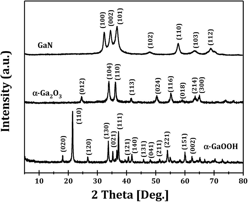 | ||
| Fig. 1 XRD patterns of GaOOH, Ga2O3 and GaN prepared at R = 1. | ||
Fig. 2 shows the XRD patterns of Ga2O3 samples synthesized via forced hydrolysis at different R values and followed by calcination. All the samples exhibit similar diffraction peaks of α-Ga2O3 (JCPDS no. 06-0503), a monoclinic system and C2/m space group with a = b = 4.98 Å and c = 13.43 Å as its cell parameters.27 No diffraction peaks corresponding to impurity phases can be observed in all cases. We notice that, however, the intensities of diffraction peaks of Ga2O3 samples synthesized at different R values are different, indicating that different morphologies and/or crystallinities were obtained for these Ga2O3 samples. With increasing R value from 0.2 to 1, the relative crystallinity increases distinctly, while the relative crystallinity decreases with further increase in R value. That is, Ga2O3 with highest crystallinity can be obtained with optimized ionic strength ratio of 1 during forced hydrolysis.
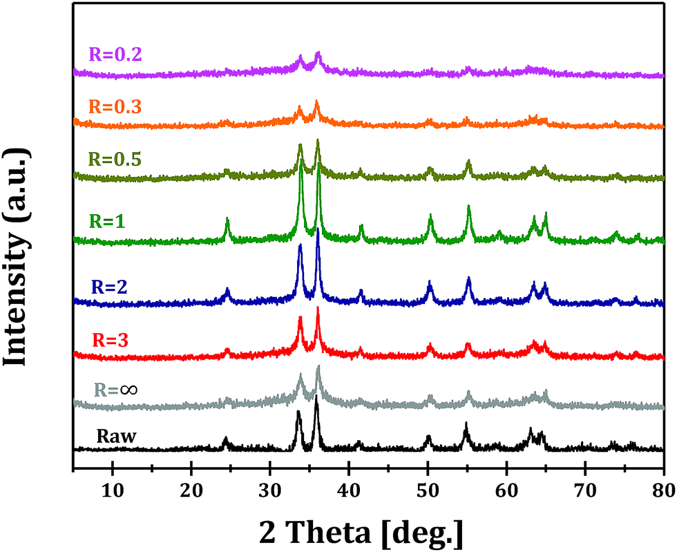 | ||
| Fig. 2 XRD patterns of Ga2O3 synthesized at different R values and Raw Ga2O3. | ||
Raman spectroscopy is further employed to determine the structure of as-prepared Ga2O3 samples. As shown in Fig. S1,† Raman bands at 410, 560 and 700–710 cm−1 are observed in the 300–1000 cm−1 region, corresponding to the Eg, A1g and Eg modes of α-Ga2O3, respectively.1,28 The Raman bands broadening and the noticeable shifts of bands at 700–710 cm−1 are due to the presence of surface defects on the samples.
The XRD patterns of GaN samples from the nitridation of different Ga2O3 samples are shown in Fig. 3. Pure GaN phase of wurtzite structure and P63mc space group with a = b = 3.189 Å and c = 5.185 Å as its cell parameters is obtained in all cases.27 We also notice the different intensities of diffraction peaks, similar to the trend observed for Ga2O3 samples. It can be proposed that the morphologies and crystallinities of Ga2O3 samples are preserved, at least partially preserved, through nitridation at elevated temperature of 950 °C. Raman spectra of GaN samples are presented in Fig. S2† and a series of Raman bands can be observed in the 300–1000 cm−1 region. The band at 420 cm−1 is related to the N-rich structure of GaN,29 while the shifts of other Raman bands, e.g. at 515, 595 and 695 cm−1, compared with standard hexagonal GaN, should be related to the formation of abundant defects on the surface.20
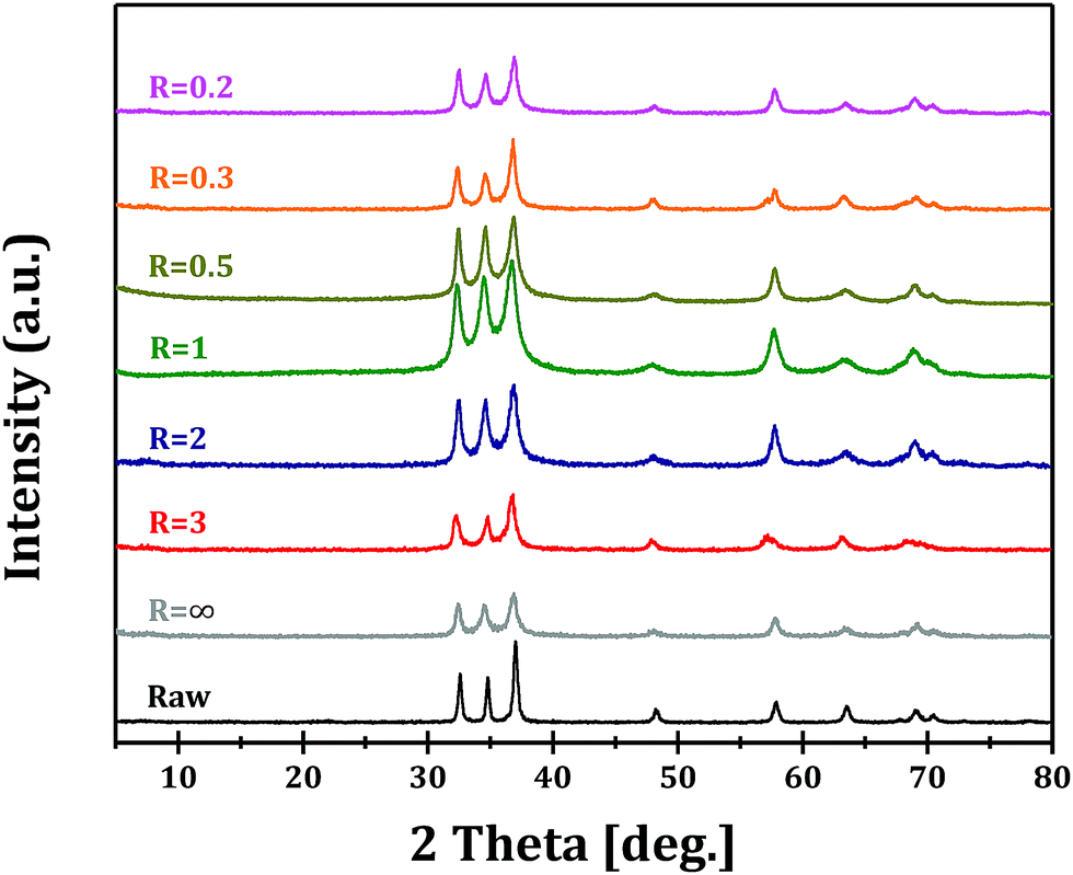 | ||
| Fig. 3 XRD patterns of GaN from the nitridation of Ga2O3 synthesized at different R values and Raw Ga2O3. | ||
The SEM images of Ga2O3 samples synthesized by forced hydrolysis at different R values are shown in Fig. 4. It is very clear that different morphologies are obtained at different ratios of ionic strength during forced hydrolysis, i.e. R values. At R = ∞, Ga2O3 crystals appear as spindle-like nanorods with two narrow sides and a wide center (Fig. 4a). At R = 3 and 2, Ga2O3 crystals appear as nanorods with the same broad sides and center (Fig. 4b and c). With decreasing R value to 1, Ga2O3 crystals transform to dumbbell-shaped nanorods with two wide sides and narrow center (Fig. 4d). Further decrease in the ratio of ionic strength during forced hydrolysis (R = 0.5 and 0.3) results in the exfoliation of nanorods to nanoplates and strips and fragments (Fig. 4e and f). At R = 0.2, the Ga2O3 crystals are totally broken up to fragments. According to the SEM images of Ga2O3 samples synthesized at different R values, we can infer that the crystallinities of Ga2O3 samples vary with R values. The highest crystallinity of Ga2O3 sample is obtained at the R value of 1, in accordance with the results from XRD patterns (Fig. 2). The surface areas of Ga2O3 samples synthesized at different R values are measured to be in the range of 30–50 m2 g−1, distinctly higher than commercial Ga2O3 (15 m2 g−1).
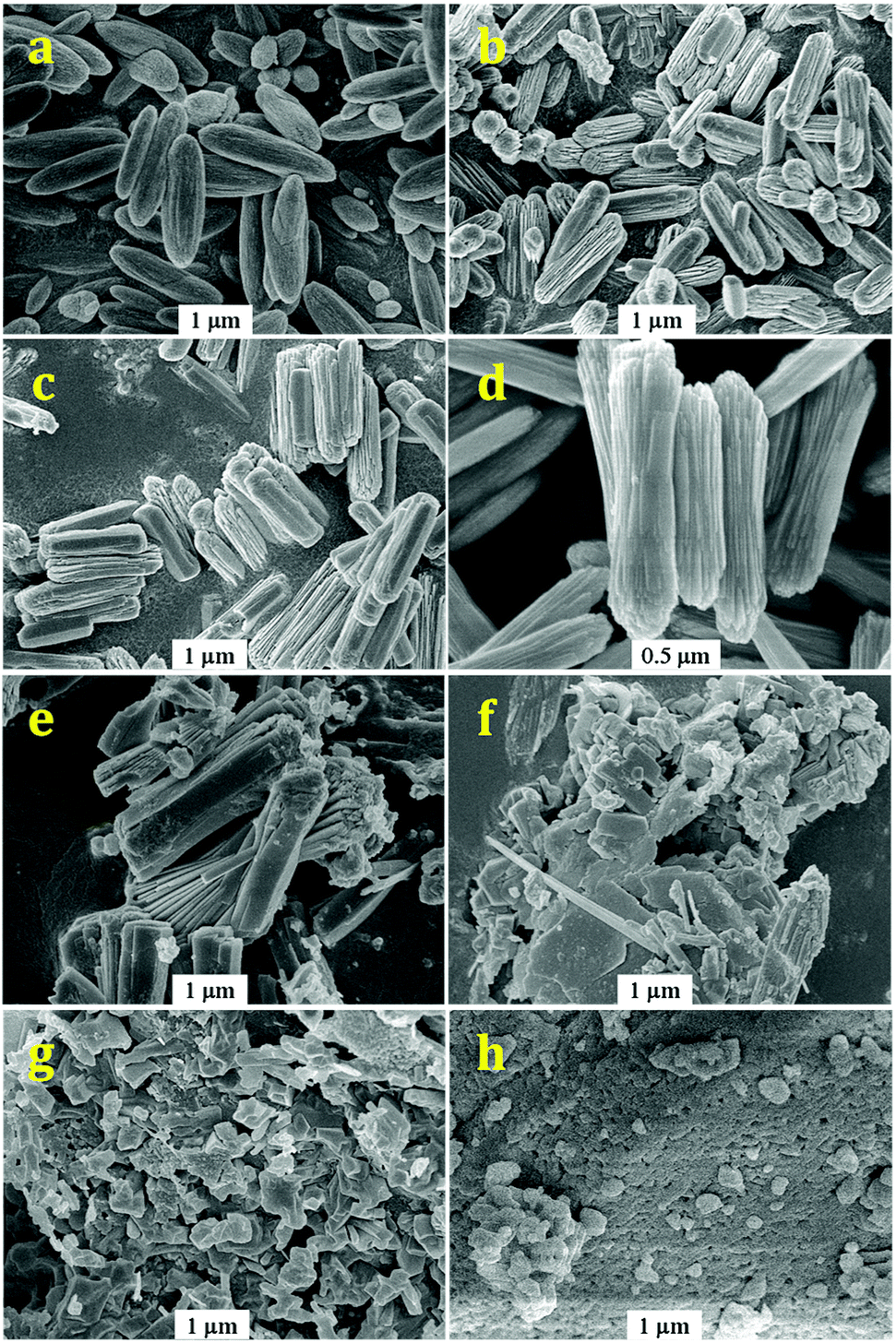 | ||
| Fig. 4 SEM images of Ga2O3 synthesized at different R values: R = ∞ (a); R = 3 (b); R = 2 (c); R = 1 (d); R = 0.5 (e); R = 0.3 (f); R = 0.2 (g) and Raw Ga2O3 (h). | ||
Fig. 5 shows the SEM images of GaN samples obtained from the nitridation of Ga2O3 samples. It is seen that the overall shape of GaN sample follows its Ga2O3 precursor. However, after careful observation, we find that some tiny nanoparticles do exist on the external surface of GaN crystals. These observations indicate that nitridation starts from a local point of Ga2O3 crystal. The surface areas of as-obtained GaN samples are measured to be 40–60 m2 g−1, even higher than parent Ga2O3 (30–50 m2 g−1) due to the formation of tiny nanoparticles on the surface. To confirm the phase purity of as-obtained GaN samples, the energy-dispersive X-ray mapping analysis was performed on representative GaN sample (R = 1). As shown in Fig. S3,† the homogeneous distribution of Ga and N species in selected GaN crystal grain is clearly observed (Ga/N = 0.86; Ga/N < 1 due to the presence of N-containing impurities), ruling out the formation of metallic Ga islands from nitridation at high temperature of 950 °C.
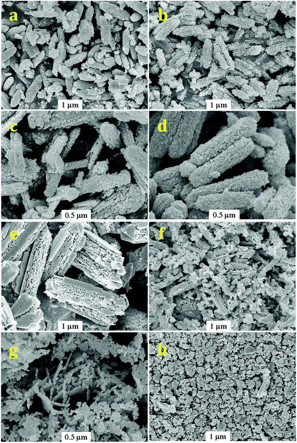 | ||
| Fig. 5 SEM images of GaN from the nitridation of Ga2O3 synthesized at different R values: R = ∞ (a); R = 3 (b); R = 2 (c); R = 1 (d); R = 0.5 (e); R = 0.3 (f); R = 0.2 (g) and Raw Ga2O3 (h). | ||
For a more clear view of the morphology changes during nitridation, TEM images of Ga2O3 and GaN samples synthesized at R = 1 are shown in Fig. 6. A typical Ga2O3 crystal assembly appears as a nanorod with length of 2 μm and diameter of 0.4 μm (Fig. 6a). In the HRTEM images (Fig. 6b and c), clear lattice fringes with interplanar spacing of 0.249 nm are observed, corresponding to the (110) planes of Ga2O3 crystal. After nitridation, the overall shape of Ga2O3 is well preserved (Fig. 6d), in accordance with SEM observations. It is also found that the GaN crystal assembly is composed of tiny nanoparticles with sizes of a few to a dozen nanometers. Accordingly, some nanoscale mesopores can be observed in GaN crystal assembly. HRTEM images (Fig. 6e and f) reveal the lattice fringes with interplanar spacing of 0.276 nm, corresponding to the (100) planes of GaN crystal.
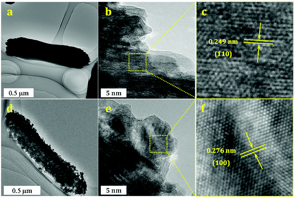 | ||
| Fig. 6 TEM images (a, d), HRTEM images (b, e) and enlarged view of HRTEM images (c, f) of Ga2O3 and GaN samples synthesized at R = 1. | ||
On the basis of SEM (Fig. 4) and TEM observations (Fig. 6), we demonstrate that Ga2O3 samples with different morphologies can be prepared via controlling the ratio of ironic strength during forced hydrolysis. With decreasing R value, the morphology of Ga2O3 crystals gradually transforms from spindle-like to dumbbell-shaped nanorods and then to exfoliated fragments, which gives us a hint on the formation process of Ga2O3 sample.
A schematic diagram of morphology-controlled synthesis of Ga2O3 via forced hydrolysis route is summarized in Fig. 7. In the first step, different ratios of Ga(NO3)3·nH2O, NaNO3 and urea are mixed in deionized water and heated at 90 °C to form unstable Ga(OH)3 transition state. Then, the unstable Ga(OH)3 transition state crystallizes to different morphologies of α-GaOOH at 90 °C with the presence of different concentrations of sodium ions as structure-directing and mineralizing agents. In the final step, GaOOH is transformed to α-Ga2O3 through calcination in vacuum, with its morphology well preserved. Besides, the as-obtained α-Ga2O3 can be transformed to GaN with overall morphology well preserved (Fig. 6).
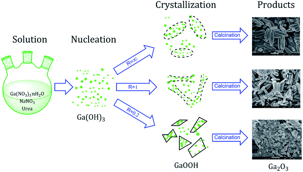 | ||
| Fig. 7 Schematic diagram of morphology-controlled synthesis of Ga2O3 via forced hydrolysis route. | ||
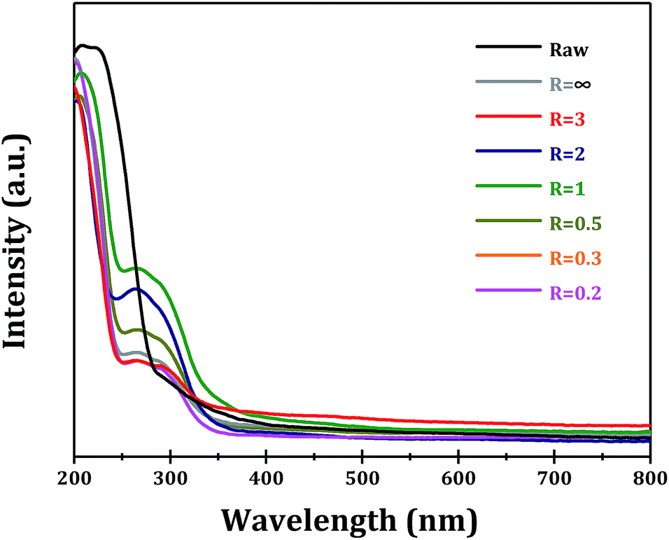
The optical properties of as-obtained α-Ga2O3 samples with different morphologies are examined to explore the possible morphology-dependent effects. The UV-vis spectra of α-Ga2O3 synthesized at different R values are shown in Fig. 8. Commercial α-Ga2O3 sample (Raw) shows significant absorption in the ultraviolet region with edge up to ∼290 nm, corresponding to the band gap of ∼4.3 eV. While for α-Ga2O3 samples prepared via forced hydrolysis, two absorption peaks can be distinguished, i.e. intrinsic absorption with edge up to ∼260 nm (4.8 eV) and sub-band absorption with edge up to ∼360 nm (3.5 eV). The sub-band absorption should be related with the existence of abundant defect sites in α-Ga2O3, e.g. oxygen vacancies as proposed in other oxide semiconductors.30,31 It is seen that the highest absorption with edge up to ∼360 nm is obtained with α-Ga2O3 sample at R = 1, indicating its highest defect site concentration.
 | ||
| Fig. 8 UV-vis spectra of Ga2O3 synthesized at different R values. | ||
For GaN samples from the nitridation of α-Ga2O3 samples, significant absorption in the ultraviolet and visible region is observed (Fig. S4†). The band-edge energy cannot be distinguished due to the overlap by sub-band absorption as well as the serious light scattering effects caused by the formation of mesoporous structure (Fig. 5 and 6).
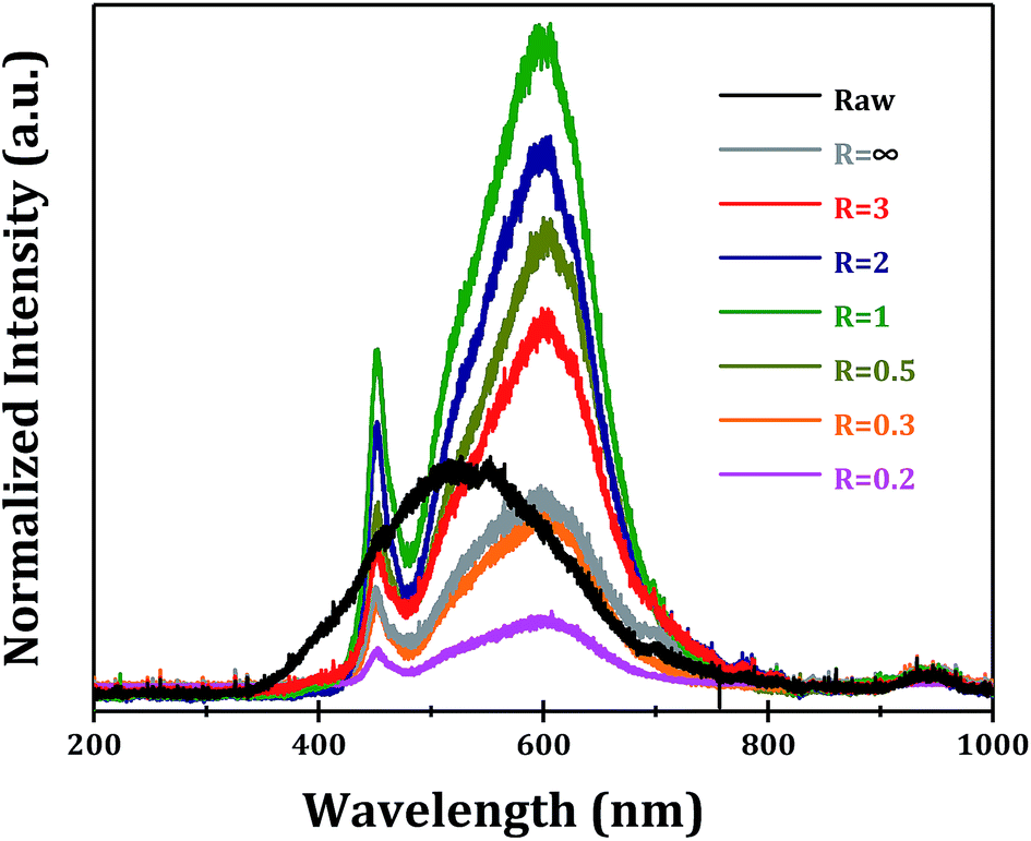
The photoluminescence properties of α-Ga2O3 samples synthesized at different R values are examined. It is known that the photoluminescence emissions are originated from the radiative recombination of photo-generated electrons and holes on semiconductors. Two major photo-physical processes, i.e. direct band–band transition and indirect transition from trapping states, can give rise to photoluminescence signals. Under 270 nm ultraviolet light excitation, a broad photoluminescence signal from 350 to 700 nm (centered at 500 nm) is observed for commercial α-Ga2O3 sample (Fig. 9). While for α-Ga2O3 samples prepared via forced hydrolysis followed by calcination, two significant photoluminescence signals at 460 (blue photoluminescence) and 600 nm (orange photoluminescence) are observed. The blue photoluminescence signal should be originated from the recombination of photogenerated electrons on donors and holes on acceptors while the orange photoluminescence from the recombination on deep trapping states.32,33 Undoubtedly, all these two photoluminescence signals are associated with the defect sites in as-prepared α-Ga2O3 samples, which distinguish them from commercial sample. In this context, the intensity of photoluminescence signals is determined by both the defect sites and the crystallinity of the sample. We find that the sequence of photoluminescence intensity (Fig. 9) correlates well with the optical absorption (Fig. 8), both of which indicate the morphology-dependent optical properties of α-Ga2O3 samples. At R = 1, the highest photoluminescence intensity is obtained, several times higher than commercial α-Ga2O3 sample.
 | ||
| Fig. 9 Photoluminescence spectra of Ga2O3 synthesized at different R values. | ||
We also investigate the optical properties of GaN samples prepared from the nitridation of α-Ga2O3 samples and the results are shown in Fig. S5.† Significant photoluminescence signals at 380 and 450 nm are observed for all samples in the 350–480 nm region, and the highest photoluminescence intensity is obtained with GaN (R = 1). Besides, we cannot draw other convincing conclusions on the morphology-dependent effects due to the serious light scattering effects caused by the formation of mesoporous structure. Further researches on these issues are still in progress.
Conclusions
In summary, we have successfully developed a forced hydrolysis route to α-GaOOH starting from inorganic gallium salt and urea as raw materials, and we have realized the morphology control by adjusting the ratios of ionic strength in the synthesis system, i.e. Ga3+/Na+. The as-prepared α-GaOOH nanorods can be transformed to α-Ga2O3 nanorods upon simple calcination with the morphology well preserved, and be further transformed to GaN nanocrystal assembles through nitridation. This process provides a top-down strategy to Ga2O3 and GaN nanocrystals. Typically, the morphology of as-obtained α-Ga2O3 crystals gradually transform from spindle-like to dumbbell-shaped nanorods and then to exfoliated fragments with decreasing ratios of ionic strength in the synthesis system. While for the GaN samples prepared from nitridation at elevated temperature, the overall shape of α-Ga2O3 precursor can be preserved and nanoscale mesopores originated from nanoparticles assembling are clearly observed.The UV-vis absorption and photoluminescence properties of Ga2O3 crystals with different morphologies are examined, and the results clearly demonstrate the morphology-dependent effects. The methodology presented here may be extended to the synthesis and applications of other oxide and nitride semiconductors.
Conflicts of interest
There are no conflicts to declare.Acknowledgements
This work is financially supported by the National High Technology Research and Development Program of China (2015AA033303) the National Natural Science Fund of China (21421001).Notes and references
- X. Wang, Q. Xu, M. Li, S. Shen, X. Wang, Y. Wang, Z. Feng, J. Shi, H. Han and C. Li, Angew. Chem., Int. Ed., 2012, 51, 13089–13092 CrossRef CAS PubMed.
- K. Maeda, T. Takata, M. Hara, N. Saito, Y. Inoue, H. Kobayashi and K. Domen, J. Am. Chem. Soc., 2005, 127, 8286–8287 CrossRef CAS PubMed.
- T. Ohno, L. Bai, T. Hisatomi, K. Maeda and K. Domen, J. Am. Chem. Soc., 2012, 134, 8254–8259 CrossRef CAS PubMed.
- P. Parkinson, C. Dodson, J. J. Joyce, K. A. Bertness, N. A. Sanford, L. M. Herz and M. B. Johnston, Nano Lett., 2012, 12, 4600–4604 CrossRef CAS PubMed.
- T. Hashimoto, F. Wu, J. S. Speck and S. Nakamura, Nat. Mater., 2007, 6, 568–571 CrossRef CAS PubMed.
- J. Hejtmánek, K. Knížek, M. Maryško, Z. Jirák, D. Sedmidubský, Z. Sofer, V. Peřina, H. Hardtdegen and C. Buchal, J. Appl. Phys., 2008, 103, 07D107 CrossRef.
- Z. Sofer, D. Sedmidubský, J. Stejskal, J. Hejtmánek, M. Maryško, K. Jurek, M. Václavů, V. Havránek and A. Macková, J. Cryst. Growth, 2008, 310, 5025–5031 CrossRef CAS.
- X. F. Wang, J. H. Tong, X. Chen, B. J. Zhao, Z. W. Ren, D. W. Li, X. J. Zhuo, J. Zhang, H. X. Yi, C. Liu, F. Fang and S. T. Li, Chem. Commun., 2014, 50, 682–684 RSC.
- C. T. Huang, J. H. Song, W. F. Lee, Y. Ding, Z. Y. Gao, Y. Hao, L. J. Chen and Z. L. Wang, J. Am. Chem. Soc., 2010, 132, 4766–4771 CrossRef CAS PubMed.
- R. Zou, Z. Zhang, Q. Liu, J. Hu, L. Sang, M. Liao and W. Zhang, Small, 2014, 10, 1848–1856 CrossRef CAS PubMed.
- W. Han, S. Fan, Q. Li and Y. Hu, Science, 1997, 277, 1287–1289 CrossRef CAS.
- X. Sun and Y. Li, Angew. Chem., Int. Ed., 2004, 43, 3827–3831 CrossRef CAS PubMed.
- J. Wallys, J. Teubert, F. Furtmayr, D. M. Hofmann and M. Eickhoff, Nano Lett., 2012, 12, 6180–6186 CrossRef CAS PubMed.
- J. C. Johnson, H. J. Choi, K. P. Knutsen, R. D. Schaller, P. D. Yang and R. J. Saykally, Nat. Mater., 2002, 1, 106–110 CrossRef CAS PubMed.
- Y. J. Hwang, C. H. Wu, C. Hahn, H. E. Jeong and P. D. Yang, Nano Lett., 2012, 12, 1678–1682 CrossRef CAS PubMed.
- P. Huang, H. Zong, J. J. Shi, M. Zhang, X. H. Jiang, H. X. Zhong, Y. M. Ding, Y. P. He, J. Lu and X. D. Hu, ACS Nano, 2015, 9, 9276–9283 CrossRef CAS PubMed.
- J. Goldberger, R. R. He, Y. F. Zhang, S. W. Lee, H. Q. Yan, H. J. Choi and P. D. Yang, Nature, 2003, 422, 599–602 CrossRef CAS PubMed.
- C. L. Chen, M. M. C. Chou, T. Yan, H. C. Huang, C. Y. J. Lu and C. H. Chen, Chem. Commun., 2014, 50, 5695–5698 RSC.
- Z. Sofer, D. Sedmidubský, Š. Huber, J. Hejtmánek, A. Macková and R. Fiala, Int. J. Nanotechnol., 2012, 9, 809–824 CrossRef CAS.
- Z. Sofer, D. Sedmidubský, Š. Huber, P. Šimek, F. Šaněk, O. Jankovský, E. Gregorová, R. Fiala, S. Matěějková and M. Mikulics, J. Nanopart. Res., 2013, 15, 1411 CrossRef.
- P. Šimek, D. Sedmidubský, Š. Huber, K. Klímová, M. Maryško, M. Mikulics and Z. Sofer, Mater. Chem. Phys., 2015, 164, 108–114 CrossRef.
- X. Chen, J. Xu, R. M. Wang and D. Yu, Adv. Mater., 2003, 15, 419–421 CrossRef CAS.
- Y. Xie, Y. Qian, W. Wang, S. Zhang and Y. Zhang, Science, 1996, 272, 1926–1927 CrossRef CAS PubMed.
- X. Liu, G. Qiu, Y. Zhao, N. Zhang and R. Yi, J. Alloys Compd., 2007, 439, 275–278 CrossRef CAS.
- T. Ogi, Y. Kaihatsu, F. Iskandar, E. Tanabe and K. Okuyama, Adv. Powder Technol., 2009, 20, 29–34 CrossRef CAS.
- W. H. R. Shaw and J. J. Bordeaux, J. Am. Chem. Soc., 1955, 77, 4729–4733 CrossRef CAS.
- M. Muruganandham, R. Amutha, M. S. M. A. Wahed, B. Ahmmad, Y. Kuroda, R. P. S. Suri, J. J. Wu and M. E. T. Sillanpää, J. Phys. Chem. C, 2012, 116, 44–53 CAS.
- D. Machon, P. F. McMillan, B. Xu and J. Dong, Phys. Rev. B, 2006, 73, 094125 CrossRef.
- J. Q. Ning, S. J. Xu, D. P. Yu, Y. Y. Shan and S. T. Le, Appl. Phys. Lett., 2007, 91, 103117 CrossRef.
- J. Yan, T. Wang, G. Wu, W. Dai, N. Guan, L. Li and J. Gong, Adv. Mater., 2015, 27, 1580–1586 CrossRef CAS PubMed.
- L. Li, J. Yan, T. Wang, Z. J. Zhao, J. Zhang, J. Gong and N. Guan, Nat. Commun., 2015, 6, 5881 CrossRef PubMed.
- T. Harwig and F. Kellendonk, J. Solid State Chem., 1978, 24, 255–263 CrossRef CAS.
- L. Binet and D. Gourier, J. Phys. Chem. Solids, 1998, 59, 1241–1249 CrossRef CAS.
Footnote |
| † Electronic supplementary information (ESI) available. See DOI: 10.1039/c7ra10639d |
| This journal is © The Royal Society of Chemistry 2017 |