
 Open Access Article
 This Open Access Article is licensed under a
 Creative Commons Attribution 3.0 Unported Licence
Self-powered UV-visible photodetector with fast response and high photosensitivity employing an Fe:TiO2/n-Si heterojunction†
Lin Suna,
Chunrui Wang *a,
Tao Jiab,
Jiale Wanga,
Gyu-Chul Yic and
Xiaoshuang Chenad
*a,
Tao Jiab,
Jiale Wanga,
Gyu-Chul Yic and
Xiaoshuang Chenad
aDepartment of Applied Physics, State Key Laboratory for Modification of Chemical Fibers and Polymer Materials, Donghua University, 2999 Renmin Rd North, Songjiang District, Shanghai, P. R. China. E-mail: crwang@dhu.edu.cn
bSchool of Fundamental Studies, Shanghai University of Engineering Science, 333 Long Teng Road, Songjiang District, Shanghai, P. R. China
cDepartment of Physics and Astronomy, Seoul National University, Seoul 151-747, Korea. E-mail: gcyi@snu.ac.kr
dNational Laboratory for Infrared Physics, Shanghai Institute of Technical Physics, Chinese Academy of Science, Shanghai 200083, P. R. China. E-mail: xschen@mail.istp.ac.cn
First published on 8th November 2017
Abstract
An ultrasensitive, fast response and self-powered photodetector would be preferable in practical applications. In this paper, we report fast response, high photosensitivity and self-powered Fe doped TiO2 (Fe:TiO2)/n-Si UV-visible detectors via a facile solution process. As-fabricated devices exhibited excellent photoresponse properties, including high responsivity of 46 mA W−1 (350 nm) and 60 mA W−1 (600 nm) with 0.5 mW cm−2 light irradiation under zero bias, as well as an ultrasensitive (on/off ratio up to 103), fast (rise/decay time of <10/15 ms), and broad-band (UV-visible) photodetection with no or low external energy supply. Furthermore, the quantum efficiency of the heterojunction rose up beyond 100% with a broad wavelength range at a small reverse bias of −0.5 V. The self-power originated from the existence of a built-in electric field between Fe:TiO2 and Si that helps facilitate the separation of photogenerated electron–hole pairs and regulate the electron transport. Capacitance–voltage (C–V) measurements of Fe:TiO2/n-Si devices also confirmed the existence of the built-in electric field. Such Fe:TiO2/n-Si heterojunction photodetectors might be potentially useful for relative applications with weak-signal fast detection in the UV-visible band.
Introduction
In recent years, functional nanosystems must not only be sensitive, controllable and multifunctional, but must also have a low power consumption. Self-driven or self-sufficient nanodevices and nanosystems have recently attracted a lot of attention due to their various superior performance advantages.1,2 Among them, many reports about self-powered photodetectors (PDs) have proved that they can operate independently and sustainably.3–11 This not only enhances the adaptability of the device, but also greatly reduces the size and cost of the system. In practical applications including imaging techniques, light-wave communication, and environmental sensing, ultrasensitive and fast response self-powered PDs would be more urgently needed. However, small photocurrent response, slow temporal recovery, narrow range of detectable light wavelengths and high detectable light intensities are the limitations for self-powered PDs. In addition, photoelectrochemical (PEC) self-powered systems have the problems of electrolyte toxicity and volatilization, and most of the PEC PDs only respond to the ultraviolet band region.5,6 Some routes introducing plasmonic materials,7 ferroelectric materials,8 monolayer graphene film as transparent electrode,9 high-quality single crystals obtained via molecular beam epitaxy10 have been developed to further improve device performance. However, additional complexity of the processing and the high cost limit their practical applications. Therefore, high performance and reliable self-powered PDs fabricated by a facile and low cost way is necessary.Benefiting from the mature silicon (Si)-based process in the microelectronics industry, semiconductor/Si vertical heterojunction PDs, with a planar device structure, have attractive applications in the optoelectronic integrated circuits.12–17 The construction of semiconductor nanostructure materials/Si heterojunction can not only compensate for the limited spectral bandwidth of Si due to the extensive absorption spectra of different semiconductor materials (especially for UV applications), but also promote the separation and transport of photo-induced carriers. Among them, wide-bandgap semiconductor materials ZnO and TiO2 has been widely investigated. In contrast, the chemical stability of TiO2 is more stable than ZnO. And it has been proved that the optical sensitivity and activity of TiO2 can be improved by ion doping. Ion doping of TiO2 either introduce impurity energy level(s) or adding energy states to band edge, as a consequence, spectral response range can be broadened.18–23 In Fe-doped TiO2 (Fe:TiO2), Fe3+ ions tend to substitute for Ti4+ ions and take their lattice sites. Fe3+ cations can act as shallow traps to decrease of the recombination rate (see Fig. S4, ESI†).17 Some good self-powered PDs based on TiO2 have been reported, such as TiO2–SnO2,6 TiO2–PANI,24 TiO2–CH3NH3PbI3 (ref. 25) and so on. But as far as we know, there are few reports on photodetection with doping of TiO2. Herein, we designed a novel self-powered UV-visible PD employing heterojunction between the Fe:TiO2 and Si. Such Fe:TiO2/n-Si heterojunction fabricated by a facile and low cost way, with high performance and reliable PDs, it can be used for broad-band (UV-visible) photodetection in a self-powered mode operation. The built-in electric field formed between the interfaces creates the driving force for the fast and efficient separation of the photogenerated carriers. A fast response speed of 10/15 ms were achieved in the fabricated PDs. Notably, under zero bias, the device exhibited high responsivity of 46 mA W−1 (350 nm) and 60 mA W−1 (600 nm) with a 0.5 mW cm−2 light irradiation. At a small reverse bias of −0.5 V, the quantum efficiency of the device rose up beyond 100% with a UV-visible wavelength range. The novel device design described in this paper may point out a promising new direction for manufacturing advanced self-powered PDs.
Experimental
Materials synthesis and characterization
3 mL of tetrabutyl titanate (C16H36O4Ti) solution was stirred with 10 mL of ethanol solution overnight, and 0.02 M anhydrous ferric chloride (FeCl3) ethanol solution was stirred overnight. Two sols were mixed with magnetic stirring until homogeneous. The above process avoided water involvement. Light yellow sol was spin-coated at n-Si (111) (8–13 Ω cm) wafer with 1000 rpm for 10 s. Subsequently annealed under an air atmosphere in muffle furnace at 400 °C for 1 hour and spontaneously cooled to room temperature. Namely, Fe:TiO2/n-Si heterojunction nanostructure samples were obtained.Morphology of Si/TiO2 heterojunction were determined by a field emission scanning electron microscope (FESEM, Hitachi, S-4800). Powder X-ray diffraction (XRD) of the samples was conducted by a D/max-2550VB+/PC X-ray diffractometer (Rigaku, Japan) equipped with a rotating anode and a Cu Kα radiation source (λ = 1.54056 Å). Raman spectra were recorded at room temperature on an inVia-Reflex micro-Raman spectroscopy system from Renishaw with 532 nm radiation. Room temperature UV-vis absorption spectroscopy was conducted on a Shimadzu UV3600 UV-vis-NIR spectrophotometer. XPS data were obtained using an Escalab 250Xi (Thermo Scientific) spectrometer with an excitation source of Al-Kα radiation. Photoluminescence (PL) measurements were carried out at room temperature using fluorescence spectroscopy (PTI QuantaMaster) with a xenon lamp as the excitation source (λex = 370 nm).
Photodetector fabrication and measurement
The top electrode is Ag-planted digitated finger shape with total surface area of 25 mm2. The bottom of the Si wafer was coated with an Ag layer as a bottom electrode. To illustrate the reliability of the manufacturing process, sample A, B, C and D were prepared under the same conditions, and the following test data was based on sample A if there are no special instructions. The current–voltage (I–V) curves and capacitance–voltage (C–V) characteristic of the device were measured by using the Keithley-4200 semiconductor characterization system (SCS) on a probe station at room temperature. Monochromatic light with wavelength ranging from 350 to 600 nm was achieved from a 300 W Xenon lamp with monochromators.Results and discussion
Characterization
SEM image showing the morphology and structure of as-fabricated heterojunctions consisting of TiO2 and Fe:TiO2 thin film/Si wafer via a solution process of spin coating (Fig. 1a and b). As can be seen from the cross-section of heterojunction, the nanoscale particles formed a dense film with a thickness of about 200 nm. The pure and Fe-doped TiO2 were characterized by XRD. As shown in Fig. 1c, all XRD peaks are indexed to the TiO2 anatase phase (JCPDS card no. 21-1272). No feature of Fe2O3 was detected for Fe-doped sample and all peaks were similar for both doped and undoped samples. It indicated that the TiO2 crystalline structure did not noticeably influenced by low-doping Fe. Raman spectra was used to further investigate the structural changes of TiO2 after doping. All peaks from Raman spectra can be assigned to Eg (147 cm−1, 199 cm−1 and 639 cm−1), B1g (398 cm−1) and A1g + B2g (517 cm−1) mode of anatase TiO2, which almost have not change in comparison with that of undoped TiO2 due to the low-dose implant for TiO2 (Fig. 1b). XPS analysis was used to investigate the change of surface chemical bonds of the TiO2 nanoparticles induced by iron as shown in Fig. 1e–g. Fig. 1e shows the O 1s core level spectra of Fe:TiO2. The peaks at 531.67 and 530.07 eV can be attributed to Si–O and Ti–O bonds. Ti 2p1/2 and Ti 2p3/2 spin-orbital splitting photoelectrons for Fe:TiO2 sample are located at binding energies of 464.47 and 458.77 eV (Fig. 1f), respectively, which are in agreement with the values of Ti4+ in TiO2. For the low doping level, the signals of Fe are weak (Fig. 1g). The binding energy at 711.27 eV and 724.47 eV should be assigned to 2p3/2 and 2p1/2 of Fe3+, respectively. These data exhibited a positive shift compared to those in Fe2O3 (2p3/2 and 2p1/2 of Fe3+ at 710.7 eV and 724.3 eV, respectively),26 probably indicative of more positively charged surface Fe3+. The slight enhancement of Fe 2p level binding energy can be attributed to the diffusion of Fe3+ into TiO2 lattice and the formation of Fe–O–Ti bond in the samples.27–30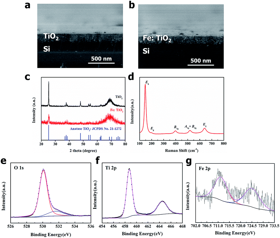 | ||
| Fig. 1 Characterizations of the Fe:TiO2/Si heterostructure. Cross-sectional SEM image of the (a) TiO2/Si and (b) Fe:TiO2/Si heterostructure. (c) XRD patterns of pure TiO2 film and Fe-doped TiO2 film. (d) Typical Raman spectrum of the Fe:TiO2 films. (e, f and g) The core-level spectra of (e) O 1s, (f) Ti 2f and (g) Fe 2p in the Fe:TiO2 films. | ||
Photoresponse of Fe:TiO2/n-Si heterojunction photodetector
We measured the light intensity dependence of the Fe:TiO2/n-Si heterojunction PD. Fig. 2a shows the current–voltage (I–V) curves of the Fe:TiO2/n-Si heterojunction device under 365 nm light with increasing incident light powers from 0.2 to 1.4 mW cm−2. The I–V curves of the photodetector exhibited a good rectifying behavior. When the light illuminates on the device, the negative biased current increased with increasing the incident light power. With the reverse voltage increasing, the Iph (photocurrent) rose sharply and subsequently reached saturation rapidly. The increasing electric field can separate electron–hole pairs sufficiently and promptly, giving rise to the increase of the photocurrent. But when the bias is sufficiently large, owing to the available number of charge carriers excited by the fixed illumination power, the photocurrent saturates.28 Another interesting finding is that the forward current keeps almost constant regardless of the power density. While in the forward bias, the barrier height and width enlarged, and electrons and holes could not tunnel from it, leading to no variation of forward current.27 Fig. 2b presents the dependence of photocurrent on the power density at different reverse biases. For lower reverse bias, the photocurrent increased nonlinearly with increasing the power density, while for higher reverse bias, the photocurrent was linearly related to the power density (see Fig. 2b). In general, the dependence of photocurrent on light intensity satisfies the relationship Iph ∝ Pθ, where P is the light intensity and θ is an empirical value related to the recombination processes of the photoexcited carriers.33 By fitting the curves in Fig. 2b, we obtained θ = 0.97 at reverse bias of −1 V, indicating that low trap states in Fe:TiO2/n-Si heterojunction photodetectors.14,33,34 Fig. 2c shows the photovoltage responsivity as a function of the incident light power. The absolute device responsivity RV (= VOC/P, VOC is the open-circuit voltage) exceeded 102 V W−1 at incident light powers from 0.2 to 1.4 mW cm−2. It can be as another important parameter for weak signal detection.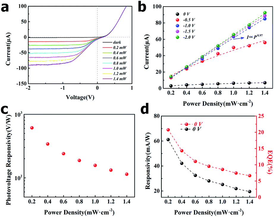 | ||
| Fig. 2 Photoresponse of Fe:TiO2/Si heterojunction with the device area = 0.25 cm2. (a) I–V characteristics of the heterojunction photodetector under various incident light power. (b) Zero-biased photocurrent under different incident intensity. (c) The photovoltage responsivity as a function of incident light power. (d) Responsivity and EQE under different incident light power at zero bias. With the decrease of light intensity, the EQE increased to 20.8% at 0.2 mW cm−2. | ||
Responsivity (R) and external quantum efficiency (EQE) are important quality factors for photodetectors, which can be given by the following formulas:
 | (1) |
 | (2) |
To further investigate the wavelength-dependent characteristics of Fe:TiO2/n-Si heterojunction, I–V curves were recorded when the wavelength of the incident radiation was switched from 350 to 600 nm at a constant intensity of 0.5 mW cm−2 (Fig. 3). The photocurrent of Fe:TiO2/n-Si heterojunction was found to depend on the wavelength of the incident radiation. As shown in Fig. 3a, the photocurrent of the device increased quickly from −5.77 μA at 350 nm to −7.67 μA at the wavelength of 600 nm. The wavelength dependence of both photocurrent responsivity and EQE of the device are presented in Fig. 3b and c, respectively. Fig. 3d shows the photocurrent responsivity and EQE with different incident light wavelengths at zero bias. Notably, the EQE exceeded 10% when the wavelength of the incident radiation was switched from 350 to 600 nm at a constant intensity of 0.5 mW cm−2. Furthermore, EQE of the heterojunction rose up beyond 100% with a broad wavelength range at a small reverse bias of −0.5 V (Fig. 3c). Fig. S1† shows photoresponse characteristics of sample B, C and D. The results indicate that the as-fabricated Fe:TiO2/Si PDs have excellent reproducibility, suggesting a promising direction for manufacturing advanced self-powered PDs.
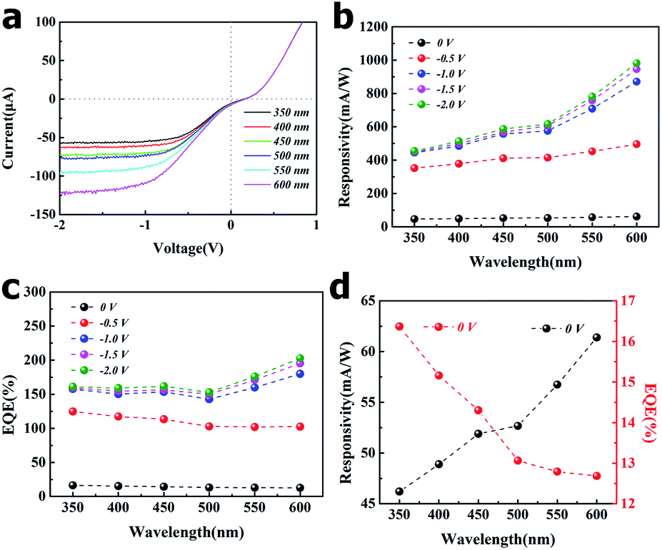 | ||
| Fig. 3 Photoresponse of Fe:TiO2/Si heterojunction with the device area = 0.25 cm2. When the wavelength of the incident radiation was switched from 350 to 600 nm at a constant intensity of 0.5 mW cm−2. (a) I–V characteristics of the heterojunction photodetector with various incident light wavelengths. The wavelength dependence of both (b) photocurrent responsivity and (c) EQE of the heterojunction under different biases. (d) Responsivity and EQE with different incident light wavelengths at zero bias. The EQE exceeded 10% when the wavelength of the incident radiation was switched from 350 to 600 nm. | ||
Fig. 4a is one cycle of the time-resolved photoresponse of the device at zero bias upon 365 nm light illumination at light intensity of 1.0 mW cm−2. Photoresponse time is defined as the time of switching duration from 10% to 90% of the pulse peak. From rising and falling edges, we can get rising time tr = 10 ms, falling time tf = 15 ms, respectively (detectable limit of our instrument). In Fig. 4b, the two on/off operational measurements interval one month maintained almost the same light response behaviors. Furthermore, our PDs showed strong response at zero bias voltage toward UV-visible light (0.5 mW cm−2, λ = 365, 400, 450, 500, 550 and 600 nm) as shown in Fig. 4c, suggesting a broadband detection spectrum. We collected photocurrent under different wavelengths with the same light power, and found that the linear correlation between photocurrent and the number of incident photons (see Fig. S2, ESI†). The bias-dependent switching characteristics of the photodetector were investigated by applying different bias voltages of 0, −0.5, −1.0, −1.5, and −2.0 V to the device is shown in Fig. 4d. As the bias voltage increases, the photocurrent increases significantly and eventually reaches a substantially constant. This result provides the possibility of adjusting the optical response of the device by applying an appropriate range of bias voltages.
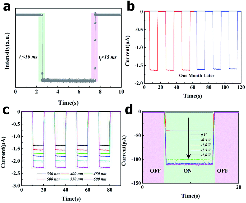 | ||
| Fig. 4 Time-dependent photocurrent response of the Fe:TiO2/Si device. (a) One cycle of photoswitching photocurrent at zero bias with a light of 365 nm. When the light is on, photocurrent increases sharply, and the rising photoresponse time is less than 10 ms. When the light is off, the photocurrent decreases to zero promptly, and the falling photoresponse time is less than 15 ms. (b) Stability measurement of device. The two on/off operational measurements interval one month maintained almost the same light response behaviors. (c) The photoresponse under various excitation wavelengths with the same light intensity of 0.5 mW cm−2. (d) Photocurrent switching behaviors obtained under different reverse bias voltages. | ||
Excellent photoresponse of the Fe:TiO2/Si heterojunction device can be explained by the processes of photo-excitation and carrier transport in the junction illustrated in energy band diagram (see Fig. 5). The Fe doped TiO2 layer could absorb UV light and part of short-wavelength visible light (see Fig. 5b and c). The photogenerated electron–hole pairs are only created inside TiO2 side under UV light and part of short-wavelength visible light, while the electron–hole pairs are only created inside Si side under visible light. TiO2 and Si form a space charge region as shown in Fig. 5b where part of the photo-generated electrons diffuse from TiO2 towards the junction and are swept into Si, while the photo-generated holes are confined in the Si side because of the large valence band offset. Since the presence of an internal electric field (at space charge region) facilitates the separation of electron–hole pairs under UV-visible light irradiation, which significantly reduces the electron–hole recombination ratio, resulting in much higher photocurrent. In the case of the reverse bias (positive bias is applied on Si sides shown in Fig. 5c), with the same direction of the internal electrical field, could promote the separation of the electron–hole pairs. Meanwhile, the width of the depletion layer narrows (the height of the barrier becomes low), and the generated electrons in the space charge region of TiO2 could transport through the depletion layer driven by the applied bias.35
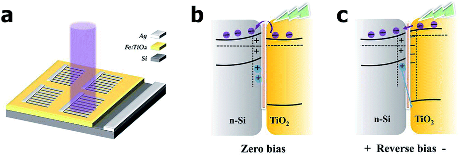 | ||
| Fig. 5 (a) Illustration of the schematic device. Schematic representation of the band energies and charge transfer of the Si(111)/TiO2 film under illumination with (b) zero bias and (c) reverse bias, respectively. | ||
High depletion region of heterostructure holds a powerful built-in electric field that rapidly separates photon-generating carriers, leading high quantum efficiency and fast response speed during thermal equilibrium. This make our PDs show self-powered properties with very fast temporal response, as well as excellent EQE and responsivity in UV-visible region. In addition, the vertical conductive distance between TiO2 film and the electrodes prevents unnecessary recombination, thereby further improving the response speed.31,32,36,37 In Fig. S3,† compared to TiO2 thin film PD in photoconductive mode, heterostructure PD has higher responsivity and faster response speed. Fig. S5† shows the PL spectra of pure TiO2 film and Fe-doped TiO2 film. The intensity increase of the PL from the Fe-doped TiO2, compared to pure TiO2, which indicated higher carrier concentration. Furthermore, a strong accelerating electric field is easily formed on thin film at the applied reverse bias, which could facilitate carrier separation and produce external gain.38 Moreover, the increased donor density of Fe-doped sample is expected to shift the Fermi level of TiO2 toward the conduction band. The upward shift of the Fermi level facilitates the charge separation at the interface by increasing the degree of band bending at the TiO2 surface. The enhanced charge separation and transportation are the major reasons for the observed better performance enhancement.
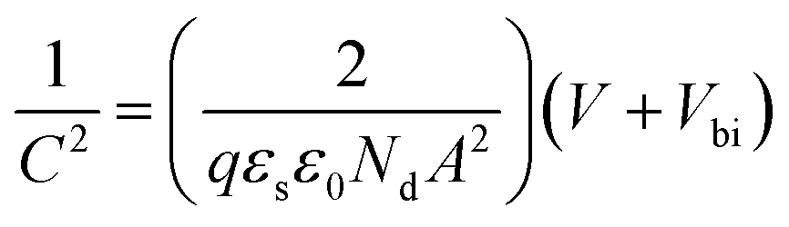
To verify the presence of built-in electric fields, the capacitance–voltage (C–V) measurements were conducted. As shown in Fig. 6, the C–V curves were performed at 10 kHz in dark condition (black curve line). Further analysis about the interface could be given by Mott–Schottky plot (red curve line). Based on the equation:39
 | (3) |
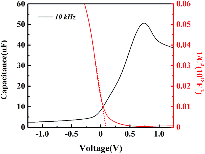 | ||
| Fig. 6 Capacitance–voltage measurement and Mott–Schottky plots of the Fe:TiO2/n-Si heterojunction at 10 kHz frequency. | ||
Conclusions
In summary, self-powered UV-visible PDs employing heterojunction between the Fe:TiO2 and Si was fabricated via a facile solution process. The existence of built-in electric field between Fe:TiO2 and Si help facilitate the separation of photo-generated electron–hole pairs and regulate the electron transport. A fast response speed of 10/15 ms were achieved. Under zero bias, the device exhibited high responsivity of 46 mA W−1 (350 nm) and 60 mA W−1 (600 nm) with a 0.5 mW cm−2 light irradiation. At a small reverse bias of −0.5 V, the EQE of the PD rose up beyond 100% with a broad wavelength range. The exploring of Fe:TiO2/n-Si heterojunction PD demonstrates an ultrasensitive, fast, and broad-band (UV-visible) photodetection with no or low external energy supply. We expect a productive future for the self-powered PDs integrated on flexible platforms, even multifunctional and smart systems.Conflicts of interest
There are no conflicts to declare.Acknowledgements
This work was supported by the National Natural Science Foundation of China under Grant No. 11174049 and 61376017, and the NSFC-NRF Scientific Cooperation Program, Brain Pool Program of Korea under grant: 171S-1-3-1829. J. W. would like to acknowledge Shanghai Talent Development Funding for financial support.References
- Z. L. Wang, Adv. Mater., 2012, 24, 280–285 CrossRef CAS PubMed.
- L. Peng, L. Hu and X. Fang, Adv. Funct. Mater., 2014, 24, 2591–2610 CrossRef CAS.
- L. Zheng, K. Hu, F. Teng and X. Fang, Small, 2017, 13, 1602448 CrossRef PubMed.
- Y. Q. Bie, Z. M. Liao, H. Z. Zhang, G. R. Li, Y. Ye, Y. B. Zhou, J. Xu, Z. X. Qin, L. Dai and D. P. Yu, Adv. Mater., 2011, 23, 649–653 CrossRef CAS PubMed.
- J. Y. Zhou, L. L. Chen, Y. Q. Wang, Y. M. He, X. J. Pan and E. Q. Xie, Nanoscale, 2016, 8, 50–73 RSC.
- X. Li, C. Gao, H. Duan, B. Lu, Y. Wang, L. Chen, Z. Zhang, X. Pan and E. Xie, Small, 2013, 9, 2005–2011 CrossRef CAS PubMed.
- A. A. Hussain, B. Sharma, T. Barman and A. R. Pal, ACS Appl. Mater. Interfaces, 2016, 8, 4258–4265 CAS.
- X. Wang, P. Wang, J. Wang, W. Hu, X. Zhou, N. Guo, H. Huang, S. Sun, H. Shen, T. Lin, M. Tang, L. Liao, A. Jiang, J. Sun, X. Meng, X. Chen, W. Lu and J. Chu, Adv. Mater., 2015, 27, 6575–6581 CrossRef CAS PubMed.
- B. Nie, J. G. Hu, L. B. Luo, C. Xie, L. H. Zeng, P. Lv, F. Z. Li, J. S. Jie, M. Feng, C. Y. Wu, Y. Q. Yu and S. H. Yu, Small, 2013, 9, 2872–2879 CrossRef CAS PubMed.
- D. Zheng, H. Fang, P. Wang, W. Luo, F. Gong, J. C. Ho, X. Chen, W. Lu, L. Liao, J. Wang and W. Hu, Adv. Funct. Mater., 2016, 26, 7690–7696 CrossRef CAS.
- Z. Zhang, Q. Liao, Y. Yu, X. Wang and Y. Zhang, Nano Energy, 2014, 9, 237–244 CrossRef CAS.
- I. S. Jeong, J. H. Kim and S. Im, Appl. Phys. Lett., 2003, 83, 2946–2948 CrossRef CAS.
- Y. Li, C. Y. Xu, J. Y. Wang and L. Zhen, Sci. Rep., 2014, 4, 7186 CrossRef CAS PubMed.
- H. Zhang, X. Zhang, C. Liu, S. T. Lee and J. Jie, ACS Nano, 2016, 10, 5113–5122 CrossRef CAS PubMed.
- A. Midya, A. Ghorai, S. Mukherjee, R. Maiti and S. K. Ray, J. Mater. Chem. A, 2016, 4, 4534–4543 CAS.
- Y. Wang, K. Ding, B. Sun, S.-T. Lee and J. Jie, Nano Res., 2016, 9, 72–93 CrossRef CAS.
- T. Ji, Q. Liu, R. Zou, Y. Sun, K. Xu, L. Sang, M. Liao, Y. Koide, L. Yu and J. Hu, Adv. Funct. Mater., 2016, 26, 1400–1410 CrossRef CAS.
- J. Guo, Z. Gan, Z. Lu, J. Liu, J. Xi, Y. Wan, L. Le, H. Liu, J. Shi and R. Xiong, J. Appl. Phys., 2013, 114, 104903 CrossRef.
- C.-C. Wang, K.-W. Wang and T.-P. Perng, Appl. Phys. Lett., 2010, 96, 143102 CrossRef.
- R. Asahi, T. Morikawa, T. Ohwaki, K. Aoki and Y. Taga, Science, 2001, 293, 269–271 CrossRef CAS PubMed.
- W. Li, Y. Wang, H. Lin, S. Ismat Shah, C. P. Huang, D. J. Doren, S. A. Rykov, J. G. Chen and M. A. Barteau, Appl. Phys. Lett., 2003, 83, 4143–4145 CrossRef CAS.
- I. S. Cho, C. H. Lee, Y. Feng, M. Logar, P. M. Rao, L. Cai, D. R. Kim, R. Sinclair and X. Zheng, Nat. Commun., 2013, 4, 1723 CrossRef PubMed.
- M. Anpo and M. Takeuchi, J. Catal., 2003, 216, 505–516 CrossRef CAS.
- L. Zheng, P. Yu, K. Hu, F. Teng, H. Chen and X. Fang, ACS Appl. Mater. Interfaces, 2016, 8, 33924–33932 CAS.
- H. Zhou, Z. Song, P. Tao, H. Lei, P. Gui, J. Mei, H. Wang and G. Fang, RSC Adv., 2016, 6, 6205–6208 RSC.
- C. D. Wagner, W. M. Riggs, L. E. Davis and J. F. Moulder, Handbook of X-Ray Photoelectron Spectroscopy, ed. G. E. Muilenberg, Perkin Elmer Corporation, Eden Prairie, 1979 Search PubMed.
- J. Zhu, F. Chen, J. Zhang, H. Chen and M. Anpo, J. Photochem. Photobiol., A, 2006, 180, 196–204 CrossRef CAS.
- M. Zhou, J. Yu and B. Cheng, J. Hazard. Mater., 2006, 137, 1838–1847 CrossRef CAS PubMed.
- M. Zhou, J. Yu, B. Cheng and H. Yu, Mater. Chem. Phys., 2005, 93, 159–163 CrossRef CAS.
- J. Yu, H. Yu, C. H. Ao, S. C. Lee, J. C. Yu and W. Ho, Thin Solid Films, 2006, 496, 273–280 CrossRef CAS.
- X. Yuan, L. Tang, S. Liu, P. Wang, Z. Chen, C. Zhang, Y. Liu, W. Wang, Y. Zou, C. Liu, N. Guo, J. Zou, P. Zhou, W. Hu and F. Xiu, Nano Lett., 2015, 15, 3571–3577 CrossRef CAS PubMed.
- Y. Li, C. Y. Xu, J. Y. Wang and L. Zhen, Sci. Rep., 2014, 4, 7186 CrossRef CAS PubMed.
- H. Kind, H. Q. Yan, B. Messer, M. Law and P. D. Yang, Adv. Mater., 2002, 14, 158 CrossRef CAS.
- C. Xie, X. Zhang, Y. Wu, X. Zhang, X. Zhang, Y. Wang, W. Zhang, P. Gao, Y. Han and J. Jie, J. Mater. Chem. A, 2013, 1, 8567 CAS.
- J. Qi, X. Hu, Z. Wang, X. Li, W. Liu and Y. Zhang, Nanoscale, 2014, 6, 6025–6029 RSC.
- S. M. Sze, Semiconductor Devices: Physics and Technology, John Wiley & Sons, 2008 Search PubMed.
- P. Wang, S. Liu, W. Luo, H. Fang, F. Gong, N. Guo, Z. G. Chen, J. Zou, Y. Huang, X. Zhou, J. Wang, X. Chen, W. Lu, F. Xiu and W. Hu, Adv. Mater., 2017, 29, 1604439 CrossRef PubMed.
- M. Liao, X. Wang, T. Teraji, S. Koizumi and Y. Koide, Phys. Rev. B: Condens. Matter Mater. Phys., 2010, 81, 033304 CrossRef.
- J. Bisquert, Nanostructured Energy Devices: Equilibrium Concepts and Kinetics, CRC Press, Boca Raton, 2014 Search PubMed.
Footnote |
| † Electronic supplementary information (ESI) available. See DOI: 10.1039/c7ra10439a |
| This journal is © The Royal Society of Chemistry 2017 |