
 Open Access Article
 This Open Access Article is licensed under a
 Creative Commons Attribution 3.0 Unported Licence
Microstructure and electric properties of BCZT thin films with seed layers
Xin Jiang,
Dan Wang,
Mingze Sun,
Ningjing Zheng,
Shengwei Jia,
Huanhuan Liu,
Dongxu Zhang and
Wei Li *
*
School of Materials Science and Engineering, Liaocheng University, Liaocheng 252059, China. E-mail: liwei_727@163.com
First published on 26th October 2017
Abstract
Lead free Ba0.99Ca0.01Ti0.98Zr0.02O3 (BCZT) thin films with seed layers were prepared by using sol–gel processing technique. The seed layers, ranging from 10 nm to 40 nm, were introduced between the BCZT films and the Pt(111)/Ti/SiO2/Si substrates. The effects of seed layer thickness on the structure and dielectric properties of the thin films were investigated. With the increase of seed layer thickness, the grain size of the BCZT thin films increases from about 100 nm to 300 nm, accordingly, the dielectric constants decrease at lower frequency. The highest dielectric tunability is 34.5% for the films with a 20 nm-thick seed layer. Improved effective piezoelectric coefficients (d33) were observed in the BCZT thin films. The maximum d33 value of BCZT thin films with a 30 nm-thick seed layer is approximately 70 pm V−1, which is comparable to that of polycrystalline PZT thin films. The seed layer thickness dependence of the electric properties is attributed to the dipole polarization. This demonstrated the possibility to control the microstructure and improve properties of BCZT thin films, which could be exploited for functional devices that demand high quality.
Introduction
Lead zirconate titanate (PZT) systems, which exhibit a remarkable piezoelectric effect and high dielectric permittivity, have been widely studied for application for many functional devices such as electric, optical, and microwave devices.1–3 In view of environmental concerns and sustainable development, researchers are making intensive efforts to replace PZT materials with lead-free compositions.4,5Recently, (1 − x)Ba(Zr0.2Ti0.8)O3–x(Ba0.7Ca0.3)TiO3 materials have seen a flurry of research interest because of their excellent piezoelectric properties in bulk form at an optimal composition.6–8 The 0.5BaZr0.2Ti0.8O3–0.5Ba0.7Ca0.3TiO3 ceramics exhibited the highest dielectric constant (ε ∼ 3060) and piezoelectric responses (d33 ∼ 620 pC N−1).9 The Ba0.99Ca0.01Ti0.98Zr0.02O3 (BCZT) composition exhibited not only high piezoelectric responses but also high Curie temperature (TC ∼ 115 °C).10 It was proposed that the superior piezoelectric effect stemmed from the Morphotropic Phase Boundary (MPB) of a cubic-tetragonal-rhombohedral triplepoint, giving rise to a very low energy barrier to facilitate the polarization rotation and lattice distortion.9,11 The processing and properties of BCZT single crystals and ceramics have been innovatively developed. In contrast to the numerous studies on BCZT bulk materials, BCZT thin films have been lagging far behind.12 Piezoelectric thin films offer a number of advantages in micro-electromechanical systems (MEMS), and the preparation and characterization of piezoelectric thin films will be hot topics in the present microelectronic industry.13,14 The lack of progress in BCZT thin films may be attributed to the challenges associated with the deposition of high-quality thin films. Enormous efforts have been undertaken to innovate new piezoelectric films and improve their properties by varying the compositions and configurations.15–17 Sol–gel process is widely employed as a relative easy, flexible and cost effective method of thin film fabrication. This technique consists of depositing a precursor solution by dip or spin coating followed by a thermal treatment to crystallize the desired phase. The use of a simple equipment, homogeneity at the solution stage, high reactivity of starting materials, a wide flexibility in choice of the chemicals, accurate stoichiometry control, capability for uniform large-area coatings are the advantages of CSD sol–gel process are to physical coating methods.18,19 In terms of configuration, layered structure with two components connected alternatively in series have been mostly considered.20 Highly (111)-oriented tetragonal Nb-doped Pb(Zr0.2Ti0.8)O3 (PNZT) films with Pb0.8La0.1Ca0.1Ti0.975O3 (PLCT) seed layers of variant thickness were deposited on the Pt(111)/Ti/SiO2/Si substrates by sol–gel processing.21 The lead-free 0.5Ba(Zr0.2Ti0.8)O3–0.5(Ba0.7Ca0.3)TiO3 thin film was grown on LaNiO3 bufferd Si substrate.22
So far, the studies on seed layered thin films have mainly focused on heterostructure, relatively few reports on homogeneous seed layers are available in the literatures.16,23–25 In this attempt, the BCZT thin films with homogeneous structure seed layers were explored. The structure and properties of the thin films are improved by inducing the optimal sead layers thickness. In this study, the structure and dielectric properties of the thin films with different thickness of seed layers were investigated. We believe that this work has broad implications for electroceramic thin film synthesis.
Experimental procedure
The Ba0.99Ca0.01Ti0.98Zr0.02O3 thin films were prepared by using a sol–gel processing technique. Barium acetate [Ba(CH3COO)2] (99%, Alfa Aesar), calcium acetate [Ca(CH3COO)2], zirconium propoxide [Zr(OC3H7)4] (70% w/w in propanol, Alfa Aesar) and titanate isopropoxide [Ti(OC4H9)4] (97%, Alfa Aesar) were used as starting materials. The 2-methoxyethanol (99%, Sinopharm Chemical Reagent Co., Ltd) and acetylacetone (99%, Sinopharm Chemical Reagent Co., Ltd) were added to control the viscosity and cracking of films while ammonia solution was chosen as ligand. The solution was mixed and refluxed for 1 h and the concentration of the final solution was adjusted to about 0.1 M and 0.3 M by adding acetic acid (99.5%, Sinopharm Chemical Reagent Co., Ltd), respectively. For the BCZT thin film with seed layer, the first processing step was to deposit a thin BCZT seed layer onto the Pt(111)/Ti/SiO2/Si (Pt: 150 nm/Ti: 20 nm/SiO2: 300 nm/Si: 525 μm) substrate with the solution of 0.05 M. The solutions were deposited onto Pt(111)/Ti/SiO2/Si substrate via a spin casting technique. It was deposited on the Pt (111)/Ti/SiO2/Si substrates by spin coating each layer at 3000 rpm for 20 s. Each spin-coated layer was subsequently heat treated at 700 °C for 5 min in the preheated furnace. The coating and heat treatment procedures of seed layer were repeated 1–4 times. The next processing step was to repeatedly deposit BCZT layers on top of the seed layer with the solution of 0.3 M. It was deposited on the Pt (111)/Ti/SiO2/Si substrates by spin coating each layer at 3000 rpm for 20 s. Each spin-coated layer was subsequently heat treated at 500 °C for 10 min in the preheated furnace. The coating and heat treatment procedures were repeated until the BCZT thin film reached the desired thickness (total thickness ∼500 nm and each individual seed layers thickness ∼10 nm, ∼20 nm, ∼30 nm and ∼40 nm, respectively). Finally, the samples were annealed at 700 °C for 30 min in air for crystallization. Crystallization behavior of the films was examined with an X-ray diffraction (XRD) meter with a Cu Kα radiation (λ = 1.54178 Å) (D8 Advance, Bruker Inc., Karlsruhe, Germany). Surface morphology and cross-sectional images of the films was observed by a field emission scanning electron microscope (FESEM) (Merlin Compact, Carl Zeiss, Germany) at 5 kV accelerating voltage. The surface microstructure of these films was observed by scanning probe microscopy (AFM) (SPA 400, SPI3800N, Seiko, Japan). For electrical measurements, gold pads with 0.50 mm in diameter were coated on the films surface as the top electrodes by DC magnetron sputtering (10 mA, 300 s). At least 10 efficient top electrodes selected randomly were measured per sample. The results between samples are statistically significant. Dielectric constant and dielectric loss [tan(δ)] were measured at the AC voltage of 0.5 V by using an impedance analyzer (4294A Agilent Inc., USA). Displacement induced by the converse piezoelectric effect was measured applying an AC voltage with amplitude of 10 V via the piezoresponse force microscopy (PFM) (SPA 400, SPI3800N, Seiko, Japan) tipping directly on the film surface without the top electrodes.Results and discussion
The XRD patterns of the BCZT thin films with different seed layer thickness are shown in Fig. 1. It is found that all the films are well crystallized with pure perovskite structure, and the (110) diffraction intensity is dominant as that of random-oriented BCZT films. The seed layer thickness do not influence the crystal structure of the thin films. The full width at half maximum intensity of the characteristic peaks decrease with the seed layer thickness, which means the grain size become larger with the increase of seed layer thickness according Debye Scherrer.26 Broadening of the XRD peaks could also be strain related which is due to the lattice mismatch between the thin film and Pt substrate.27,28 The strain effect on the structure and electric properties of the BCZT thin films will be systematically investigated in the future. | ||
| Fig. 1 XRD patterns of the BCZT thin films 10 nm-thick, 20 nm-thick, 30 nm-thick and 40 nm-thick seed layers. | ||
To detect the influence of the seed layer on the surface topography of the BCZT thin films, the surface morphologies and cross-sectional images of BCZT thin films with various seed layer thickness were examined by FESEM, as shown in Fig. 2. The grain sizes of the BCZT thin film with 10 nm-thick, 20 nm-thick, 30 nm-thick and 40 nm-thick seed layer are about 100 nm, 150 nm, 200 nm, 300 nm, respectively. Cross-sectional FESEM images are shown in Fig. 2(e)–(h). All BCZT thin films are composed of relatively dense microstructures in depth, consisting of two distinct layers with the thin films of about 460–490 nm and the seed layers of about 10–40 nm separated by clear interfaces. Total thickness of the BCZT thin films are about 500 nm. The grain size of the thin films increase with the thickness of the seed layer increasing. Moreover, the films become more smooth with the thickness of the seed layer increasing. It is found that seed layer thickness has a great influence on surface morphology and roughness of film. In the process of spin coating the surface energy of the seed layer is very large, and the residual stress in the seed layer may be also very large, the process similar to “Ostwald ripening” may occur.21 The growth rate of the larger grains is much higher. When the seed layer is comparatively thick, and the process similar to “Ostwald ripening” does not occur, therefore, roughness of the seed layer is much lower. Fig. 3 show the surface images of the seed layers by AFM measurement, respectively. Root Mean Square (RMS) surface roughness of the seed layers are 8.2 nm, 4.3 nm, 4.1 nm and 3.7 nm for the 10 nm-thick, 20 nm-thick, 30 nm-thick and 40 nm-thick seed layer, respectively. With the increase of thickness of the seed layer, the grain size of the seed layer increase, the surface morphology of the seed layer becomes smooth and the RMS surface roughness of the seed layer decreases. Therefore, the seed layer could be conducive to obtain good grain growth and smooth surface morphology for the BCZT film, and it is associated with the rough surface structures of seed layer, which can offer nucleation sites and reduce the activation energy for the crystallization of BCZT films, forming small uniform grains and low surface roughness.
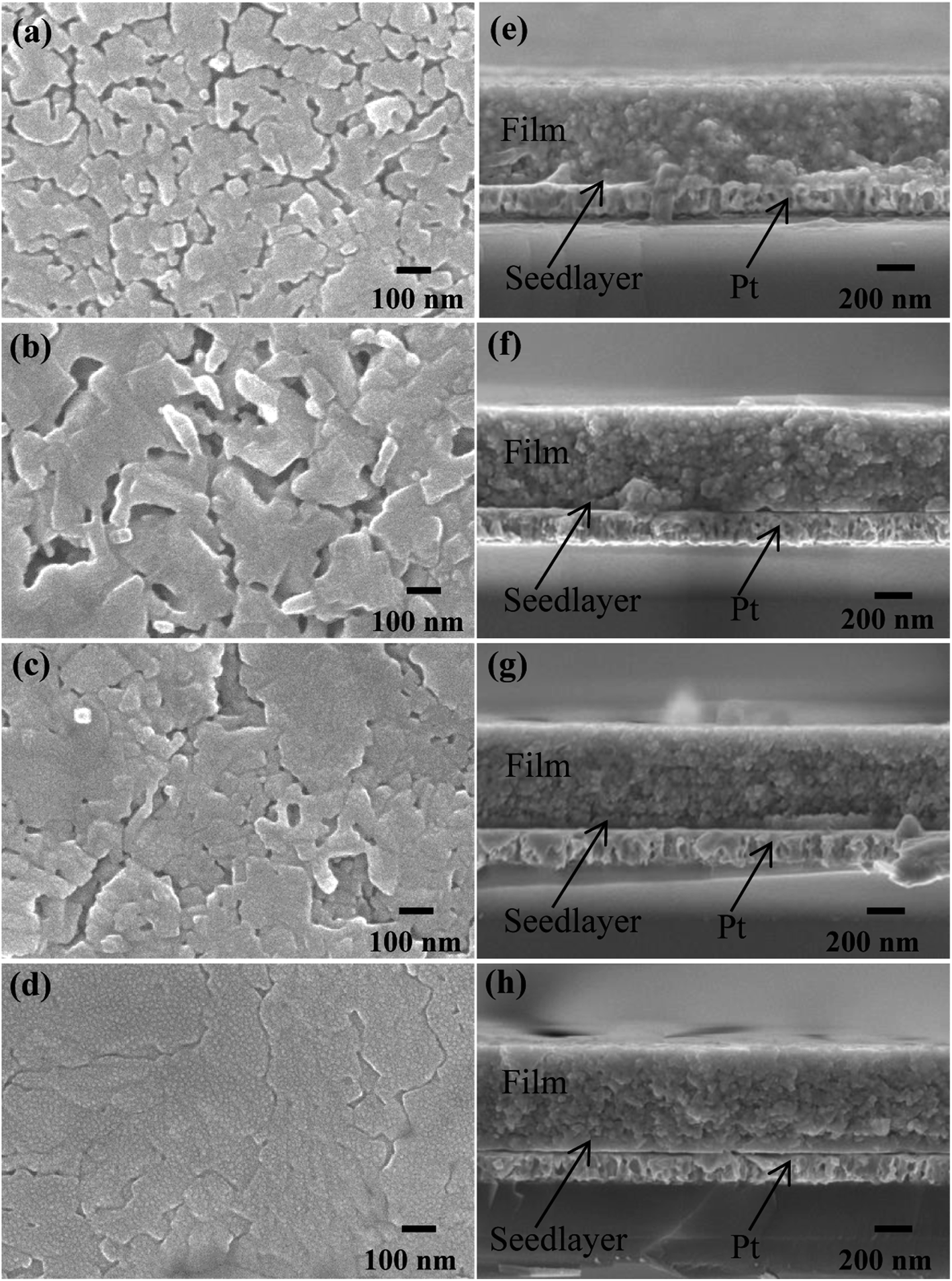 | ||
| Fig. 2 FESEM images of the BCZT thin films with (a) 10 nm-thick, (b) 20 nm-thick, (c) 30 nm-thick and (d) 40 nm-thick seed layers, cross-sectional FESEM images of the BCZT thin films with (e) 10 nm-thick, (f) 20 nm-thick, (g) 30 nm-thick and (h) 40 nm-thick seed layers. | ||
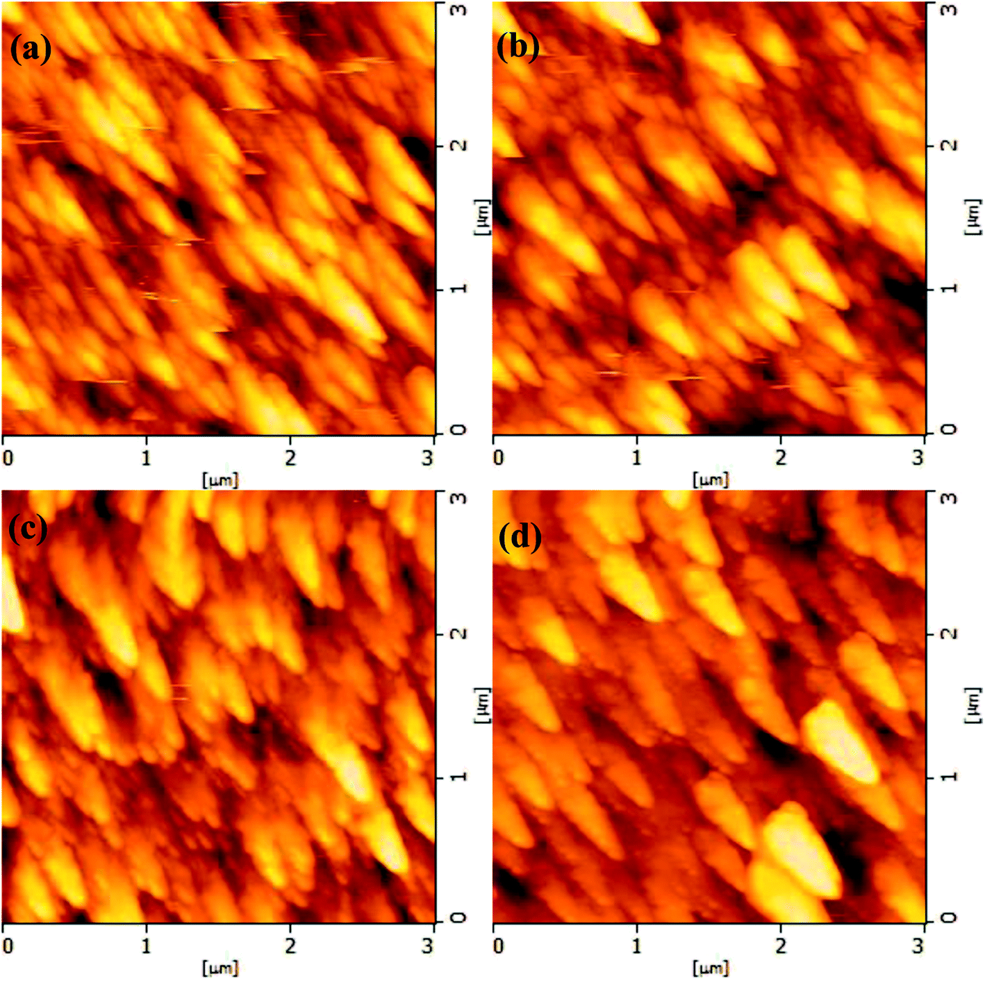 | ||
| Fig. 3 AFM topography images of the (a) 10 nm-thick, (b) 20 nm-thick, (c) 30 nm-thick and (d) 40 nm-thick crystallized BCZT seed layers on the substrate. | ||
Fig. 4 shows the dielectric constant and dielectric loss versus the applied electric field of the BCZT thin films with different seed layer thickness. The dielectric constant and loss exhibit butterfly shape, which due to the well-known ferroelectric hysteresis. Under zero bias, the dielectric constant ε(0) of BCZT thin films with 10 nm-thick, 20 nm-thick, 30 nm-thick and 40 nm-thick seed layer are 1260, 1130, 1100 and 740, respectively, which are more remarkable than that of BCZT thin films without seed layer.29 The dielectric constants decrease with the thickness of seed layer. Films prepared on Pt/Ti/SiO2/Si substrates at 700 °C could have increased titanium concentrations near the film/Pt interfaces, and the source is shown to be titanium diffusing from the substrate metallization stack.30 Each BCZT seed layer was heat treated at 700 °C for 5 min in this work, and thermal treatment times are 5 min, 10 min, 15 min, 20 min for the 10 nm-thick, 20 nm-thick, 30 nm-thick and 40 nm-thick seed layers, respectively. The thermal treatment times may induce different Ti gradients through the films and are responsible for the observed changes in film dielectric performance.31 The dielectric constant has strong field dependence, where typically the dielectric constant decreases with increasing field. At the bias electric field of 400 kV cm−1, the dielectric constant ε(v) of 900 render to tunability of 28.5%, defined as [ε(0) – ε(v)]/ε(0) × 100% for the film with 10 nm-thick seed layer. The tunability of BCZT thin films increase to the maximum value of 34.5% for the film with 20 nm-thick seed layer and then decrease with seed layer thickness. The ε(0) mainly contributes to the extrinsic response, while the ε(v) to the intrinsic response because of the suppressed extrinsic response under high electric field.32 The relative high tunability makes the films suitable for microwave and electrically tunable radio frequency applications.
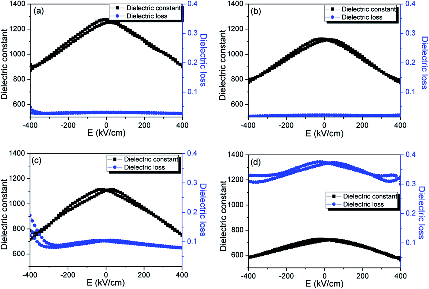 | ||
| Fig. 4 Dielectric constant and dielectric loss versus applied electric field of the BCZT thin films with (a) 10 nm-thick, (b) 20 nm-thick, (c) 30 nm-thick and (d) 40 nm-thick seed layers. | ||
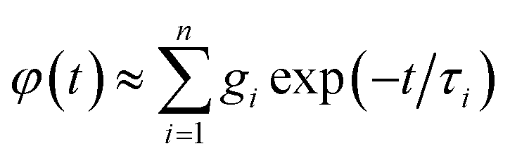
The dielectric constant and dielectric loss measured at room temperature as a function of frequency ranging from 1 kHz to 2 MHz for BCZT thin films with different seed layer thickness are shown in Fig. 5. The dielectric constants exhibit a slight decrease, whereas dielectric losses show an opposite tendency in the frequency range between 1 kHz and 2000 kHz. The frequency dispersion could be due to space charge polarization or Maxwell–Wagner type interfacial polarization.33 The space charge polarization is inherently related to the nonuniform charge accumulation near the interfaces between the film and electrode.34 Our experimental results on the thin film show quite interesting seed layer thickness dependence on dielectric properties as a function frequency. The drastic depressions in the dielectric constant at about ∼2 MHz, 1 MHz, 100 kHz and 10 kHz for the film with 10 nm-thick, 20 nm-thick, 30 nm-thick and 40 nm-thick seed layer associated with the relaxation of the dipole polarization, that is, to dipole fluctuations. It fits between the measured and calculated dielectric data for modified Kohlrausch Williams Watts properly which describe the dielectric relaxations in the normal and relaxor ferroelectric films.35 The dipole polarization (εdipole), the combined ionic and electronic polarizations (εionic+el.) and the combination (i.e., the total permittivity; εtotal) are quantified by the extended Debye function eqn (1) and (2)
 | (1) |
 | (2) |
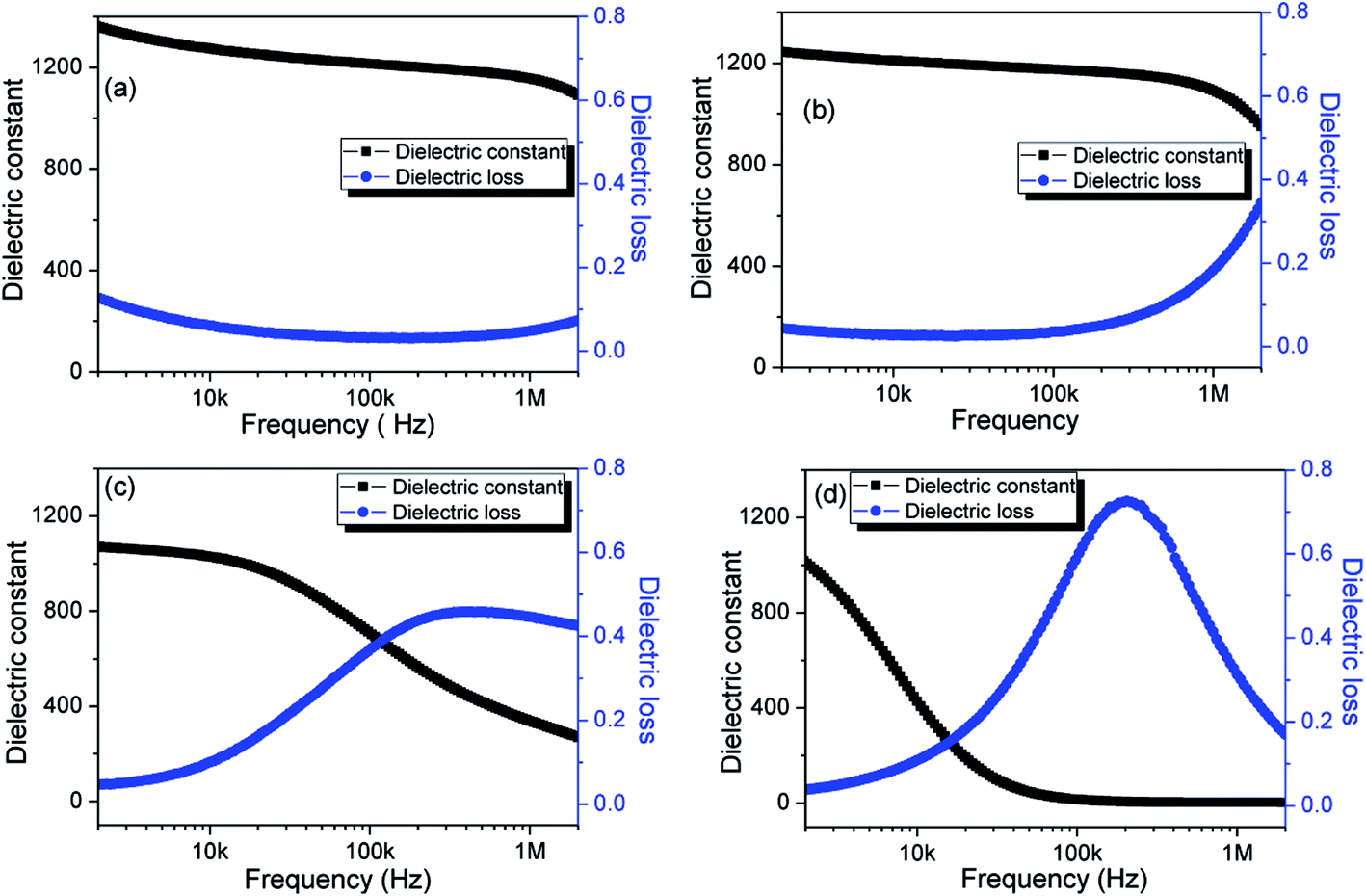 | ||
| Fig. 5 Dielectric constant and dielectric loss as a function of frequency of the BCZT thin films with (a) 10 nm-thick, (b) 20 nm-thick, (c) 30 nm-thick and (d) 40 nm-thick seed layers. | ||
The typical D–V loops and the corresponding d33–V loops of the BCZT thin films with different seed layer thickness are plotted in Fig. 6(a)–(d), respectively. The displacements of the BCZT thin films locate in the range of 0–0.5 nm calculated from the D–V curves, and the d33 values of the corresponding seed layer thickness (10 nm-thick, 20 nm-thick, 30 nm-thick and 40 nm-thick) thin films are 40 pm V−1, 60 pm V−1, 70 pm V−1 and 50 pm V−1, respectively. The BCZT thin films exhibiting good piezoelectric properties is due to the morphotropic phase boundary. Moreover, the d33 coefficients of BCZT thin films with seed layer are significantly improved compared with that of the thin films without seed layer (50 pm V−1).29 The larger grain size of the BCZT thin film with seed layer, which facilitate the domain to rotation, could contribute to the improvement of the d33 value. These results indicate that BCZT thin film with 30 nm-thick seed layer may be a promising candidate as lead free piezoelectric devices.
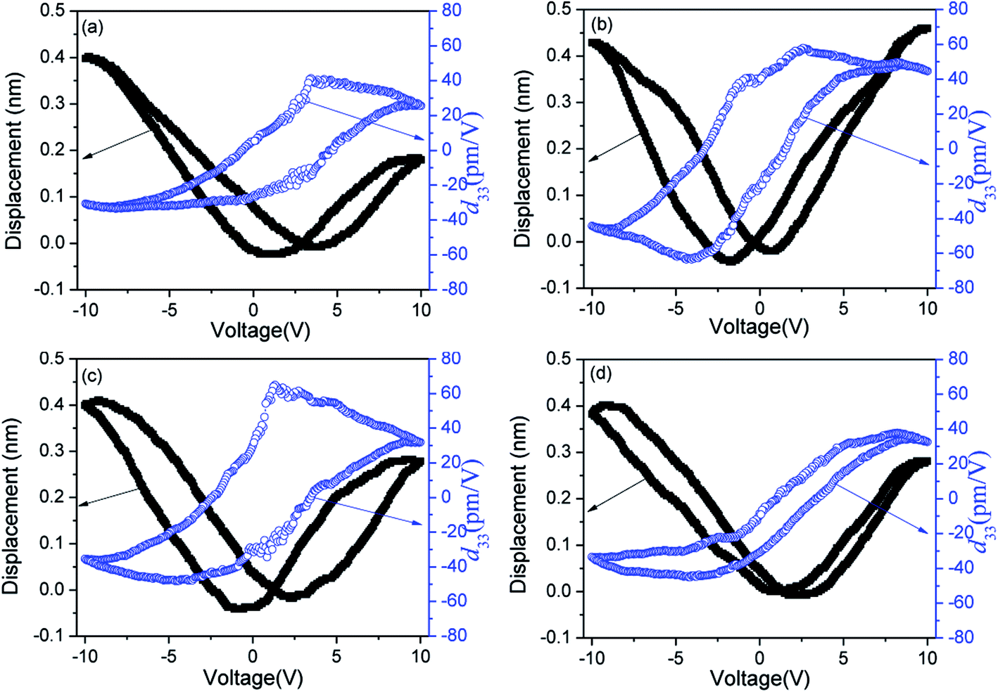 | ||
| Fig. 6 Electric field induced displacement and effective piezoelectric constant of the BCZT thin films with (a) 10 nm-thick, (b) 20 nm-thick, (c) 30 nm-thick and (d): 40 nm-thick seed layers. | ||
Conclusions
The BCZT thin films with 10 nm-thick, 20 nm-thick, 30 nm-thick and 40 nm-thick seed layer were prepared. The grain size increase from about 100 nm to 300 nm with the thickness of seed layer. The dielectric constant of BCZT thin films with 10 nm-thick, 20 nm-thick, 30 nm-thick and 40 nm-thick seed layer are 1260, 1130, 1100 and 740, respectively. The highest dielectric tunability of the BCZT thin films is 34.5%. The drastic depressions in the dielectric constant as a function of frequency associated with the relaxation of the dipole polarization are due to the grain size and increased titanium concentrations near the film/substrate interfaces. The highest effective piezoelectric coefficients is 70 pm V−1. The results indicated that the electric properties of films could be further improved by the configuration.Conflicts of interest
There are no conflicts to declare.Acknowledgements
This work was supported by the National Key R&D Program of China (grant No. 2016YFB0402701); the National Natural Science Foundation of China (grant No. 51502127), the Natural Science Foundation of Shandong Province of China (grant No. ZR2016EMM02 and ZR2014JL030) and the Science & Technology Innovation Program for Undergraduate (grant No. 201710447004 and 26312171908).References
- N. Izyumskaya, Y. I. Alivov, S. J. Cho, H. Morkoç, H. Lee and Y. S. Kang, Crit. Rev. Solid State Mater. Sci., 2007, 32, 111–202 CrossRef CAS
.
- S. Trolier-Mckinstry and P. Muralt, J. Electroceram., 2004, 12, 7–17 CrossRef CAS
- P. Muralt, J. Micromech. Microeng., 2000, 10, 136–146 CrossRef CAS
- X. J. Zheng, J. Y. Liu, J. F. Peng, X. Liu, Y. Q. Gong, K. S. Zhou and D. H. Huang, Thin Solid Films, 2013, 548, 118–124 CrossRef CAS
- W. Bai, D. Chen, P. Zheng, J. Xi, Y. Zhou, B. Shen, J. Zhai and Z. Ji, J. Eur. Ceram. Soc., 2017, 37, 2591–2604 CrossRef CAS
- L. Zhang, M. Zhang, L. Wang, C. Zhou, Z. Zhang, Y. Yao, L. Zhang, D. Xue, X. Lou and X. Ren, Appl. Phys. Lett., 2014, 105, 162908 CrossRef
- L. Jin, R. Huo, R. Guo, F. Li, D. Wang, Y. Tian, Q. Hu, X. Wei, Z. He, Y. Yan and G. Liu, ACS Appl. Mater. Interfaces, 2016, 8, 31109–31119 CAS
- L. F. Zhu, B. P. Zhang, X. K. Zhao, L. Zhao, P. F. Zhou and J. F. Li, J. Am. Ceram. Soc., 2013, 96, 241–245 CrossRef CAS
- W. Liu and X. Ren, Phys. Rev. Lett., 2009, 103, 257602 CrossRef PubMed
- W. Li, Z. Xu, R. Chu, P. Fu and G. Zang, Mater. Lett., 2010, 64, 2325–2327 CrossRef CAS
- D. Xue, Y. Zhou, H. Bao, C. Zhou, J. Gao and X. Ren, J. Appl. Phys., 2011, 109, 054110 CrossRef
- W. L. Li, T. D. Zhang, D. Xu, Y. F. Hou, W. P. Cao and W. D. Fei, J. Eur. Ceram. Soc., 2015, 35, 2041–2049 CrossRef CAS
- Y. Gong, H. Dong, X. Zheng, J. Peng, X. Li and R. Huang, J. Phys. D: Appl. Phys., 2012, 45, 305301 CrossRef
- J. Chen, H. Fan, X. Chen, P. Fang, C. Yang and S. Qiu, J. Alloys Compd., 2009, 471, L51–L53 CrossRef CAS
- Y. Wu, X. Wang, C. Zhong and L. Li, J. Am. Ceram. Soc., 2011, 94, 1843–1849 CrossRef CAS
- B. C. Luo, D. Y. Wang, M. M. Duan and S. Li, Appl. Phys. Lett., 2013, 103, 122903 CrossRef
- L. Shaohui, Z. Jiwei, W. Jinwen, X. Shuangxi and Z. Wenqin, ACS Appl. Mater. Interfaces, 2014, 6, 1533–1540 Search PubMed
- E. Gul, A. Stanulis, Y. Barushka, E. Garskaite, R. Ramanauskas, A. U. Morkan and A. Kareiva, J. Mater. Sci., 2017, 52, 12624–12634 CrossRef CAS
- S. Kunej, A. Veber and D. Suvorov, J. Am. Ceram. Soc., 2013, 96, 442–445 CAS
- L. Tang, J. Wang, J. Zhai, L. Bing Kong and X. Yao, Appl. Phys. Lett., 2013, 102, 142907 CrossRef
- W. Li, Q. Chi and W. Fei, J. Am. Ceram. Soc., 2011, 94, 1503–1508 CrossRef CAS
- C. Bhardwaj and D. Kaur, Curr. Appl. Phys., 2012, 12, 1239–1243 CrossRef
- J. Wu, Z. Fan, D. Xiao, J. Zhu and J. Wang, Prog. Mater. Sci., 2016, 84, 335–402 CrossRef CAS
- C. Zhong, X. Wang, Y. Wu and L. Li, J. Am. Ceram. Soc., 2010, 93, 3993–3996 CrossRef CAS
- W. Li, P. Li, H. Zeng, J. Hao and J. Zhai, Ceram. Int., 2015, 41, S356–S360 CrossRef CAS
- M. Sundararajan, L. John Kennedy, P. Nithya, J. Judith Vijaya and M. Bououdina, J. Phys. Chem. Solids, 2017, 108, 61–75 CrossRef CAS
- Y. Wu, X. Wang, C. Zhong and L. Li, J. Am. Ceram. Soc., 2017, 100, 3935–3942 CrossRef CAS
- X. Xu, G. Yuan, B. Xu, J. Yin, J. Liu, Z. Liu and G. L. Brennecka, J. Am. Ceram. Soc., 2015, 98, 2823–2828 CrossRef CAS
- W. Li, J. Hao, H. Zeng and J. Zhai, Curr. Appl. Phys., 2013, 13, 1205–1208 CrossRef CAS
- J. F. Ihlefeld, P. G. Kotula, B. D. Gauntt, D. V. Gough, G. L. Brennecka, P. Lu, E. D. Spoerke and N. Alford, J. Am. Ceram. Soc., 2015, 98, 2028–2038 CrossRef CAS
- C. T. Shelton, P. G. Kotula, G. L. Brennecka, P. G. Lam, K. E. Meyer, J.-P. Maria, B. J. Gibbons and J. F. Ihlefeld, Adv. Funct. Mater., 2012, 22, 2295–2302 CrossRef CAS
- W. Zhang, H. Cheng, Q. Yang, F. Hu and J. Ouyang, Ceram. Int., 2016, 42, 4400–4405 CrossRef CAS
- F. M. Pontes, E. R. Leite, E. Longo, J. A. Varela, E. B. Araujo and J. A. Eiras, Appl. Phys. Lett., 2000, 76, 2433–2435 CrossRef CAS
- N. Setter and R. Waser, Acta Mater., 2000, 48, 151–178 CrossRef CAS
- P. Dutta, S. Biswas and S. K. De, J. Phys.: Condens. Matter, 2001, 13, 9187–9196 CrossRef CAS
- T. Teranishi, S. Kajiyama, H. Hayashi and A. Kishimoto, J. Am. Ceram. Soc., 2017, 100, 1542–1550 CrossRef CAS
| This journal is © The Royal Society of Chemistry 2017 |