
 Open Access Article
 This Open Access Article is licensed under a
 Creative Commons Attribution 3.0 Unported Licence
Highly sensitive extended gate-AlGaN/GaN high electron mobility transistor for bioassay applications
Xiangzhen Ding ad,
Bin Miaoa,
Zhiqi Guag,
Baojun Wue,
Yimin Hue,
Hong Wange,
Jian Zhangf,
Dongmin Wu*a,
Wenhui Lu*b and
Jiadong Li*ac
ad,
Bin Miaoa,
Zhiqi Guag,
Baojun Wue,
Yimin Hue,
Hong Wange,
Jian Zhangf,
Dongmin Wu*a,
Wenhui Lu*b and
Jiadong Li*ac
ai-Lab, Suzhou Institute of Nano-Tech and Nano-Bionics, Chinese Academy of Sciences, Suzhou 215125, People’s Republic of China. E-mail: jdli2009@sinano.ac.cn; dmwu2008@sinano.ac.cn
bDepartment of Applied Physics, College of Science, Huzhou University, Huzhou 313000, People’s Republic of China. E-mail: whlv2016@189.cn
cState Key Laboratory of Applied Optics, Changchun Institute of Optics Fine Mechanics and Physics, Chinese Academy of Sciences, Changchun 130033, People’s Republic of China
dUniversity of Chinese Academy of Sciences, College of Materials Sciences and Opto-Electronic Technology, Beijing 100049, People’s Republic of China
eDivision of Nano-devices and Materials, Suzhou Institute of Nano-Tech and Nano-Bionics, Chinese Academy of Sciences (CAS), Suzhou 215123, People’s Republic of China
fNANO-X, Suzhou Institute of Nano-Tech and Nano-Bionics, Chinese Academy of Sciences, Suzhou 215125, People’s Republic of China
gSchool of Nano Technology and Nano Bionics, University of Science and Technology of China, Hefei, 230026, People’s Republic of China
First published on 11th December 2017
Abstract
Herein, an extended gate-AlGaN/GaN high electron mobility transistor (EG-AlGaN/GaN HEMT) with a high sensitivity for bioassay has been developed. The major difference between the EG-AlGaN/GaN HEMT transducer and a traditional AlGaN/GaN HEMT transducer is the sensing region. By extending the gate electrode and separating the sensing region from the channel of the AlGaN/GaN HEMT, our EG-AlGaN/GaN HEMT has a much larger sensing area and therefore achieves a low limit of detection (0.1 pg mL−1). Additionally, our transducer exhibits excellent linearity (R2 = 0.9934) with a wide range (from 0.1 pg mL−1 to 100 ng mL−1). We also demonstrate that the larger area of the extended sensing region can provide a larger current response of the transducer. The results give a proof-of-concept demonstration of the utilization of the EG-AlGaN/GaN HEMT for trace-level biological detection.
Introduction
Over the past few years, the field of biosensors based on ion-sensitive field effect transistors (ISFETs) has developed rapidly, which may assist humans in making point-of-care testing (PoCT) a reality.1,2 These ISFET based biosensors have exhibited marvellous properties, such as easier miniaturization, real-time and rapid responses, high sensitivity, compatibility with integrated circuit technology, and so on.1–3 On the other hand, the development of new materials broadens the diversity of the ISFET field. Recent studies of AlGaN/GaN HEMTs have explored their possible application in bioassays,4 on account of their high electron sheet carrier concentration, biocompatibility, lack of ion diffusion, and so forth.5 Plenty of work has been done to detect various biological analytes, such as cells,6 deoxyribonucleic acid,7 antigens,8,9 virus inhibitors,10 mercury ions (Hg2+),11 2,4,6-trinitrotoluene (TNT),12 etc.Just like with the ISFET based sensors, during the exploration of clinical applications, researchers found that there is a poor isolation between the device and the biological environment, which presents the issue of reliability, especially when the sensing surface is undergoing reiterative rinses.13–15 Moreover, the absence of electrical reproducibility and reliability limits the applications of FET based biosensors, as these are significant parameters with respect to sensors.13–15 To overcome these issues, the extended gate field effect transistor (EG FET) was proposed as a solution in 1983.16 This structure enables people to pursue a better electrical performance of the amplification component, independently of the tailored sensing component, and vice versa. Additionally, a much simpler encapsulation solution can be used to make the amplification component free from most of the undesirable interferences like light and temperature. Since then, this novel structure has proved quite useful for different fields like genetic analysis,17 immunoassay,18 urinalysis,19 and so on. However, to the best of our knowledge, this structure has not been demonstrated with AlGaN/GaN HEMTs, and so whether the EG-AlGaN/GaN HEMT will achieve a comparable level of electrical performance compared with the Au gate AlGaN/GaN HEMT8 or the biomolecule gate AlGaN/GaN HEMT9 needs to be studied.
In this work, we have investigated the feasibility of developing the EG-AlGaN/GaN HEMT for the detection of prostate specific antigen (PSA), which is considered to be the best biomarker for prostate cancer.20,21 A schematic illustration and plan view photomicrograph are shown in Fig. 1. The core of the EG-AlGaN/GaN HEMT is separated into two parts: the extended sensing region and the AlGaN/GaN HEMT. The area of the sensing region is as large as 700 μm × 700 μm, which will be shown to be quite useful for the signal amplification later.
 | ||
| Fig. 1 The structure of the EG-AlGaN/GaN HEMT: (A) a schematic illustration of the device, and (B) a plan view photomicrograph. | ||
Experimental
Sensor fabrication
To begin with, the nitride heterostructure used in this study consists of a 1.5 μm thick GaN buffer layer, an 18 nm thick AlGaN barrier layer and a 1.5 nm thick GaN cap layer, which were grown by metal organic chemical vapor deposition (MOCVD) on the sapphire substrate. The wafer was then pre-cleaned using piranha solution (H2SO4 and H2O2 with a volumetric ratio of 3![[thin space (1/6-em)]](https://www.rsc.org/images/entities/char_2009.gif) :1) and dried with nitrogen to ensure that it is clean. Inductively coupled plasma (ICP) etching with Cl2/BCl3 was performed to form the mesa isolation. The mesa height is around 40 nm to make sure that the etching surpasses the 2DEG layer. In order to remove the native oxide layer, the wafer was then dipped into 10% (by volume) hydrochloric acid for 60 seconds. Ohmic contacts were formed with the typical multilayer of Ti/Al/Ni/Au by e-beam evaporation and annealed by a rapid thermal processing system under a flow of ambient nitrogen at 880 °C for 45 seconds. To achieve an easier connection to the printed circuit board, the Ti/Ni/Au combination multilayer was evaporated overlapping above the ohmic contact electrode. A sputtering process was implemented to fabricate the gold extended gate. The wafer was encapsulated with SU8 except for the sensing region and connecting regions. After dicing, the separate devices were mounted and electrically connected to the printed circuit boards.
:1) and dried with nitrogen to ensure that it is clean. Inductively coupled plasma (ICP) etching with Cl2/BCl3 was performed to form the mesa isolation. The mesa height is around 40 nm to make sure that the etching surpasses the 2DEG layer. In order to remove the native oxide layer, the wafer was then dipped into 10% (by volume) hydrochloric acid for 60 seconds. Ohmic contacts were formed with the typical multilayer of Ti/Al/Ni/Au by e-beam evaporation and annealed by a rapid thermal processing system under a flow of ambient nitrogen at 880 °C for 45 seconds. To achieve an easier connection to the printed circuit board, the Ti/Ni/Au combination multilayer was evaporated overlapping above the ohmic contact electrode. A sputtering process was implemented to fabricate the gold extended gate. The wafer was encapsulated with SU8 except for the sensing region and connecting regions. After dicing, the separate devices were mounted and electrically connected to the printed circuit boards.
Sensor modification
After the devices were fabricated and encapsulated, surface modification was implemented. The sensing region, namely the gold extended gate, was cleaned in an ozone/UV chamber for 30 minutes in the first instance. Shortly after cleaning, the gold extended gate was immersed in deoxygenated cysteamine aqueous solution for 6 hours at room temperature, to form ubiquitous thiol–gold bonds, and then rinsed with deionized water. Glutaraldehyde solution with a concentration of 1.25% (by volume) was added into the lab-made reservoir for 2 hours to form a Schiff base between the aldehyde group and the amino group. Subsequently the device was rinsed with deionized water before the immobilization of 10 μg mL−1 PSA monoclonal antibody. The device was finally incubated at 4 °C for 24 hours, ready for the following measurements. The cysteamine and glutaraldehyde were purchased from Sigma-Aldrich Co. LLC. (Shanghai, China). The gold nanoparticle solution was purchased from Nanjing XFNANO Materials Tech Co., Ltd (Nanjing, China). All of the measurements were performed in phosphate-buffered saline solution (PBS).Results and discussion
Characterization
It has been well elucidated and demonstrated that there is a stable bond between amines and the surface of gold nanoparticles (Au NPs). This may stem from both the electrostatic adsorption between protonated amine groups and AuCl4−/AuCl2−, and a related complex of the form [AuCl(NH2R)].22 Hence, Au NPs can be utilized to demonstrate the presence of cysteamine. Fig. 2 shows images resulting from scanning electron microscopy (SEM). The Au NPs were uniformly distributed upon the surface of the gold platform after being rinsed over five times and sonicated, as shown in Fig. 2A, whilst adsorbed Au NPs are hardly observed with the absence of cysteamine, as shown in Fig. 2B. The corresponding diameter of the gold nanoparticles is around 20 nm.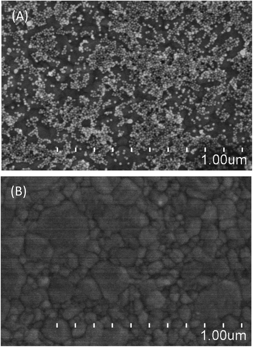 | ||
| Fig. 2 Characterization of the device: (A) the adsorption of gold nanoparticles in the presence of successfully modified cysteamine, and (B) non-adsorption in the absence of cysteamine. | ||
PSA detection
The device was finally connected to a Keithley 2636A instrument with a constant bias of 100 mV for the data acquisition. As shown in Fig. 3, the current response was quite steady in the first hundred seconds with the addition of 18 μL PBS, which indicates the stability of the device. Then, the current showed an instant abrupt decrease and then recovery to a steady level. This was due to the mechanical disturbance right after each step of titration by hand. For each cycle, within 60 seconds, the current achieved another steady level after completion of the antibody–antigen reaction. The obvious drop between every two titrations is around 100 nA. The red dashed lines in Fig. 3 depict the calculated average current during the steady stage, and the bold black line gives the fitted result of the real-time detection. At the end of the detection, a drop of PBS was titrated to verify the specificity of the device. The current response quickly returned to its previous level (i.e. at a PSA concentration of 100 ng mL−1). The device also shows good linearity with an R2 of 0.9934 in the inset, and the corresponding relationship is:| ΔI/ΔImax = −0.1658 × log([PSA]) + 0.7995 | (1) |
 | ||
| Fig. 3 The real-time detection of PSA (the red dashed lines are the average values and the bold black line is a fitted curve). | ||
Discussion of the sensing area
It was reported that the presence of a gold layer may degrade the performances of AlGaN/GaN HEMT transducers,23 however based on the above results, it appears to be less influential than we expected for the EG-AlGaN/GaN HEMT. The main factor of the EG-AlGaN/GaN HEMT which may enhance the device performance in this situation, we suppose, is the sensing area. This is because it was reported that more surface receptors lead to a better electrical parameter of sensitivity,24,25 and a larger sensing area has more receptors. In order to elucidate the relationship between the sensing area of the EG-AlGaN/GaN HEMT and its electrical characteristics, three different areas of the sensing pads were designed and modified (400 μm × 400 μm, 500 μm × 500 μm and 700 μm × 700 μm). The rest of the parameters of the EG-AlGaN/GaN HEMT are identical. With the exact same conditions of modification, target PSA with different concentrations in buffer solutions, including 0.1 pg mL−1, 1 pg mL−1, 10 pg mL−1, 100 pg mL−1, 1 ng mL−1, 10 ng mL−1, and 100 ng mL−1, were detected. The current changes (ΔI) of those three different sensing areas of the EG-AlGaN/GaN HEMT transducers for PSA detection were obtained. In order to minimize the influences caused by the modification, each group of experiments was repeated 3 times. As shown in Fig. 4, the statistical average results give a quite explicit conclusion, that a larger area of the extended gate leads to a larger current change in our transducer. Based on the above observation, we hypothesize that the larger area of the extended gate gives a larger total amount of surface charge which causes a larger change of the gate voltage due to the capacitance coupling. This explains why our EG-AlGaN/GaN HEMT exhibits good performance with a gold layer. | ||
| Fig. 4 The results of the current changes of three transducers with different sensing areas of the extended pads. The transducers were modified and measured with exactly the same conditions, and the experiments were repeated 3 times. (A) 400 μm × 400 μm, (B) 500 μm × 500 μm, and (C) 700 μm × 700 μm. | ||
Conclusions
In summary, we have developed a highly sensitive EG-AlGaN/GaN HEMT with a low limit of detection (0.1 pg mL−1). Furthermore, our transducer exhibits an outstanding electrical performance, including excellent linearity (R2 = 0.9934) with a wide range from 0.1 pg mL−1 to 100 ng mL−1. The device also shows stability and specificity in the presence of PBS. We also prove that a larger sensing area of the extended pad leads to a better electrical performance. It should also be noted that the extended gate can be tailored to various platforms for the corresponding detection of analytes, as long as the gate electrode is conductive. It is reasonable to believe that the EG-AlGaN/GaN HEMT will be a promising diagnostic tool for further PoCT applications.Conflicts of interest
There are no conflicts to declare.Acknowledgements
This work has been supported by the NSFC Project (No. 61573346 and 61104226), the Youth Innovation Promotion Association CAS (2014278) and the State Key Laboratory of Applied Optics.Notes and references
- P. Bergveld, IEEE Trans. Bio-Med. Electron., 1970, 17, 70–71 CrossRef CAS.
- C. S. Lee, S. K. Kim and M. Kim, Sensors, 2009, 9, 7111–7131 CrossRef CAS PubMed.
- A. de Moraes and L. Kubota, Chemosensors, 2016, 4, 20 CrossRef.
- R. Kirste, N. Rohrbaugh, I. Bryan, Z. Bryan, R. Collazo and A. Ivanisevic, Annu. Rev. Anal. Chem., 2015, 8, 149–169 CrossRef CAS PubMed.
- Y. Wang, P. Casal, S. C. Lee and W. Lu, Device Research Conference (DRC), 71st Annual, 2013 Search PubMed.
- G. Steinhoff, B. Baur, G. Wrobel, S. Ingebrandt, A. Offenhäusser, A. Dadgar, A. Krost, M. Stutzmann and M. Eickhoff, Appl. Phys. Lett., 2005, 86, 033901 CrossRef.
- B. S. Kang, S. J. Pearton, J. J. Chen, F. Ren, J. W. Johnson, R. J. Therrien, P. Rajagopal, J. C. Roberts, E. L. Piner and K. J. Linthicum, Appl. Phys. Lett., 2006, 89, 122102 CrossRef.
- B. S. Kang, H. T. Wang, T. P. Lele, Y. Tseng, F. Ren, S. J. Pearton, J. W. Johnson, P. Rajagopal, J. C. Roberts, E. L. Piner and K. J. Linthicum, Appl. Phys. Lett., 2007, 91, 112106 CrossRef.
- J.-d. Li, J.-j. Cheng, B. Miao, X.-w. Wei, J. Xie, J.-c. Zhang, Z.-q. Zhang and D.-m. Wu, J. Micromech. Microeng., 2014, 24, 075023 CrossRef.
- Y.-W. Kang, G.-Y. Lee, J.-I. Chyi, C.-P. Hsu, Y.-R. Hsu, C.-H. Hsu, Y.-F. Huang, Y.-C. Sun, C.-C. Chen, S. Chun Hung, F. Ren, J. Andrew Yeh and Y.-L. Wang, Appl. Phys. Lett., 2013, 102, 173704 CrossRef.
- J. Cheng, J. Li, B. Miao, J. Wang, Z. Wu, D. Wu and R. Pei, Appl. Phys. Lett., 2014, 105, 083121 CrossRef.
- Y. Guo, X. Wang, B. Miao, Y. Li, W. Yao, Y. Xie, J. Li, D. Wu and R. Pei, RSC Adv., 2015, 5, 98724–98729 RSC.
- Y. Hanazato, M. Nakako, S. Shiono and M. Maeda, IEEE Trans. Electron Devices, 1989, 36, 1303–1310 CrossRef CAS.
- A. S. Poghossian, Sens. Actuators, B, 1997, 44, 361–364 CrossRef CAS.
- L. T. Yin, J. C. Chou, W. Y. Chung, T. P. Sun and S. K. Hsiung, Sens. Actuators, B, 2000, 71, 106–111 CrossRef CAS.
- J. V. D. Spiegel, I. Lauks, P. Chan and D. Babic, Sens. Actuators, 1983, 4, 291–298 CrossRef.
- C. P. Chen, A. Ganguly, C. Y. Lu, T. Y. Chen, C. C. Kuo, R. S. Chen, W. H. Tu, W. B. Fischer, K. H. Chen and L. C. Chen, Anal. Chem., 2011, 83, 1938–1943 CrossRef CAS PubMed.
- M. Kamahori, Y. Ishige and M. Shimoda, Biosens. Bioelectron., 2007, 22, 3080–3085 CrossRef CAS PubMed.
- W. Guan, X. Duan and M. A. Reed, Biosens. Bioelectron., 2014, 51, 225–231 CrossRef CAS PubMed.
- D. A. Healy, C. J. Hayes, P. Leonard, L. McKenna and R. O’Kennedy, Trends Biotechnol., 2007, 25, 125–131 CrossRef CAS PubMed.
- M. A. Najeeb, Z. Ahmad, R. A. Shakoor, A. M. A. Mohamed and R. Kahraman, Talanta, 2017, 168, 52–61 CrossRef CAS PubMed.
- A. Kumar, S. Mandal, P. R. Selvakannan, R. Pasricha, A. B. Mandale and M. Sastry, Langmuir, 2003, 19, 6277–6282 CrossRef CAS PubMed.
- M. Wirde, U. Gelius and L. Nyholm, Langmuir, 1999, 15, 6370–6378 CrossRef CAS.
- M. S. Makowski, I. Bryan, Z. Sitar, C. Arellano, J. Xie, R. Collazo and A. Ivanisevic, Appl. Phys. Lett., 2013, 103, 13701 CrossRef PubMed.
- Y. Xin, B. Munge, V. Patel, G. Jensen, A. Bhirde, J. D. Gong, N. K. Sang, J. Gillespie, J. S. Gutkind and F. Papadimitrakopoulos, J. Am. Chem. Soc., 2006, 128, 11199–11205 CrossRef PubMed.
| This journal is © The Royal Society of Chemistry 2017 |