
 Open Access Article
 This Open Access Article is licensed under a
 Creative Commons Attribution 3.0 Unported Licence
TiO2 nanorod arrays hydrothermally grown on MgO-coated compact TiO2 for efficient perovskite solar cells
Wenhan Chen,
Qi Luo,
Xueshuang Deng,
Jianfeng Zheng,
Chenxi Zhang,
Xiaohong Chen and
Sumei Huang *
*
Engineering Research Center for Nanophotonics & Advanced Instrument, Ministry of Education, School of Physics and Materials Science, East China Normal University, North Zhongshan Rd. 3663, Shanghai 200062, P. R. China. E-mail: smhuang@phy.ecnu.edu.cn; Fax: +86 21 62234321
First published on 24th November 2017
Abstract
The morphology of electron transport layers has a significant impact on the device architecture and electronic processes of mesoscopic perovskite solar cells (PSCs). In this study, ultrathin MgO is coated on the surface of compact TiO2 (c-TiO2). The MgO-coated c-TiO2 is first used as seeds to hydrothermally grow one-dimensional (1D) TiO2 nanorod (NR) arrays for PSC devices. Rutile nanorod arrays are fabricated via a facile solvothermal method using tetrabutyl titanate (TBT) as the Ti precursor. The microstructures and morphologies, including nanorod diameter, length, and areal density, of the TiO2 NR arrays are varied by controlling the concentration of TBT from 0.3 M to 0.7 M. Furthermore, the profound effects of the MgO modification and titania nanorod morphology on the pore-filling of perovskite CH3NH3PbI3, charge separation and recombination at the perovskite/titania nanorod interface are investigated. Our results reveal that the Ti precursor concentration strongly affects the open-circuit voltage (VOC), short-circuit current density (JSC), and fill factor (FF) of the 1D TiO2 NR array-based device. Under optimized conditions with MgO coating and at 0.4 M TBT, our champion cell with 1D TiO2 NRs demonstrates a power conversion efficiency (PCE) of 17.03% with JSC = 22.01 mA cm−2, VOC = 1.06 V, and FF = 0.73. Under the same fabrication conditions, MgO modification enhances the average PCE to 16.24% for the PSCs with the MgO coating from 13.38% for the PSCs without the MgO coating. The devices show an approximately 18% improvement in performance, which mainly results from the open-circuit voltage and fill factor enhancements. Moreover, advantageously, the MgO modification is found to reduce the current density–voltage (J–V) hysteresis with respect to the scan direction and improve the UV stability of the non-encapsulated cells. Therefore, this study presents a promising approach to fabricate efficient and stable one-dimensional TiO2 nanorod array-based perovskite solar cells.
1. Introduction
Organometal halide perovskite solar cells (PSCs) are becoming a significant portion of photovoltaic technologies due to their low cost and rapidly increasing efficiency. PSCs have already surpassed organic photovoltaics (OPVs)1 and dye-sensitized solar cells (DSSCs)2,3 and are now, at least in terms of efficiency, in the same range as leading thin film PVs such as cadmium telluride (CdTe)4 and copper indium gallium selenide (CIGS)5,6 or other types of thin film solar cells that have existed for decades. Currently, perovskite solar cells based on zero dimensional (0D) metal oxide nanostructures have achieved excellent power conversion efficiencies (PCEs) of 22.1% (for small area devices)7 and 17.8% (for large area devices).8 The major components of PSC devices include electron transporting layers (ETL), hole transporting layers (HTL) and perovskite absorbing films. Among these functional layers, ETLs are a critical component of PSCs for the improvement in PV performance.9 Mesoporous TiO2 is the most common ETL used for highly efficient perovskite solar cells.10–15 The mesoporous architecture is comprised of a large number of ca. 20 nm-sized nanoparticles (NPs) with many grain boundaries, which hamper electron transport and limit the charge collection efficiency.16,17 In addition, due to the random distribution of NPs within mesoporous metal oxide films, pore-filling of perovskite and hole transport materials (HTM) in the interspace between NPs remains a persistent difficulty. To overcome the problems associated with mesoscopic structures, great effort is being devoted towards the application of one-dimensional (1D) ETLs in PSCs. ETLs with 1D structures provide a direct path for the transport of photo-generated electrons. These structured ETLs also allow better pore filling of the perovskite absorber than mesoscopic TiO2 films due to the open and regular pore structure of the former.18–20 TiO2, WO3, ZnO and CdS nanorods and nanotubes have been tested as ETLs for PSCs, but only TiO2 nanorods have consistently produced PSCs with PCEs above 15%.21–23 TiO2 nanorods (NRs) are developing as another popular configuration for ETLs in perovskite solar cells. Qiu et al.19 first reported the use of TiO2 nanorods as an ETL in PSCs. Using a CH3NH3PbBr3 absorber on 1.5 μm-thick nanorods, they reported a PCE of 4.87%. This report triggered new research on the application of TiO2 nanorods as an ETL for perovskite solar cells. Kim et al.20 made comparative studies on the performance of longer and shorter TiO2 nanorods. They concluded that shorter nanorods could provide better infiltration of perovskite. Using 560 nm-long nanorods, they achieved a PCE of about 9.4%. In 2014, Jiang et al.24 fabricated a perovskite solar cell using 900 nm-long TiO2 nanorods as the ETL and achieved an efficiency of 11.7%. Subsequently, Mali et al.25 were able to demonstrate a TiO2-nanorod based perovskite solar cell with an efficiency of 13.5%, which was achieved by passivating the surface of the nanorods with ultrathin TiO2 via atomic layer deposition in 2015. Most recently, in 2016, Li et al. achieved record efficiencies of 18.22%.26 They utilized a UV-ozone cleaning process to eliminate organic residues on the nanorod surface to improve the TiO2 nanorod/perovskite interface.In this study, ultrathin MgO is coated on the surface of compact TiO2 (c-TiO2). The MgO-coated c-TiO2 is first used as seeds to hydrothermally grow one-dimensional (1D) TiO2 nanorod (NR) arrays for PSC devices. Rutile nanorod arrays are fabricated via a facile solvothermal method using tetrabutyl titanate (TBT) as the Ti precursor. The microstructures and morphologies of the TiO2 NR arrays, including nanorod diameter, length and areal density, are tuned by controlling the concentration of TBT from 0.3 M to 0.7 M. The electrical behavior and optical properties of titania nanorod ETLs are characterized and examined to understand the sources of both underperformance and outperformance in various device parameters. We demonstrate the profound effect of the MgO modification and titania nanorod morphology on the pore-filling of perovskite CH3NH3PbI3, charge separation and recombination at the perovskite/titania nanorod interface. We optimize the Ti precursor concentration and morphology of the hydrothermally grown TiO2 nanorod arrays to produce hysteresis-less CH3NH3PbI3 perovskite solar cells with a champion PCE of 17.03% and high UV light stability.
2. Experimental
2.1 Materials
Tetrabutyl titanate (TBT) (99.0%), titanium(IV) isoproxide (99.999% metal basis) and magnesium acetate tetrahydrate (99.98% metal basis) were obtained from Aladdin. Hydrochloric acid (AR) was obtained from Sinopharm Chemical Reagent Co., China. All reagents were used as received without further purification.2.2 Preparation of rutile TiO2 nanorod arrays
Rutile TiO2 arrays were prepared via a hydrothermal method, as reported in ref. 27. Fluorine-doped tin oxide (FTO)-coated glass substrates were cleaned by ultrasonication with soap, deionized water, acetone, and isopropyl alcohol and finally treated with ultraviolet light for about 20 minutes. Then, isopropyl titanate (200 μL) and ethanol (5 mL) were mixed to prepare a clear precursor sol. The precursor sol was spin-coated on the Zn/HCl-etched FTO substrate at 4500 rpm, followed by annealing at 500 °C to form a compact TiO2 (c-TiO2) layer. To prevent charge recombination at the methylamine lead iodide/TiO2 interface in perovskite solar cells, MgO coated c-TiO2 layers were fabricated before the synthesis of TiO2-NR arrays by modifying the procedure reported in our previous work.14 An MgO precursor solution of Mg(CH3COO)2 in deionized water was spin-coated on the c-TiO2 layer at 4500 rpm for 30 seconds, and was then heated at 400 °C for 1 h. The concentration of the magnesium salt used was 70 mM. Herein, two pieces of clean FTO glass with TiO2 seed layers were placed at an angle of 45° against the wall of the Teflon-liner with the conducting side facing down. Concentrated hydrochloric acid (36.5–38% by weight) was added to deionized water with a volume ratio of 1![[thin space (1/6-em)]](https://www.rsc.org/images/entities/char_2009.gif) :1 and stirred for 2 minutes. Subsequently, TBT was added, and the mixture was further stirred. The amount of titanium butoxide was set as 0.03, 0.035, 0.04, 0.05, 0.06 M to obtain the desired TiO2-NR arrays respectively. The hydrothermal synthesis was conducted at 150 °C for 4 h in an electric oven to ensure that TiO2-NR arrays with a uniform thickness were obtained. After cooling to room temperature in air, the films were taken out from the autoclaves, rinsed with deionized water, dried in air, and annealed at 500 °C for 30 min to remove any residual organic contaminants.
:1 and stirred for 2 minutes. Subsequently, TBT was added, and the mixture was further stirred. The amount of titanium butoxide was set as 0.03, 0.035, 0.04, 0.05, 0.06 M to obtain the desired TiO2-NR arrays respectively. The hydrothermal synthesis was conducted at 150 °C for 4 h in an electric oven to ensure that TiO2-NR arrays with a uniform thickness were obtained. After cooling to room temperature in air, the films were taken out from the autoclaves, rinsed with deionized water, dried in air, and annealed at 500 °C for 30 min to remove any residual organic contaminants.
2.3 Solar cell device fabrication
CH3NH3PbI3 was coated on the TiO2-NR arrays via a typical one-step spin-coating procedure under a nitrogen atmosphere.28,29 Synthesized CH3NH3I (0.1975 g) powder and lead iodide PbI2 (0.5785 g) were stirred in a mixture of γ-butyrolactone (GBL) (700 μL) and dimethylsulphoxide (DMSO) (300 μL) at 60 °C for 12 h. The film was spin-coated with the precursor solution at 2000 rpm for 30 seconds and at 3500 rpm for 40 seconds. 70 μL of anhydrous diethyl ether was dropped onto the center of the sample during the last 30–40 s. The CH3NH3PbI3 film was obtained after annealing at 115 °C for 20 min on a hotplate, and the film color changed from transparent to yellow and finally to dark brown. After the deposition of perovskite, an HTM solution was spin-coated at 3500 rpm for 30 s. The HTM solution was obtained using 1 mL 2,2,7,7-tetrakis(N,N-di-p-methoxyphenylamine)-9,9-spirobifluorene (spiro-OMeTAD)/chlorobenzene (72.3 mg mL−1) solution with 17.5 μL Li-TFSI/acetonitrile (520 mg mL−1) and 28.8 μL tBP. Finally, an Ag–Al electrode (70 nm) was thermally evaporated at an atmospheric pressure of 10−7 Torr to match the work function.29,302.4 Characterization
The morphology, structure and composition of the TiO2 arrays were investigated via field emission scanning electron microscopy (FESEM, HitachiS-4800), and X-ray diffraction (XRD, Bruker D8 Davinci instrument, Cu-Kα: λ = 0.15406 nm). UV-vis absorption spectra were obtained using a UV-vis spectrophotometer (HitachiU-3900). The photocurrent density-voltage (J–V) curve was measured using a Keithley model 2440 Source Meter under the illumination of simulated AM 1.5 G solar light (100 mW cm−2, 1 sun intensity) from a Newport solar simulator system (equipped with a 1 kW xenon arc lamp, oriel, calibrated with a standard silicon reference cell). During device photovoltaic performance characterization, a metal aperture mask with an opening of about 0.09 cm2 was used. External quantum efficiency (EQE) measurements (74125, Oriel, USA) were also carried out for these cells.3. Results and discussion
Fig. 1 shows the top surface and cross-sectional SEM images of the TiO2 NR arrays prepared with different concentrations of TBT ranging from 0.03 M to 0.07 M. The TiO2-NR arrays are grown in the preferred [001] direction, and are vertically and uniformly distributed on the glass/FTO/c-TiO2 substrates. Hydrothermal solution growth of TiO2-NR arrays has been widely reported on TiO2 seed layers or directly on Ti foil substrates to increases the nucleation sites for growth.18,31,32 In our work, the growth mechanism of the TiO2-NR arrays on MgO-coated c-TiO2 is similar to the traditional case due to the ultrathin thickness of MgO. When TBT was mixed with HCl solution at room temperature, TBT reacted with HCl and H2O forming a Ti(IV) complex. When the solution was heated at 150 °C, the Ti(IV) complex transformed into TiO2 on the surface of the c-TiO2 layer. Cl− ions can selectively adsorb onto the (110) crystal planes suppressing further growth of the planes, resulting in anisotropic growth along the [001] orientation18,31 Meanwhile, the growth process was significantly influenced by the concentration of the Ti(IV) complex in the solution. As shown in Fig. 1, the diameter and areal density of the TiO2 NRs changed with the concentration of TBT. As the TBT concentration increased from 0.03 M to 0.07 M, the length and mean diameter (measured by Nano Measurer) of the TiO2-NRs increased from 250 nm and 21 nm to 1163 nm and 76 nm, respectively, while the areal density (number of nanorods per unit area) of the TiO2-NR arrays increased from 224 μm2 at 0.03 M TBT to 392 μm2 at 0.04 M, and then decreased as the TBT concentration further increased, as shown in Table 1. The TiO2-NR arrays became more and more vertically aligned and compact with an increase in the TBT concentration from 0.03 M to 0.07 M. It is worth noting that the TiO2-NR arrays grown in 0.04 M TBT precursor solution were 298 nm in length and had a small mean diameter of 22 nm and high areal density of 392 μm2. The microstructures and morphologies of the grown TiO2-NR arrays play an important role in the performance of PSCs due to the charge separation and recombination at the perovskite/titania nanorod interface19,26 and the sensitivity of perovskite crystallization to the interfacial structure.33,34 A small diameter is very important in obtaining a high area density, which is conducive to increasing the surface area of the TiO2-NR array. Increasing the surface area leads to improved charge separation at the interface of CH3NH3PbI3/TiO2. On the other hand, with an increase in length of the TiO2 NRs, the charge combination is expected to be intensified.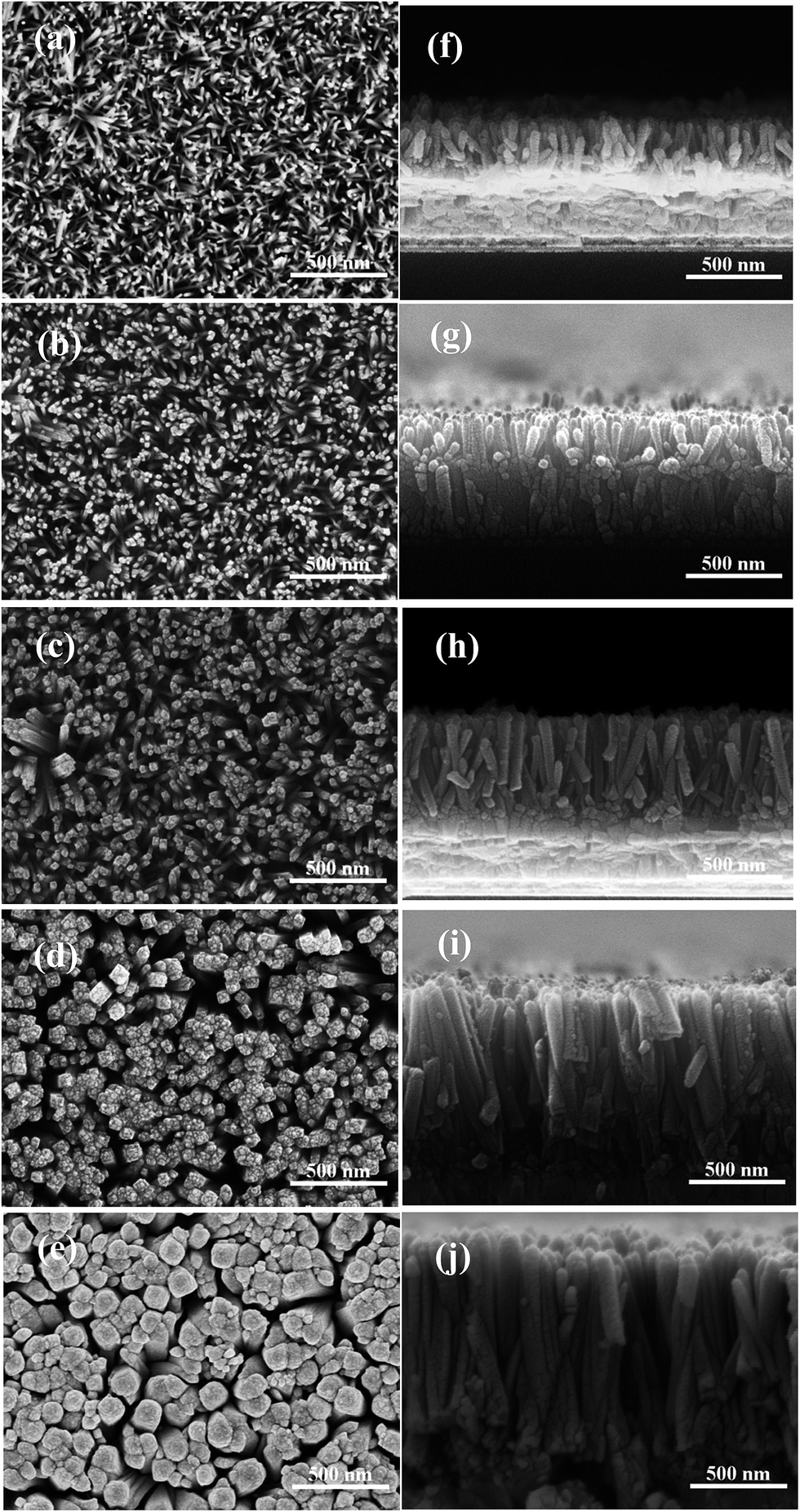 | ||
| Fig. 1 Top surface and cross-sectional SEM images of TiO2-NR arrays prepared with different concentrations of TBT, (a and f) 0.03 M, (b and g) 0.04 M, (c and h) 0.05 M, (d and i) 0.06 M and (e and j) 0.07 M. | ||
| TBT concentration | Length (nm) | Absorber length (nm) | Diameter (nm) | Areal density (μm−2) | |
|---|---|---|---|---|---|
| Max | Mean | ||||
| 0.03 M | 250 | 401 | 35 | 21 | 224 |
| 0.04 M | 298 | 452 | 36 | 22 | 392 |
| 0.05 M | 555 | 720 | 55 | 33 | 276 |
| 0.06 M | 906 | 1107 | 89 | 59 | 120 |
| 0.07 M | 1163 | 1317 | 161 | 76 | 112 |
Fig. 2 shows top surface and cross-sectional SEM images of the CH3NH3PbI3-coated TiO2-NR arrays prepared with different concentrations of TBT. It can be seen that the total thickness of the CH3NH3PbI3 absorber layer on the TiO2-NR arrays prepared with TBT concentrations ranging from 0.03 M to 0.07 M increased from about 400 nm to 1320 nm. The pore-filling of CH3NH3PbI3 dramatically varied together with a change in the interspace between the TiO2 NRs. The dispersed small sized TiO2 NRs prepared with a low TBT concentration facilitated the loading of perovskite into the TiO2 pores or clearance between TiO2 NRs. The perovskite capping layers in the TiO2-NR arrays prepared with the low TBT concentrations of 0.03 M and 0.04 M show a very smooth and compact top surface morphology, as shown in Fig. 2(a) and (b), respectively. However, when the TBT concentration is higher, some perovskite material voids are visible on the top surface of the perovskite absorber, as shown in Fig. 2(d) and (e). Moreover, from the side views (Fig. 2(h)–(j)), large perovskite material voids are clearly observed on the surface or vicinity of the TiO2 NRs, which is probably caused by an Ostwaldt type ripening process during the crystal growth.35
 | ||
| Fig. 2 Top surface and cross-sectional SEM images of the CH3NH3PbI3-coated TiO2-NR arrays prepared with different concentrations of TBT, (a and f) 0.03 M, (b and g) 0.04 M, (c and h) 0.05 M, (d and i) 0.06 M and (e and j) 0.07 M. | ||
The pinholes or perovskite material voids in the absorbers can decrease the shunt resistances or lead to HTM infiltration and cause short circuit, resulting in poor PSC device performances. Notably, the absorber sample formed under condition of 0.04 M TBT shows the optimal top-view and cross-section morphological properties. The perovskite semiconductor material almost completely covers the TiO2 NR array scaffold in this case, as shown in Fig. 2(g).
Fig. 3(a) and (b) show the UV-vis spectra of the bare and CH3NH3PbI3 coated TiO2-NR arrays prepared with different concentrations of TBT, respectively. From Fig. 3(a), the absorption onsets of the TiO2-NR arrays prepared with TBT concentrations of 0.03 M (0.04 M), 0.05 M, and 0.06 M (0.07 M) are approximately 360 nm, 400 nm and 405 nm, respectively. Consistent with the SEM images shown in Fig. 1, the results of the UV-vis spectra are thought to be attributed to the increasing length and diameter of the TiO2 nanorod arrays, which may reduce reflection and transmission.36 The real absorption spectra of perovskite CH3NH3PbI3 is shown in Fig. 3(c). As can be seen from Fig. 3(c), with the increase in TBT concentration from 0.03 to 0.04 M, the perovskite CH3NH3PbI3 has gradually stronger absorption in the 450–750 nm wavelength range. However, when the TBT concentration increased further from 0.04 to 0.07 M, the perovskite has weaker absorption. The perovskite film formed with the TBT concentration of 0.04 M exhibits the strongest light absorption over the 450–750 nm wavelength range. The increased absorption of the perovskite should be the result of improved surface coverage and more uniform crystal formation in the perovskite thin film. Moreover, due to the similar thicknesses of the CH3NH3PbI3 capping layers under the conditions of various TBT concentrations, as shown in Fig. 2(f)–(j), the increased absorbance is mainly associated with the optimized interfaces of perovskite/TiO2-NRs.
 | ||
| Fig. 3 UV-vis spectra of (a) TiO2 NRs, (b) CH3NH3PbI3-coated TiO2 NRs with different concentrations of TBT, and (c) absorber layers obtained by subtracting the TiO2 NRs contribution from the CH3NH3PbI3 coated TiO2 NRs. | ||
Fig. 4(a) and (b) show the current density–voltage (J–V) characteristics and EQE spectra of the fabricated devices based on 1D TiO2 NRs prepared with different TBT concentrations. The J–V measurements were recorded under AM 1.5 G solar irradiance, and the photovoltaic performance parameters and shunt (RSH) and series (RS) resistances are summarized in Table 2. It can be seen that the PSC device based on TiO2 NRs prepared with a TBT concentration of 0.03 M shows a PCE of 14.55%, resulting from an open circuit voltage (VOC) of 1.05 V, current density (JSC) of 22.0 mA cm−2 and fill factor (FF) of 0.63. When the TBT concentration was increased from 0.03 to 0.04 M, the device showed a significant improvement in FF with the corresponding increase in PCE to 16.24%. Upon further increasing the TBT concentration from 0.04 M to 0.07 M, lower JSC, VOC and FF values, and thus worse PV performances were observed in the related devices. At 0.07 M TBT, a considerable decrease in JSC, VOC and FF was observed, resulting in the corresponding decrease in PCE to 13.52%. From Tables 1 and 2, when the TBT concentration increased from 0.04 M to 0.07 M, the length of the grown TiO2-NRs increased from 250 nm to 1163 nm, while the JSC, VOC, FF and PCE values of the device performance continuously decreased. These results can be attributed to the disorder in the longer nanorod arrays and reduced pore-filling (Fig. 2). Kim et al. also found that photocurrent, photovoltage and power conversion efficiency decreased with an increase in nanorod length from 0.56 μm to 1.58 μm.20
 | ||
| Fig. 4 (a) J–V characteristics and (b) EQE spectra of the PSC devices based on TiO2-NR arrays prepared with different TBT concentrations. | ||
| TBT amount (M) | VOC (V) | JSC (mA cm−2) | Fill factor | PCE (%) | RS (Ω) | RSH (Ω) |
|---|---|---|---|---|---|---|
| 0.03 | 1.05 | 22.0 | 0.63 | 14.55 | 104 | 49137 |
| 0.04 | 1.04 | 21.75 | 0.73 | 16.24 | 40 | 20430 |
| 0.05 | 1.01 | 21.23 | 0.70 | 14.90 | 43 | 14104 |
| 0.06 | 1.02 | 20.66 | 0.69 | 14.69 | 42 | 11802 |
| 0.07 | 0.98 | 19.25 | 0.68 | 13.52 | 41 | 9800 |
For solar cells, the shunt resistance (RSH) is due to p–n junction non-idealities and impurities near the junction; however, the major contributors to the series resistance (RS) are the bulk resistance of the semiconductor material (the active layer), the contact resistance at the semiconductor–conductive interfaces and the resistance of the conductive contacts.37 As the TBT concentration increased from 0.03 to 0.04 M, the device showed an obvious decrease in both RS and RSH. Further increasing the TBT concentration from 0.04 M to 0.07 M, RS changed slightly, while RSH continuously decreased. At 0.07 M TBT, the shunt resistance decreased by 5 times. The lowest FF of the device prepared at 0.03 M can be associated with the largest RS.38 The key limitation in the performance of meso-superstructured PSCs is the balance between RSH and RS resistance.28 Both the smallest series resistance and the second largest shunt resistance of the PSC device prepared at 0.04 M are responsible for its highest FF. When the TBT concentration is 0.04 M, the formed TiO2 NRs have a small diameter and the highest area density, which are conducive to increasing the surface area of the TiO2-NR arrays and enhancing pore-filling. This leads to improved charge separation at the interface of CH3NH3PbI3/TiO2, and as a result, optimal and high-performance perovskite solar cells were assembled.
The EQE values of the devices based on the TiO2 NRs prepared with various TBT concentrations are quite different in the wavelength range of 300 and 400 nm, as shown in Fig. 4(b). This difference is due to the absorption of light by the TiO2 NRs, as shown in Fig. 3(a). Moreover, the EQE shown in Fig. 4(b) is relatively higher for the lower TBT concentration in the wavelength range of 400 and 600 nm, which indicates that the shorter nanorods utilize light more efficiently than the longer nanorods in this wavelength region. The EQE results of the devices with different TBT amounts are in good agreement with that from the J–V measurements of these cells, as shown in Fig. 4(a).
In early-reported TiO2 NR array based PSCs,19,20,24–26 TiO2 NR arrays were mostly grown on TiO2 compact-layer seeded FTO substrates via the hydrolysis of Ti precursors. In our work, ultrathin MgO coated-c-TiO2 layers were fabricated before the synthesis of the TiO2-NR arrays by modifying the procedure reported in our previous work for incorporating MgO into porous TiO2.14 In order to examine the influence of MgO modification, we measured the top surface and cross-sectional SEM images of TiO2 NR arrays directly deposited on c-TiO2 with 0.04 M TBT, as shown in Fig. 5(a) and (b), respectively. The length and mean diameter of the TiO2 nanorods prepared at 0.04 M TBT without MgO modification are similar to that of the TiO2 NRs grown at the same TBT concentration with MgO modification; however, the areal density of the former (248 μm−2) is smaller than that (392 μm−2) of the latter, as shown in Fig. 5 and 1(b) and (g), respectively. Moreover, without MgO modification, the obtained TiO2 NR arrays are randomly and non-uniformly tilted. The small areal density and badly aligned and unevenly distributed TiO2 NR arrays hinder infiltration of perovskite, thus leading to absorbers with poor morphology which degrade the photovoltaic performance of PSCs.20,24,39 Furthermore, it is known that there are numerous pin-holes present within TiO2 compact layers prepared via solution methods and these pin-holes expose the FTO gains underneath the layers, which decreases the blocking capability and electron collecting efficiency of the photoanode.40,41 With MgO modification of the c-TiO2, MgO insulating material particles are spread over the c-TiO2 layer which can partially cover these pores. Furthermore, since MgO particles are scattered over the substrate, the MgO coated c-TiO2 layer has places where TiO2 can have electrical contact with the TiO2 NRs and perovskite. Upon MgO modification, the c-TiO2 layer becomes smoother, leading the growth of more vertically aligned TiO2-NR arrays, as evidenced by the SEM observations shown in Fig. 1 and 5.
 | ||
| Fig. 5 Top surface and cross-sectional SEM images of bare and CH3NH3PbI3-coated TiO2 NR arrays deposited on c-TiO2 with a TBT concentration of 0.04 M without MgO modification. | ||
Fig. 6(a) and (b) show the UV-vis spectra of the bare and CH3NH3PbI3 coated TiO2-NR arrays based on c-TiO2 with and without MgO modification at 0.04 M TBT. From Fig. 6(a), the optical absorption edge of the TiO2-NR arrays with MgO modification shifts to a shorter wavelength range and a slightly lower absorbance or higher transmission is observed, especially in the short wavelength region. The higher transmission can contribute to improving the photocurrent. The blue-shift in the light absorption is due to the wider energy band gap of MgO. The perovskite absorber film based on c-TiO2 with MgO modification displays slightly stronger light absorption in the 300–800 nm range than the case without MgO modification, as shown in Fig. 6(b). The increased absorption of the perovskite is the result of efficient infiltration of perovskite, improved surface coverage and more uniform crystal formation in the perovskite thin films.
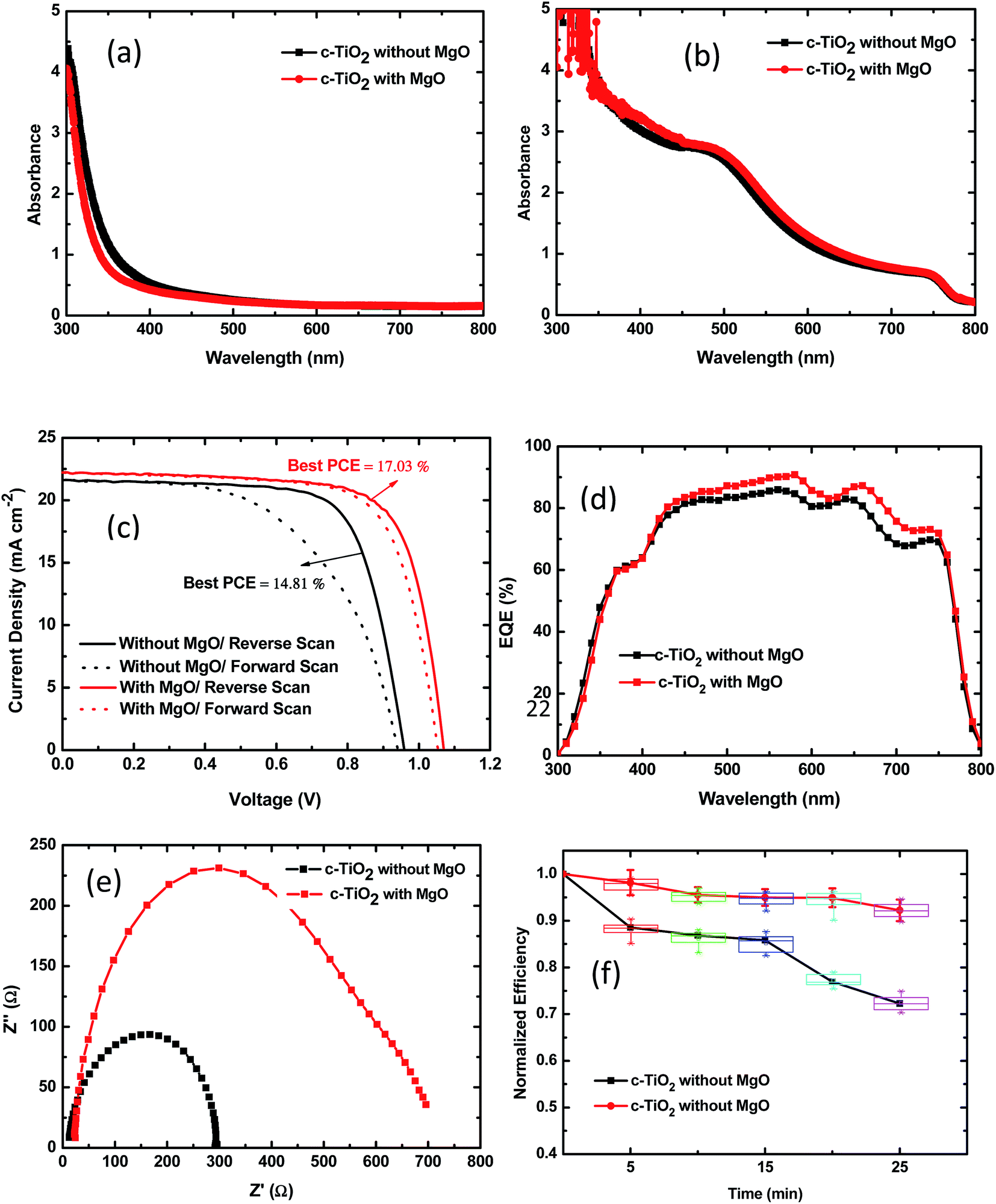 | ||
| Fig. 6 UV-vis spectra of (a) bare and (b) CH3NH3PbI3 coated TiO2 nanorod arrays prepared at 0.04 M TBT with and without MgO modification. (c) J–V characteristics with forward and reverse scans. (d) EQE and (e) EIS (under dark conditions) spectra of the best-performing PSC devices based on c-TiO2 without and with MgO modification. (f) Normalized PCE decay of unsealed devices upon UV irradiation. | ||
Fig. 6(c) shows the J–V curves of the best-performing perovskite solar cells based on c-TiO2 without and with MgO modification at 0.04 M TBT for forward and reverse scans. The corresponding best and mean PV parameters including JSC, VOC, FF and PCE are summarized for the reverse scans in Table 3. As can be seen from Table 3, the PSC device based on c-TiO2 without MgO modification shows an average PCE of 13.38% ± 1.43% resulting from a VOC of 0.96 V ± 0.04 V, JSC of 21.58 ± 0.80 mA cm−2 and FF of 0.67 ± 0.04. In contrast, the PSC with MgO modification has a higher average PCE of 16.24% ± 0.79%, with a VOC of 1.04 V ± 0.02 V, JSC of 21.75 ± 0.40 mA cm−2, and FF of 0.73 ± 0.02. With MgO modification, there are obvious enhancements in the VOC and FF. Besides, there was also a slight enhancement in the JSC, as expected, from the SEM and optical absorption examination and analysis in the previous sections. The improved photocurrent is also supported by the EQE spectra shown in Fig. 6(d). The improved open-circuit voltage can be attributed to the up-shift of the conduction band edge of TiO2 with the MgO coating.42 Moreover, the series resistance (RS) derived from the J–V curves has an impact on the FF.38 The lower RS of the PSC with MgO modification induced its higher FF. As result, the PSC with MgO modified c-TiO2 achieved a champion PCE of 17.03%.
| Device | Device | VOC (V) | JSC (mA cm−2) | Fill factor | PCE (%) | RS (Ω) |
|---|---|---|---|---|---|---|
| Without MgO | Best | 0.96 | 21.63 | 0.71 | 14.81 | 57 |
| Average | 0.96 ± 0.04 | 21.58 ± 0.80 | 0.67 ± 0.04 | 13.38 ± 1.43 | 55 ± 8 | |
| With MgO | Best | 1.06 | 22.01 | 0.73 | 17.03 | 39 |
| Average | 1.04 ± 0.02 | 21.75 ± 0.40 | 0.73 ± 0.02 | 16.24 ± 0.79 | 37 ± 6 |
Mesoscopic CH3NH3PbI3 perovskite hybrid solar cells usually have significant J–V hysteresis with respect to the forward and reverse scan directions owing to charge accumulation or dielectric polarization by ferroelectric properties.43 From Fig. 6(c), the PSC device based on c-TiO2 with MgO modification exhibited not only better device efficiency but also smaller J–V hysteresis with respect to the scan direction than the PSC devices without MgO modification. With MgO modification, the reduced J–V hysteresis can be attributed to the decreased recombination by eliminating the undesirable recombination pathway between TiO2 and the spiro-OMeTAD hole conductor and the reduction in electronic trap states, which enable faster electron transport by the formation of high-quality CH3NH3PbI3 absorbers.44
Fig. 6(e) shows the EIS results for perovskite solar cells based on c-TiO2 without and with MgO modification tested in the dark. In dark conditions, the structure of the PSC device could be simplified as a leaking capacitor.14 From Fig. 6(e), the size of the semicircle is related to the recombination resistance at the interface of the TiO2/perovskite layer and TiO2/hole transport layer. The bigger the diameter of the semicircle, the lower the electron recombination at the interface. The obtained EIS indicates that the recombination resistance increased by several times after MgO modification, which led to a significant decrease in current loss through recombination and an increase in FF.
The stability of perovskite solar cells is a major issue restricting their terrestrial application.14,45 We investigated the stability of unsealed PSCs based on c-TiO2 with and without modification with under UV irradiation. The PSCs were exposed to 365 nm UV illumination at an intensity of 90 mW cm−2, and were removed at certain time intervals to measure the J–V curves under simulated AM1.5 100 mW cm−2 irradiance. In Fig. 6(f), it can be observed that device based on 1D TiO2 NR arrays grown on MgO coated c-TiO2 exhibits a significantly improved stability. Its PCE retains more than 92% of its initial value, even after 25 min UV irradiation in air.
4. Conclusions
We have demonstrated a low-temperature synthesis approach for good ultrathin passivation on TiO2 seeds and high-quality 1D TiO2 nanorod arrays using MgO coating and hydrothermal techniques, respectively. Ultrathin MgO coated c-TiO2 has been used as seeds to hydrothermally grow one-dimensional TiO2 NR arrays for PSCs. Tetrabutyl titanate (TBT) was employed as the Ti precursor. The nanorod diameter and length and areal density of the TiO2 NR arrays were adjusted by controlling the concentration of TBT from 0.3 M to 0.7 M. The effects of MgO modification and TiO2 NR array morphology on the pore-filling of perovskite CH3NH3PbI3 as well as charge separation and recombination at the perovskite/titania nanorod interface have been investigated. Our results show that the TBT concentration strongly affects the VOC, JSC and FF of the 1D TiO2 NR based PSC cell. The best perovskite solar cell based on embedded 1D TiO2 NRs was achieved with MgO coating and at 0.4 M TBT, which displays a PCE of 17.03% with JSC = 22.01 mA cm−2, VOC = 1.06 V, and FF = 0.73. MgO modification elevated the average PCE from 13.38% for the PSCs prepared at 0.4 M TBT without MgO coating to 16.24% for the PSCs formed at the same TBT concentration with MgO coating, exhibiting an approximately 18% improvement in PV performance. This improvement is mainly ascribed to the improved open-circuit voltage and fill factor. Furthermore, MgO modification reduced the J–V hysteresis with respect to the scan direction and improved the UV stability of the non-encapsulated solar cells. This study demonstrates that the employment of ultrathin MgO-coated TiO2 as seeds is a promising strategy to hydrothermally grow high-quality 1D TiO2 nanorod arrays for efficient and stable perovskite solar cells.Conflicts of interest
There are no conflicts to declare.Acknowledgements
This work was supported by the National Natural Science Foundation of China (No. 11274119 and 61275038) and the Large Instruments Open Foundation of East China Normal University.References
- J. Wang, X. Jia, J. Zhou, L. Pan, S. Huang and X. Chen, ACS Appl. Mater. Interfaces, 2016, 8, 26098–26104 CAS.
- S. Mathew, A. Yella, P. Gao, R. H. Baker, B. F. E. Curchod, N. A. Astani, I. Tavernelli, U. Rothlisberger, M. K. Nazeeruddin and M. Grätzel, Nat. Chem., 2014, 6, 242–247 CrossRef CAS PubMed.
- J. Shen, R. Cheng, X. H. Chen, Z. Sun and S. M. Huang, ACS Appl. Mater. Interfaces, 2013, 5, 13000–13005 CAS.
- M. Gloeckler, I. Sankin and Z. Zhao, IEEE J. Photovolt., 2013, 3, 1389–1393 CrossRef.
- P. Jackson, D. Hariskos, R. Wuerz, W. Wischmann and M. Powalla, Phys. Status Solidi RRL, 2014, 8, 219–222 CrossRef CAS.
- J. Shi, Z. Li, D. Zhang, Q. Liu, Z. Sun and S. Huang, Prog. Photovoltaics, 2011, 19, 160–164 CAS.
- M. A. Green, K. Emery, Y. Hishikawa, W. Warta, E. D. Dunlop, D. H. Levi and A. W. Y. Ho-Baillie, Prog. Photovoltaics, 2017, 25, 565–572 Search PubMed.
- M. Afzaal, H. M. Yates, A. Walter, S. Nicolay and C. Ballif, J. Mater. Chem. C, 2017, 5, 4946–4950 RSC.
- W. S. Yang, J. H. Noh, N. J. Jeon, Y. C. Kim, S. Ryu, J. Seo and S. I. Seok, Science, 2015, 348, 1234–1237 CrossRef CAS PubMed.
- M. M. Lee, J. Teuscher, T. Miyasaka, T. N. Murakami and H. J. Snaith, Science, 2012, 338, 643–647 CrossRef CAS PubMed.
- A. Mei, X. Li, L. Liu, Z. Ku, T. Liu, Y. Rong, M. Xu, M. Hu, J. Chen and Y. Yang, Science, 2014, 345, 295–298 CrossRef CAS PubMed.
- C. Zhang, Y. Luo, X. Chen, Y. Chen, Z. Sun and S. Huang, Nano-Micro Lett., 2016, 8, 347–357 CrossRef.
- M. Saliba, T. Matsui, J.-Y. Seo, K. Domanski, J.-P. Correa-Baena, M. K. Nazeeruddin, S. M. Zakeeruddin, W. Tress, A. Abate and A. Hagfeldt, Energy Environ. Sci., 2016, 9, 1989–1997 CAS.
- C. Zhang, Q. Luo, J. Shi, L. Yue, Z. Wang, X. Chen and S. Huang, Nanoscale, 2017, 9, 2852–2864 RSC.
- W. Wu, D. Chen, R. A. Caruso and Y. Cheng, J. Mater. Chem. A, 2017, 5, 10092–10109 CAS.
- E. Hendry, M. Koeberg, B. O'Regan and M. Bonn, Nano Lett., 2006, 6, 755–759 CrossRef CAS PubMed.
- J. Song, S. P. Li, Y. L. Zhao, J. Yuan, Y. Zhu, Y. Fang, L. Zhu, X. Q. Gu and Y. H. Qiang, J. Alloys Compd., 2017, 694, 1232–1238 CrossRef CAS.
- X. Feng, K. Zhu, A. J. Frank, C. A. Grimes and T. E. Mallouk, Angew. Chem., Int. Ed., 2012, 51, 2727–2730 CrossRef CAS PubMed.
- J. Qiu, Y. Qiu, K. Yan, M. Zhong, C. Mu, H. Yan and S. Yang, Nanoscale, 2013, 5, 3245–3248 RSC.
- H. S. Kim, J. W. Lee, N. Yantara, P. P. Boix, S. A. Kulkarni, S. Mhaisalkar, M. Grätzel and N. Park, Nano Lett., 2013, 13, 2412–2417 CrossRef CAS PubMed.
- K. Mahmood, B. S. Swain, A. R. Kirmani and A. Amassian, J. Mater. Chem. A, 2015, 3, 9051–9057 CAS.
- K. Mahmood, B. S. Swain and A. Amassian, Adv. Energy Mater., 2015, 5, 1500568 CrossRef.
- Z. Gu, F. Chen, X. Zhang, Y. Liu, C. Fan, G. Wu, H. Li and H. Chen, Sol. Energy Mater. Sol. Cells, 2015, 140, 396–404 CrossRef CAS.
- Q. Jiang, X. Sheng, Y. Li, X. Feng and T. Xu, Chem. Commun., 2014, 50, 14720–14723 RSC.
- S. S. Mali, C. S. Shim, H. K. Park, J. Heo, P. S. Patil and C. K. Hong, Chem. Mater., 2015, 27, 1541–1551 CrossRef CAS.
- X. Li, S.-M. Dai, P. Zhu, L.-L. Deng, S.-Y. Xie, Q. Cui, H. Chen, N. Wang and H. Lin, ACS Appl. Mater. Interfaces, 2016, 8, 21358–21365 CAS.
- B. Liu and E. Aydil, J. Am. Chem. Soc., 2009, 131, 3985–3990 CrossRef CAS PubMed.
- M. M. Lee, J. Teushcer, T. Miyasaka, T. N. Murakami and H. J. Snaith, Science, 2012, 338, 643–647 CrossRef CAS PubMed.
- Y. Luo, X. Chen, C. X. Zhang, J. J. Li, J. H. Shi, Z. Sun, Z. Wang and S. Huang, RSC Adv., 2015, 5, 56037–56044 RSC.
- X. Jia, Z. Jiang, X. Chen, J. Zhou, L. Pan, F. Zhu, Z. Sun and S. Huang, ACS Appl. Mater. Interfaces, 2016, 8, 3792–3799 CAS.
- A. Kumar, A. Madaria and C. Zhou, J. Phys. Chem. C, 2010, 114, 7787–7792 CAS.
- J. Cai, J. Ye, S. Chen, X. Zhao, D. Zhang, S. Chen, Y. Ma, S. Jin and L. Qi, Energy Environ. Sci., 2012, 5, 7575–7581 CAS.
- Y. Zhou, A. Vasiliev, W. Wu, M. Yang, S. Pang, Z. Kai and N. Padture, J. Phys. Chem. Lett., 2015, 6, 2292–2297 CrossRef CAS PubMed.
- P. Docampo, J. Ball, M. Darwich, G. Eperon and H. Snaith, Nat. Commun., 2013, 4, 2761–2767 Search PubMed.
- A. Baldan, J. Mater. Sci., 2002, 37, 2171–2202 CrossRef CAS.
- J. Jung, K. Zhou, H. Um, Z. Guo, S. W. Jee, K. Park and J. Lee, Opt. Lett., 2011, 36, 2677–2679 CrossRef CAS PubMed.
- K. Bouzidi, M. Chegaar and A. Bouhemadou, Sol. Energy Mater. Sol. Cells, 2007, 91, 1647–1651 CrossRef CAS.
- J. H. Heo, S. H. Im, J. H. Noh, T. N. Mandal, C. S. Lim, J. A. Chang, Y. H. Lee, H. J. Kim, A. Sarkar and M. K. Nazeeruddin, Nat. Photonics, 2013, 7, 486–491 CrossRef CAS.
- X. Li, M. I. Dar, C. Yi, J. Luo, M. Tschumi, S. Zakeeruddin, M. Nazeeruddin, H. Han and M. Grätzel, Nat. Chem., 2015, 7, 703–711 CrossRef CAS PubMed.
- C. Zhang, Y. Luo, X. Chen, W. Ou-Yang, Y. Chen, Z. Sun and S. Huang, Appl. Surf. Sci., 2016, 388, 82–88 CrossRef CAS.
- A. Kulkarni, A. Jena, H. Chen and T. Miyasaka, Sol. Energy, 2016, 136, 379–384 CrossRef CAS.
- J. Wang, M. Qin, H. Tao, W. Ke, Z. Zhao, J. Wan, P. Qin, L. Xiong, H. Lei, H. Yu and G. Fang, Appl. Phys. Lett., 2015, 106, 121104 CrossRef.
- H.-S. Kim, I. Mora-Sero, V. Gonzalez-Pedro, F. Fabregat-Santiago, E. J. Juarez-Perez, N.-G. Park and J. Bisquert, Nat. Commun., 2013, 4, 2242 Search PubMed.
- F. Giordano, A. Abate, J. P. Correa Baena, M. Saliba, T. Matsui, S. H. Im, S. M. Zakeeruddin, M. K. Nazeeruddin, A. Hagfeldt and M. Graetzel, Nat. Commun., 2016, 7, 10379 CrossRef CAS PubMed.
- W. Li, W. Zhang, S. Van Reenen, R. J. Sutton, J. Fan, A. A. Haghighirad, M. B. Johnston, L. Wang and H. J. Snaith, Energy Environ. Sci., 2016, 9, 490–498 CAS.
| This journal is © The Royal Society of Chemistry 2017 |