
 Open Access Article
 This Open Access Article is licensed under a
 Creative Commons Attribution 3.0 Unported Licence
Revealing anisotropy and thickness dependence of Raman spectra for SnS flakes†
Mingling Lia,
Yiming Wu a,
Taishen Lia,
Yulin Chena,
Huaiyi Dinga,
Yue Lina,
Nan Panabc and
Xiaoping Wang*abc
a,
Taishen Lia,
Yulin Chena,
Huaiyi Dinga,
Yue Lina,
Nan Panabc and
Xiaoping Wang*abc
aHefei National Laboratory for Physical Sciences at the Microscale, Department of Physics, University of Science and Technology of China, Hefei, Anhui 230026, P. R. China. E-mail: xpwang@ustc.edu.cn
bSynergetic Innovation Center of Quantum Information & Quantum Physics, University of Science and Technology of China, Hefei, Anhui 230026, P. R. China
cKey Laboratory of Strongly-Coupled Quantum Matter Physics, Chinese Academy of Sciences, School of Physical Sciences, University of Science and Technology of China, Hefei, Anhui 230026, P. R. China
First published on 17th October 2017
Abstract
In this work, we have successfully synthesized SnS flakes with different thicknesses and systematically investigated their polarization-dependent Raman properties. It is found that the different Raman mode of SnS shows distinctly anisotropic thickness dependence. For B3g mode, the polar plot of Raman intensities is insensitive to the flake thickness. However, the behavior of Ag mode is entirely different. Under parallel polarization configuration, with decreasing the flake thickness, the maximum Raman intensity of Ag mode changes from the armchair direction to the zigzag direction with 514.5 nm excitation. The results can be understood by the complex Raman tensor owing to the large absorption of SnS. Moreover, under the perpendicular polarization configuration, the Raman intensity of Ag mode along 45° direction becomes apparently different from that along 135° direction. Our finding not only deepens the understanding of anisotropic Raman properties of SnS but also provides inspiration for further studies on the other 2D IV–VI materials.
Introduction
SnS is an important member of the IV–VI two dimensional materials belonging to the space group D162h.1–3 Like other 2D materials, the in-plane S and Sn atoms are connected by covalent bonds, while the out-plane layers are connected by van der Waals interaction.1,4 However, the existed electron lone pairs (i.e. Sn2+ 5s2) can enhance the interlayer interaction and make it become a distorted NaCl type structure.5 SnS is also an earth-abundant,6 stable7 and non-toxic8 material. Its large absorption coefficient (∼105 cm−1),9,10 as well as the predicted high carrier mobility,7 renders it a great of potential applications in optoelectronic and electronic devices.2,4,11–18 Moreover, similar to the black phosphorous (BP) with puckered honey-comb crystal structure, SnS also possesses anisotropic electronic,19,20 thermoelectric,21–23 piezoelectric24 and optical25,26 properties. Given the strongly anisotropic properties of SnS, the SnS–SnSxSe1−x core–shell heterostructure with anisotropic photoresponse and the SnS-based photodetector with highly anisotropic performance of near-infrared have been achieved.27,28 Additionally, the anisotropic photoresponse properties of SnS can be significantly improved by combining with the plasmon enhancement provided by various metallic nanoparticles.28–30 The anisotropic Raman property of SnS has also been observed and interpreted by Raman tensor theory.25 Like BP,31,32 the behavior can further be used to in situ identify the crystalline orientation to perform the anisotropic electrical and thermoelectrical measurement.20,25 However, similar to that observed in BP,33–38 the strong absorption of SnS would inevitably lead to complex elements in the Raman tensor and therefore change the anisotropic Raman properties with the thickness. However, the dependence of anisotropic behavior of SnS on the thickness has been overlooked. In this regard, it is interesting and imperative to investigate the anisotropic Raman properties of SnS flakes as well as its thickness dependence. However, to the best of our knowledge, there is no systematically study so far about this content, especially in-depth study on the complex Raman tensor elements.In this work, we have successfully synthesized SnS flakes with different thicknesses by physical vapor deposition (PVD) method. We then systematically investigated the polarization-dependent Raman properties of SnS flakes through angle-resolved polarized Raman spectroscopy (ARPRS). It is found that the different Raman modes of SnS show distinctly anisotropic dependence on the thickness of flake. Specially, for B3g mode, the polar plots of Raman intensities for both parallel and perpendicular polarization configurations are insensitive to the flake thickness. On the contrary, the behavior of Ag mode is entirely different. For the parallel polarization configuration, with decreasing the flake thickness, the maximum of Raman intensity changes from the armchair direction to the zigzag direction under 514.5 nm excitation. The result can be interpreted by introducing complex Raman tensor caused by the large absorption.33–36,38 Furthermore, the Raman intensity along 45° direction becomes different from that along 135° direction under the perpendicular polarization configuration. Our finding enriches the understanding of fundamental anisotropic Raman properties of SnS and implies the necessity to consider the thickness of SnS flake to identify its crystalline orientation through Raman characterization.
Experiments
Synthesis of 2D SnS flakes
The SnS flakes with different thicknesses were synthesized by physical vapor deposition (PVD) method.25 The SnS powders (∼0.1 g Alfa Aesar 99.5%) placed in the quartz tube were put onto the center of a horizontal furnace, and the freshly cleaved mica substrates were placed at 15–21 cm downstream. The furnace was evacuated to about 8 mTorr and was then purged with ultrapure Ar. The temperature of the furnace center is set at 630–650 °C. The pressure and the Ar flow were kept at ∼29 Torr and 60 sccm during the growth, respectively. The SnS vapor was carried by Ar flow and deposited onto the substrates, and the SnS flakes were formed subsequently. The growth was maintained for 5–15 min. Then the furnace was cooled down immediately by opening the furnace.Transfer method
The SnS flakes were transferred from mica to SiO2/Si substrate by a water ultrasonic method. The flakes on mica were spin-coated with PMMA (A4 495) at 3000 rpm for 45 s, and then were put onto a hot plate and kept at 120 °C for 3 min. The PMMA film were separated from the mica substrate through dipping it into water and by ultrasonic for several minutes. After that, PMMA containing flakes was transferred onto SiO2/Si substrate and gently dried with lamp heating. Finally, PMMA was removed by dipping in ethyl acetate and acetone, respectively.TEM characterization
TEM, HRTEM images and SAED patterns were collected by a FEI Talos transmission electron microscope operated at 200 kV. The samples for characterization were transferred onto copper grids by the same method described above.Raman measurement
The Raman spectra were obtained by LabRAM HR 800 Raman system under 514.5 nm and 632.8 nm excitation, respectively. The intensities on the samples for both 514.5 nm and 632.8 nm laser in our experiment are controlled at about 0.5 mW (0.4 mW) without (with) a polarizer in the exciting light path. We used 100× objective lens (N.A. = 0.9) and 600 lines per mm grating to collect Raman signals. The spectrum resolutions for 514.5 nm and 632.8 nm excitation are 1.88 cm−1 and 1.21 cm−1, respectively. In polarization-dependent Raman measurement, a polarizer was placed in the incident light path to improve the polarization of exciting light and weaken the depolarization effects caused by objective lens. The direction of polarizer is fixed and the direction of analyzer is alterable. Two configurations of parallel (∥) and perpendicular (⊥) polarization were adopted in the measurement, in which the polarization direction of the polarizer and the analyzer were kept parallel or perpendicular to each other, respectively. The polarization direction of exciting laser with respect to the sample was changed by rotating a custom sample stage by every 5/10/15 degrees. The position and spot area of excitation were cautiously kept the same for each measurement.Results and discussion
Fig. 1a shows the optical image of a typical result of as-grown SnS flakes. As seen, all flakes have square-like morphologies and their averaged size can reach as large as 10 μm, which can be observed more clearly in Fig. 1b. Atomic force microscopy (AFM) (Seiko Instrument Industry Co.) characterization demonstrates that the flake has a smooth surface morphology and its thickness can be down to 7.6 nm, as seen in Fig. 1c. The bright particles on the flake surface are the residues from the transfer process (see Fig. S1 in ESI†). We also note that the morphology of 7.6 nm SnS flake shows rounded corners, while most of flakes shown in Fig. 1a demonstrate sharp corners. Considering that the perfect rhombus structure with sharp corners is the thermodynamic equilibrium state of SnS flake20 and the growth time for the thin flakes is much short (<5 min), we think that there might be no enough time to reach the thermodynamic equilibrium for the thin flakes, resulting in their rounded corners morphology. Additionally, we found that it is difficult to obtain the very thin flakes, because SnS has a relatively strong interlayer interaction5,39 and the complicated phases of S and Sn compounds.40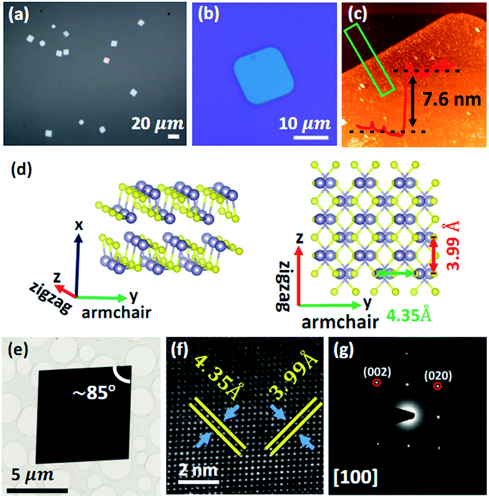 | ||
| Fig. 1 (a) Optical image of as-grown SnS flakes on mica substrate and (b) a thin SnS flake transferred onto SiO2/Si substrate. (c) AFM image of 7.6 nm thick SnS flake. (d) Schematic of crystal structure of SnS from side view (left) and top view (right). (e) TEM image of a SnS flake with a corner angle of ∼85°. (f) HRTEM image and (g) SAED pattern of SnS flake. | ||
We carried out transmission electron microscopy (TEM) as well as the selected area electron diffraction (SAED) characterizations to investigate the structure of the SnS flake and evaluate its crystal quality. Fig. 1d depicts the schematic of crystal structure of SnS. Similar to BP, SnS has also a puckered honeycomb structure, and the two in-plane principle axes are corresponding to armchair direction (y axis) and zigzag direction (z axis), respectively. As seen in Fig. 1e, the SnS flake transferred onto the TEM grids shows a rhombus shape, and the corner angle is estimated to ∼85°, which is in good agreement with previous reports.20,25 Additionally, the perfect 2D rhombus lattice can be found in the high resolution TEM image taken from the flake (Fig. 1f). Two lattice spacings corresponding to the (010) and (001) planes are obtained to be about 4.35 Å and 3.99 Å, respectively. The values are well consistent with the previous results.20,25,41 Fig. 1g demonstrates the corresponding SAED pattern along [100] zone axis of the flake, and the well-defined diffraction spots reveal the good crystalline of as-grown SnS flake. It has been pointed out that the crystalline direction of the SnS can be readily identified from the rhombus shape, i.e., the longer (shorter) diagonal direction is corresponding to the armchair (zigzag) direction.20,25 Therefore, the method is used to ascertain the armchair (or zigzag) direction of the flake for the anisotropic characterization of Raman spectroscopy in the following paragraphs.
The flakes were characterized by the Raman spectroscopy with 514.5 nm laser and the spectra of flakes with different thicknesses are shown in Fig. 2a. As seen, for the thick flakes (169.0 nm and 229 nm), six peaks located at 40.2 cm−1, 49.1 cm−1, 95.9 cm−1, 164.0 cm−1, 192.0 cm−1 and 219.5 cm−1 can be observed clearly. (The Raman peak positions are obtained from fitting the spectrum and its uncertainty is about 0.3 cm−1). These peaks can be attributed to the different Raman modes of Ag and B3g of SnS, respectively,41 as shown in the schematic of Fig. 2b. Specifically, the low frequency Ag (40.2 cm−1) and high frequency Ag (219.5 cm−1) are corresponding to the layer shear mode and the “NaCl” type vibration, respectively. Two other Ag peaks (95.9 cm−1, 192.0 cm−1) are originated from the “waving” and the “breathing” modes, while B3g (49.1 cm−1) and B3g (164.0 cm−1) can be attributed to the shear vibration and the “NaCl” type vibration along zigzag direction, respectively.41 From Fig. 2a, a little red shift of Raman peaks can be observed with decreasing the flake thickness. Taking 7.6 nm thick SnS as an example, the positions of three strong peaks are located at about 93.9 cm−1 (A1g), 151.7 cm−1 (B3g) and 183.2 cm−1 (A2g), respectively. Compared to the results of 229 nm flake, the red shifts can be estimated about 2.0 cm−1 (A1g mode), 12.3 cm−1 (B3g mode) and 8.8 cm−1 (A2g mode), respectively. The phenomenon might be ascribed to the change of bond angle in the thin flake, leading to the smaller of the restoring force for the vibration and the red shift of the corresponding Raman peak.7
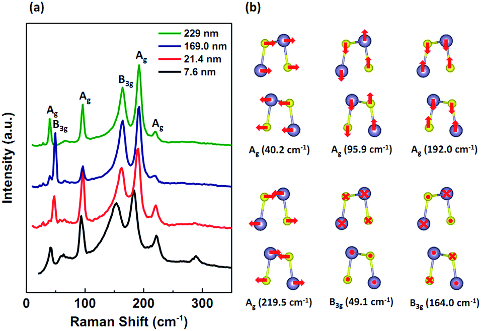 | ||
| Fig. 2 (a) Raman spectra of SnS flakes with different thicknesses under 514.5 nm laser excitation. (b) Vibration diagrams for Ag modes and B3g modes. | ||
To further investigate the anisotropic Raman response of SnS, the polarization-dependent Raman spectroscopy was performed on the SnS flake. As seen in Fig. 3a, the Raman spectrum was collected through the back-scattering configuration with a polarizer and an analyzer placed in the incident and the scattering light paths, respectively. Two configurations of parallel (∥) and perpendicular (⊥) polarization were adopted in the measurement, in which the polarization direction of the polarizer and the analyzer were kept parallel or perpendicular to each other, respectively (Fig. 3a). The polarization angle, defined as the angle between the polarization direction of incident light and the armchair direction of SnS flake, can be tuned from 0° to 360° through rotating a custom sample stage.
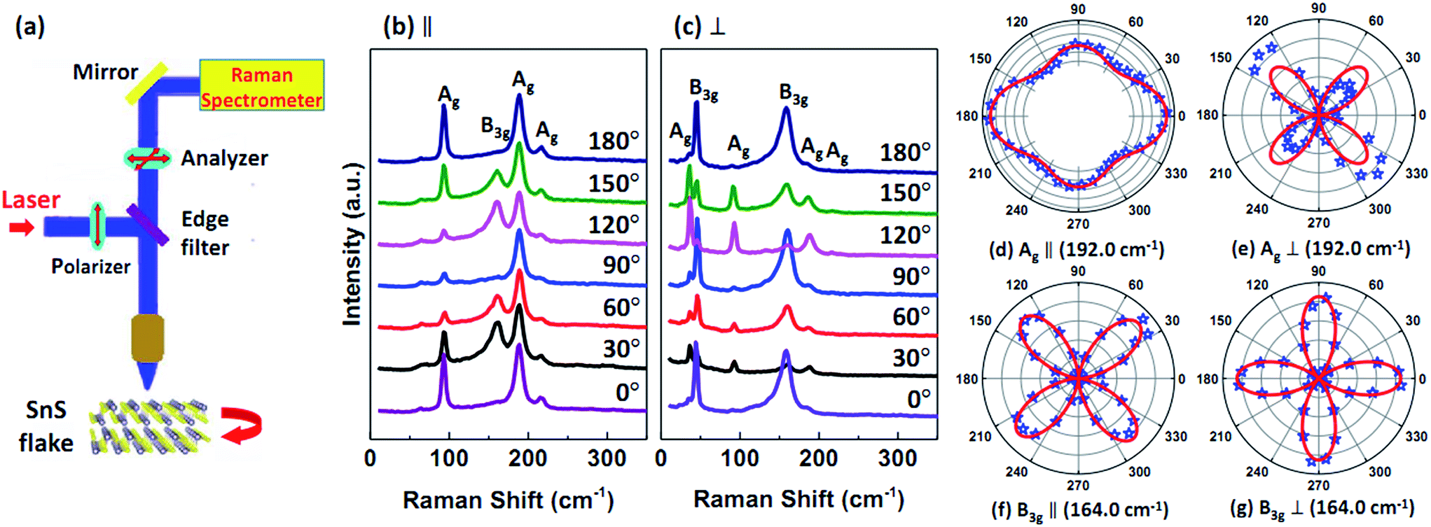 | ||
| Fig. 3 (a) Schematic diagram of Raman measurement for SnS flake. Polarization-dependent Raman spectra of 229 nm thick flake with 514.5 nm laser excitation under (b) parallel and (c) perpendicular polarization configurations. (d–g) The polar plots of intensity of Ag (192 cm−1) and B3g (164.0 cm−1) under parallel and perpendicular polarization, respectively. | ||
Fig. 3b and c demonstrate the anisotropic Raman response of 229 nm SnS flake to the different polarization angles with 514.5 nm excitation under parallel and perpendicular polarization configurations, respectively. As shown in Fig. 3b, Ag (95.9 cm−1), B3g (164.0 cm−1) and Ag (192.0 cm−1) are three strong peaks among the Raman spectra, we therefore concentrate on these three peaks in the following investigation. It can be seen from Fig. 3b and c that the peak intensities of Ag and B3g change periodically with the polarization angle, indicating the anisotropic Raman signals of the SnS flake. The behavior can be observed more clearly with the polar plots for the modes of Ag (192.0 cm−1) and B3g (164.0 cm−1), as shown in Fig. 3d–g. As seen in Fig. 3d, the Raman intensity of Ag (192.0 cm−1, ∥) along armchair is larger than that along zigzag direction. However, it is worth noting that the intensity of zigzag direction is the secondary maximum here, rather than the minimum as the previous works reported.20,25 This implies that the complex Raman tensor should be considered to interpret the result as that treated for BP.33–36,38 On the other hand, as for the modes of B3g (164.0 cm−1, ∥), the intensities along armchair direction and zigzag direction are smallest while the intensities along 45° (225°) and 135° (315°) are the largest (Fig. 3f).
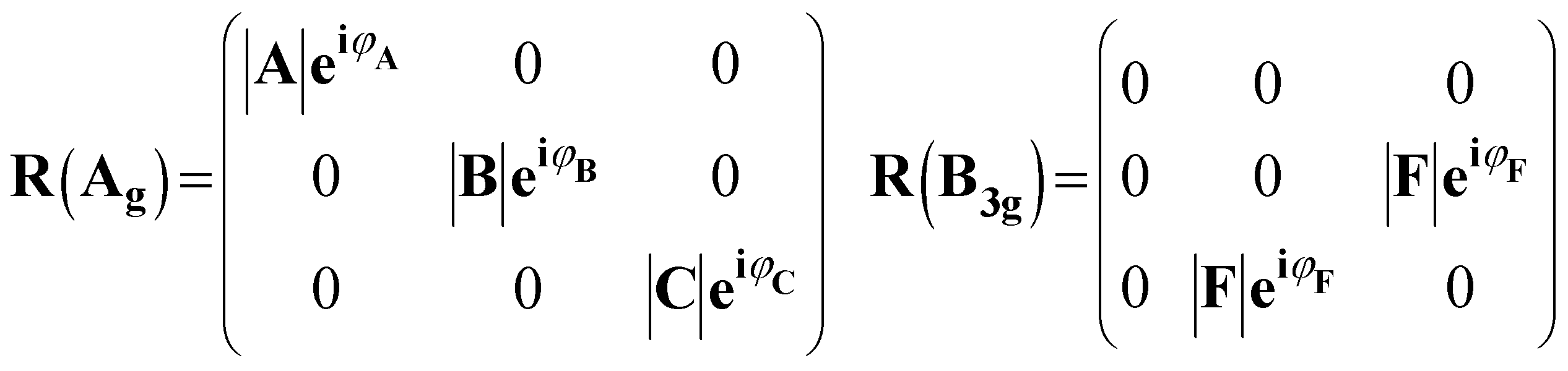
Theoretically, the Raman intensity can be calculated by I ∝ |ei·R·es|2 and the anisotropic behavior is ascribed to the Raman tensor R, which is determined by the detailed crystal structure of material. Owing to its large absorption coefficient,9,10 the Raman tensor elements of the SnS should be complex. Consequently, similar to the treatment for BP,33–36,38 the Raman tensors for Ag and B3g of SnS can be described by
For the polarization angle of θ, the incident light vector is ei = (0, cos![[thin space (1/6-em)]](https://www.rsc.org/images/entities/char_2009.gif) θ, sinθ), while the scattering light vector is es = (0, cosθ, sinθ) for parallel polarization but es = (0, −sinθ, cosθ) for the perpendicular case. Hence, the anisotropic Raman intensities for different modes can be expressed as:
θ, sinθ), while the scattering light vector is es = (0, cosθ, sinθ) for parallel polarization but es = (0, −sinθ, cosθ) for the perpendicular case. Hence, the anisotropic Raman intensities for different modes can be expressed as:
|
I(Ag,∥) ∝ |B|2cos4θ + |C|2sin4θ + 2|B||C|cos2θsin2θcosφCB
| (1) |
|
I(B3g,∥) ∝ |F|2sin22θ
| (2) |
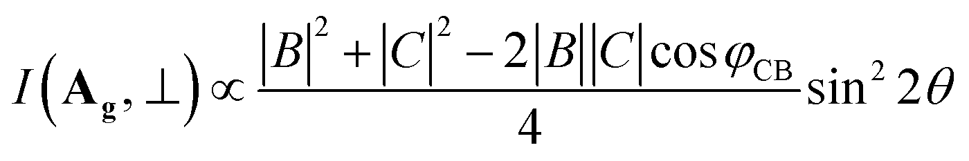 | (3) |
|
I(B3g,⊥) ∝ |F|2cos22θ
| (4) |
We fitted the experiment data with above equations, and the results are plotted in Fig. 3d–g with red solid lines. As seen, the fitting is well consistent with the experiment results. Moreover, combined with the theory and experiment setup, the anisotropic behavior of Ag (192.0 cm−1) mode can be understood from the fact that its vibration motion has more component in armchair direction than that in zigzag direction.33–36,38 As for the mode of B3g (164.0 cm−1), there only exist off-diagonally non-zero elements in the Raman tensor. Therefore, when the polarization of incident light is along armchair (zigzag) direction, the polarization of Raman scattering light will switch to zigzag (armchair) direction. This leads to the intensities of B3g (164.0 cm−1) along armchair and zigzag directions become zero under the parallel polarization configuration (Fig. 3f) but achieve the maximum under the perpendicular polarization configuration, as shown in Fig. 3g.
In order to know whether the anisotropic Raman properties are dependent on the flake thickness, we carried out polarization-dependent Raman measurements on the SnS flakes with different thicknesses. Fig. 4a and b show the results for B3g (164.0 cm−1) under parallel and perpendicular polarization configurations, respectively. As seen, for both configurations, the polar plots of Raman intensity for different thick SnS flakes are similar to those shown in Fig. 3f and g, indicating that the B3g mode is insensitive to the flake thickness. Similar results with 632.8 nm excitation are presented in Fig. S2.† The behavior can be easily understood by the description of eqn (2) and (4). However, as compared to B3g mode, the situation of Ag mode is distinctly different. As seen in the Fig. 4c for the mode of Ag (192.0 cm−1, ∥), the Raman intensity along the armchair direction is larger than that along the zigzag direction for the thick flakes, but the behavior reverses for the thin flake, i.e., the Raman intensity along the zigzag direction becomes larger. This unusual result indicates that the anisotropic Raman response of SnS is strongly dependent on the flake thickness.
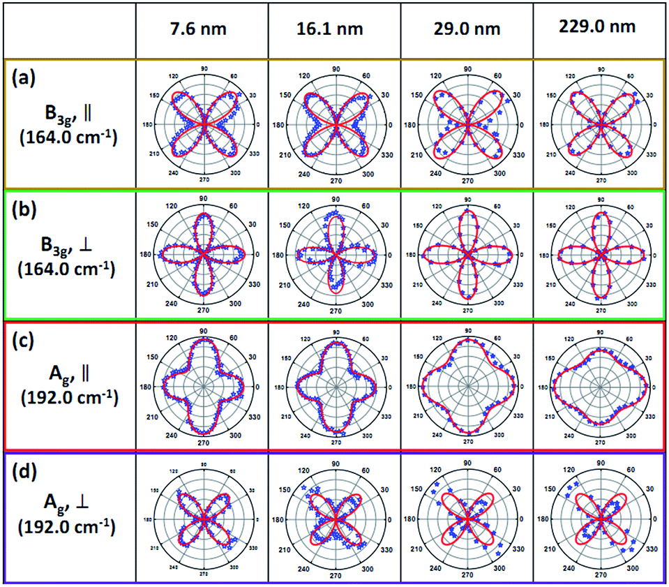 | ||
| Fig. 4 Polar plots of Raman intensities of B3g (164.0 cm−1) and Ag (192.0 cm−1) for different thick SnS flakes with 514.5 nm laser excitation under parallel and perpendicular polarization configurations, respectively. The red curves are fitting results. | ||
As indicated in the aforementioned paragraph, the intensity of Ag mode under parallel polarization configuration can be described by eqn (1), from which we can find that the polar plot of Raman intensity is determined by three parameters, |C|, |B| and φCB. Several calculated results based on eqn (1) are shown in Fig. S3.† Obviously, |C|2/|B|2 is equal to the intensity ratio of the zigzag direction to the armchair direction, reflecting the Raman anisotropy in the y–z plane, while φCB determines the concave degree of the intensity pattern along nearby 45° (or 225°) and 135° (or 315°). Compared to the calculated pattern shown in Fig. S3,† the result in Fig. 4c therefore demonstrates that the ratio of |C|2/|B|2 varies with the thickness of SnS flake. The finding is important because it suggests that it is impossible to identify the armchair direction of SnS flake only through the maximum of Raman intensity, as that used previously.20,25 Moreover, this variation tendency that the Raman intensity along zigzag direction increases with decreasing the flake thickness can also be observed with 632.8 nm excitation (Fig. S4d†).
We used eqn (1) to fit the results of Fig. 4c and S4d,† and the fitting parameters |C|/|B| and φCB are summarized in Fig. 5 and S5,† respectively. As seen in Fig. 5, two features can be found clearly. Firstly, for both 514.5 nm and 632.8 nm excitations, the value of |C|/|B| decreases quickly with increasing the flake thickness and then reaches steady value for fairly thick flakes. The variation of φCB on the flake thickness has similar tendency (Fig. S5†). According to the semi-classical Raman theory, Raman tensor elements |B|eiφB and |C|eiφC are the partial derivatives of the dielectric constant of SnS with respect to the normal coordinates of the corresponding phonon modes along yy and zz directions, respectively.33,38,42 In this context, we consider that the variation of |C|/|B| with the flake thickness is probably attributed to the change of dielectric property for thin SnS flake as compared to that of the bulk. More importantly, Fig. 5 demonstrates |C| > |B| for thin SnS flakes under 514.5 nm excitation, which is distinctly unusual as compared to the previous reports.20,25 We ascribe the underlying reason to the strongly resonant absorption in zigzag direction for thin flake,43 leading to the change of the dielectric dispersion relationship and hence the Raman tensor. More investigation is surely needed to elucidate this conjecture in the future work. Secondly, the values of |C|/|B| with 514.5 nm excitation are larger than those with 632.8 nm excitation for all different thick flakes. The behavior can be further observed clearly by comparing Fig. 4c and S4d.† Because |C|/|B| = 1 is the indicative of Raman isotropy along armchair and zigzag directions, the result in Fig. 5 suggests that the anisotropic Raman spectrum can be observed more readily with 632.8 nm excitation.
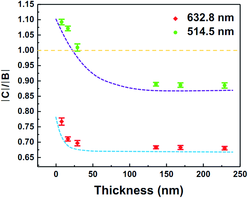 | ||
| Fig. 5 Variation of |C|/|B| with the thickness of SnS flake for Ag mode (192.0 cm−1) with 514.5 nm and 632.8 nm laser excitation, respectively. The lines are guides for eye. | ||
Finally, we return to the anisotropic properties of Ag (192.0 cm−1, ⊥) of SnS flakes with different thicknesses. As seen in Fig. 4d, all polar plots show the maximum values of Raman intensities along 45° (or 225°) and 135° (or 315°), while the minimum intensities are along armchair and zigzag directions. This is ascribed to that all non-diagonal elements in the Raman tensor of Ag modes are zero. As a consequence, when the polarization of excitation light is along armchair or zigzag direction, the final intensity of Raman scattering will become zero under perpendicular polarization configuration. Also from the prediction of eqn (2), the Raman intensity along 45° (or 225°) direction must be equal to that along 135° (or 315°) for Ag (⊥) mode. However, this contrasts obviously to the experimental observation for Ag mode (192.0 cm−1, ⊥) shown in Fig. 4d, in which the intensity difference between 45° (225°) and 135° (315°) is apparent for the SnS flakes, especially for 29.0 nm and 229 nm flakes. The behavior has also been reported in SnS.25 It is difficult to understand this phenomenon at present due to the fact that the 45° (or 225°) and 135° (or 315°) directions are equal from the viewpoint of crystal structure. One possible reason is attributed to the circular dichroism originated from the uniquely puckered anisotropic structure of SnS, leading to the different absorption along 45° and 135° directions.
Conclusions
We have successfully synthesized SnS flakes with different thicknesses by physical vapor deposition method. The anisotropy and the thickness dependence of Raman properties are systematically investigated through the polarization-dependent Raman spectra. Both B3g and Ag modes can be observed from the SnS flakes but they show distinctly anisotropic thickness dependence. On the one hand, the anisotropy of B3g mode is found to be independent of the flake thickness. On the other hand, the Ag mode shows entirely different behavior. Under parallel polarization configuration and 514.5 nm excitation, the maximum Raman intensity of Ag mode changes from the armchair direction to the zigzag direction with decreasing the flake thickness. The result is interpreted through the complex Raman tensor due to the large absorption of SnS. Under the perpendicular polarization configuration, the Raman intensity of Ag mode along 45° direction becomes different from that along 135° direction. Our finding also implies that the anisotropic electron–phonon interactions in SnS flakes are dependent on the thickness. This work can enrich the understanding of fundamental anisotropic Raman properties of SnS and provide the inspiration for further studies on other 2D anisotropic materials.Conflicts of interest
There are no conflicts of interest to declare.Acknowledgements
We acknowledge the financial supports from MOST of China (2016YFA0200602), National Natural Science Foundation of China (21421063, 11474260, 11374274, 11504364), the Chinese Academy of Sciences (XDB01020200) and Anhui Natural Science Foundation (1608085QA17).Notes and references
- J. R. Brent, D. J. Lewis, T. Lorenz, E. A. Lewis, N. Savjani, S. J. Haigh, G. Seifert, B. Derby and P. O'Brien, J. Am. Chem. Soc., 2015, 137, 12689 CrossRef CAS PubMed.
- V. Steinmann, R. Jaramillo, K. Hartman, R. Chakraborty, R. E. Brandt, J. R. Poindexter, Y. S. Lee, L. Sun, A. Polizzotti, H. H. Park and R. G. Gordon, Adv. Mater., 2014, 26, 7488 CrossRef CAS PubMed.
- L. C. Gomes and A. Carvalho, Phys. Rev. B: Condens. Matter Mater. Phys., 2015, 92, 085406 CrossRef.
- M. Patel, A. Chavda, I. Mukhopadhyay, J. Kim and A. Ray, Nanoscale, 2016, 8, 2293 RSC.
- D. I. Bletskan, M. M. Bletskan and K. E. Glukhov, J. Solid State Chem., 2017, 245, 34 CrossRef CAS.
- P. Sinsermsuksakul, K. Hartman, S. B. Kim, J. Heo, L. Sun, H. H. Park, R. Chakraborty, T. Buonassisi and R. G. Gordon, Appl. Phys. Lett., 2013, 102, 053901 CrossRef.
- C. Xin, J. X. Zheng, Y. T. Su, S. K. Li, B. K. Zhang, Y. C. Feng and F. Pan, J. Phys. Chem. C, 2016, 120, 22663 CAS.
- K. T. R. Reddy, N. K. Reddy and R. W. Miles, Sol. Energy Mater. Sol. Cells, 2006, 90, 3041 CrossRef.
- R. Eymard and A. Otto, Phys. Rev. B: Solid State, 1977, 16, 1616 CrossRef CAS.
- L. Makinistian and E. A. Albanesi, Phys. Status Solidi B, 2009, 246, 183 CrossRef CAS.
- B. Ghosh, M. Das, P. Banerjee and S. Das, Semicond. Sci. Technol., 2009, 24, 025024 CrossRef.
- K. T. Ramakrishna Reddy, N. Koteswara Reddy and R. W. Miles, Sol. Energy Mater. Sol. Cells, 2006, 90, 3041 CrossRef CAS.
- C. Xia, J. Du, W. Xiong, Y. Jia, Z. Wei and J. Li, J. Mater. Chem. A, 2017, 5, 13400 CAS.
- M. Patel, H. S. Kim and J. Kim, Nanoscale, 2017 10.1039/c7nr03370b.
- M. Ristov, G. Sinadinovski, M. Mitreski and M. Ristova, Sol. Energy Mater. Sol. Cells, 2001, 69, 17 CrossRef CAS.
- X. Zhou, L. Gan, Q. Zhang, X. Xiong, H. Li, Z. Zhong, J. Han and T. Zhai, J. Mater. Chem. C, 2016, 4, 2111 RSC.
- T. Rath, L. Gury, I. Sanchez-Molina, L. Martinez and S. A. Haque, Chem. Commun., 2015, 51, 10198 RSC.
- F. Lu, J. Yang, R. Li, N. Huo, Y. Li, Z. Wei and J. Li, J. Mater. Chem. C, 2015, 3, 1397 RSC.
- S. Sucharitakul, U. R. Kumar, R. Sankar, F. C. Chou, Y. T. Chen, C. H. Wang, C. He, R. He and X. P. A. Gao, Nanoscale, 2016, 8, 19050 RSC.
- Z. Tian, C. L. Guo, M. X. Zhao, R. R. Li and J. M. Xue, ACS Nano, 2017, 11, 2219 CrossRef CAS PubMed.
- R. Guo, X. Wang, Y. Kuang and B. Huang, Phys. Rev. B: Condens. Matter Mater. Phys., 2015, 92, 115202 CrossRef.
- Asfandiyar, T. R. Wei, Z. Li, F. H. Sun, Y. Pan, C. F. Wu, M. U. Farooq, H. Tang, F. Li, B. Li and J. F. Li, Sci. Rep., 2017, 7, 43262 CrossRef CAS PubMed.
- L. Medrano Sandonas, D. Teich, R. Gutierrez, T. Lorenz, A. Pecchia, G. Seifert and G. Cuniberti, J. Phys. Chem. C, 2016, 120, 18841 CAS.
- R. Fei, W. Li, J. Li and L. Yang, Appl. Phys. Lett., 2015, 107, 173104 CrossRef.
- J. Xia, X. Z. Li, X. Huang, N. N. Mao, D. D. Zhu, L. Wang, H. Xu and X. M. Meng, Nanoscale, 2016, 8, 2063 RSC.
- R. E. Banai, L. A. Burton, S. G. Choi, F. Hofherr, T. Sorgenfrei, A. Walsh, B. To, A. Cröll and J. R. S. Brownson, J. Appl. Phys., 2014, 116, 013511 CrossRef.
- J. Xia, D. Zhu, X. Li, L. Wang, L. Tian, J. Li, J. Wang, X. Huang and X.-M. Meng, Adv. Funct. Mater., 2016, 26, 4673 CrossRef CAS.
- Z. Zhang, J. Yang, K. Zhang, S. Chen, F. Mei and G. Shen, J. Mater. Chem. C, 2017 10.1039/c7tc02865b.
- C. J. Murphy, T. K. Sau, A. M. Gole, C. J. Orendorff, J. Gao, L. Gou, S. E. Hunyadi and T. Li, J. Phys. Chem. B, 2005, 109, 13857 CrossRef CAS PubMed.
- S. D. Hudson and G. Chumanov, J. Phys. Chem. C, 2008, 112, 19866 CAS.
- J. Wu, N. Mao, L. Xie, H. Xu and J. Zhang, Angew. Chem,. Int. Ed., 2015, 54, 2366 CrossRef CAS PubMed.
- X. Wang, A. M. Jones, K. L. Seyler, V. Tran, Y. Jia, H. Zhao, H. Wang, L. Yang, X. Xu and F. Xia, Nat. Nanotechnol., 2015, 10, 517 CrossRef CAS PubMed.
- H. B. Ribeiro, M. A. Pimenta, C. J. S. de Matos, R. L. Moreira, A. S. Rodin, J. D. Zapata, E. A. T. de Souza and A. H. C. Neto, ACS Nano, 2015, 9, 4270 CrossRef CAS PubMed.
- J. Kim, J. U. Lee, J. Lee, H. J. Park, Z. Lee, C. Lee and H. Cheong, Nanoscale, 2015, 7, 18708 RSC.
- X. Ling, S. Huang, E. H. Hasdeo, L. Liang, W. M. Parkin, Y. Tatsumi, A. R. Nugraha, A. A. Puretzky, P. M. Das, B. G. Sumpter, D. B. Geohegan, J. Kong, R. Saito, M. Drndic, V. Meunier and M. S. Dresselhaus, Nano Lett., 2016, 16, 2260 CrossRef CAS PubMed.
- A.-L. Phaneuf-L'Heureux, A. Favron, J.-F. Germain, P. Lavoie, P. Desjardins, R. Leonelli, R. Martel and S. Francoeur, Nano Lett., 2016, 16, 7761 CrossRef PubMed.
- W. Lu, X. Ma, Z. Fei, J. Zhou, Z. Zhang, C. Jin and Z. Zhang, Appl. Phys. Lett., 2015, 107, 021906 CrossRef.
- W. Luo, Q. Song, G. Zhou, D. Tuschel and G. Xia, arXiv, 1610.03382, 2016.
- P. M. NikoliC, L. j. Iljkovic, P. Mihajlovic and B. LavrenEic, J. Phys. C: Solid State Phys., 1977, 10, L289 CrossRef CAS.
- R. C. Sharma and Y. A. Chang, J. Phase Equilib., 1986, 7, 269 CAS.
- H. R. Chandrasekhar, R. G. Humphreys, U. Zwick and M. Cardona, Phys. Rev. B: Solid State, 1977, 15, 2177 CrossRef CAS.
- A. C. Albrecht, J. Chem. Phys., 1961, 34, 1476 CrossRef CAS.
- G. A. Tritsaris, B. D. Malone and E. Kaxiras, J. Appl. Phys., 2013, 113, 233507 CrossRef.
Footnote |
| † Electronic supplementary information (ESI) available: AFM image of 13.2 nm SnS flake, polar plots of B3g (164.0 cm−1) and Ag (95.9 cm−1 and 192.0 cm−1) with different thickness, the calculated polar plots of Ag (∥) mode with different |C|/|B| and φCB, and variation of φCB with the thickness of SnS flake for Ag mode (192.0 cm−1). See DOI: 10.1039/c7ra09430b |
| This journal is © The Royal Society of Chemistry 2017 |