
 Open Access Article
 This Open Access Article is licensed under a
 Creative Commons Attribution 3.0 Unported Licence
Graphene growth controlled by the position and number of layers (n = 0, 1, and more than 2) using Ni and MgO patterned ultra-flat Cu foil†
Aram Lee‡
a,
Kyoung Soon Choi‡ b,
Jinheon Parka,
Tae Soo Kima,
Jouhahn Leeb,
Jae-Young Choi*c and
Hak Ki Yu*a
b,
Jinheon Parka,
Tae Soo Kima,
Jouhahn Leeb,
Jae-Young Choi*c and
Hak Ki Yu*a
aDepartment of Energy Systems Research, Department of Materials Science and Engineering, Ajou University, Suwon, 16499, Korea. E-mail: hakkiyu@ajou.ac.kr; jy.choi@skku.edu
bThe Advanced Nano Surface Research group, Korea Basic Science Institute, Daejeon 34133, Korea
cSchool of Advanced Institute of Nanotechnology (SAINT), School of Advanced Materials Science & Engineering, Sungkyunkwan University, Suwon, 16419, Korea
First published on 10th November 2017
Abstract
The catalytic activity of transition metals with regard to carbo-hydroxyl molecules (CxHy) has triggered new technological developments in graphene growth. Both the opening of the Dirac-point by controlling the number of graphene layers as well as the patterning of the graphene are critical for applications such as transistor-based electronics. In this work, we have developed a method to control the position and number of layers (n = 0, 1, and more than 2) during graphene growth based on our previous key ideas. This was achieved by using pre-patterned (Ni pre-patterned for more than 2 layers due to its high carbon solubility compared to Cu and MgO pre-patterned for 0 layer graphene due to the low catalytic activity and carbon solubility) ultra-flat Cu foils made using the peeled off method from a c-plane sapphire substrate.
Introduction
Graphene, a single layer of graphite, has recently attracted a lot of attention due to its remarkable material properties and possible applications in many emerging areas such as graphene-based electronic devices.1 Since the charge carriers in graphene behave like massless Dirac fermions, graphene shows ballistic charge transport, which makes it an ideal material for circuit fabrication.2,3 However, graphene lacks a bandgap around the Fermi level, which is essential in semiconductor transistors and for conductivity control by electronic valves.4 Several theories and experimental results have proven that there are ways to open up the band-gap at the Dirac point, such as synthesis of graphene nano-ribbons (GNR), gas-molecule adsorption (with gases like hydrogen), and electrical tuning of multilayer graphene.5–11 Manufacturing GNRs is a bottom-up method, which is a huge barrier for mass-scale device fabrication.5 Gas-molecule absorption is quite unstable and there are difficulties in controlling the adsorption and desorption. As a result, the electrical tuning of multi-layer (n >= 2) graphene is one of the easiest ways to open the Dirac point.In order to make an electrical circuit using graphene, the patterning of graphene is also important. Photo-lithography based patterning followed by oxygen plasma etching is the most conventional method to make graphene patterns.12,13 However, this process requires several steps and there is a possibility for defects to be induced during the energetic plasma collision. Recently, J. M. Tour et al. showed that sputtering zinc on graphene and dissolving the latter with dilute acid (such as HCl) can remove only the top layer of graphene which was in contact with the sputtered zinc film.14 By using this method, they could control the number of layers of graphene after transferring the CVD-grown graphene several times followed by partial etching with photo-lithography and zinc sputtering. However, the structure of the multiple stacked CVD-graphene by using conventional polymer supporting layers is not an ideal Bernal AB stacking.15 Moreover, this could result in a polymer residue between the graphene layers.16 Hence, a direct graphene growth method with the ability to control the position and the number of layers without any additional process would be ideal for real world applications.
Graphene can be grown on various catalytic metal surfaces since several metals have interstitial carbon solubility at high temperatures.17 If we have hetero-structured metal surfaces with different carbon solubility, we can directly synthesize the required number of graphene layers on them (multiple layers of graphene on the metal surface which has high carbon solubility, a monolayer of graphene on the metal surface which has low carbon solubility, and no graphene layer on the non-catalytic surface with low carbon solubility). We have focused on the pattering of Ni and MgO hetero-catalyst on a Cu surface. Ni has a lattice structure and atomic size similar to Cu. However, it has a higher carbon solubility compared to Cu (0.001–0.008 weight% at 1084 °C for Cu, 0.6 weight% for Ni at 1326 °C), resulting in a relatively large number of graphene layers when compared to Cu.18,19 The MgO surface, which has a strong tendency to chemically bond with water molecules present in the ambient conditions by forming Mg(OH)2, has a low catalytic activity with carbo-hydroxyl molecules as well as low carbon solubility.20 As a result, the MgO patterned area on Cu can be expected to have no layers of graphene. In addition, in order to obtain a flat and high quality n-layer graphene surface, we have used extremely flat hetero-catalytic (Ni patterned Cu foil) metal foils using the peel-off techniques based on our previous key ideas as shown in Fig. 1 (The MgO layer is patterned after peeling-off Ni patterned Cu foil to avoid mechanical cracking of ceramic materials).21 By using this approach, we can control not only the number of graphene layers just after the CVD growth process, without any additional steps, but also the position of n-graphene by Ni and MgO pattering using a conventional photolithography technique.
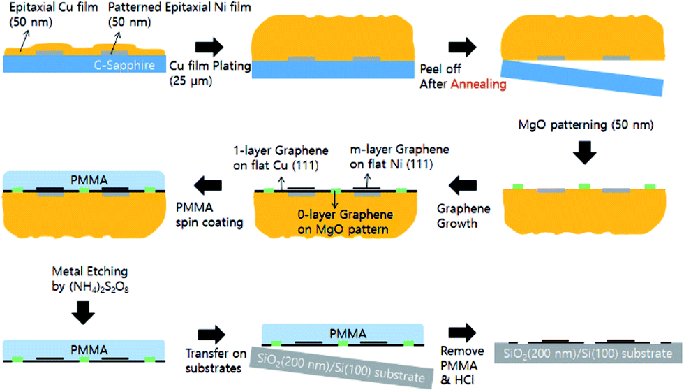 | ||
| Fig. 1 Schematic of the fabrication procedure for peeled-off Cu foil with Ni patterning and additional MgO patterning for n-layer (n = 0, 1, and more than 2) graphene growth. The synthesized graphene can be transferred to the target substrate SiO2 (200 nm)/Si (100). | ||
Experimental section
Preparation of Ni patterned peeled-off Cu catalyst & MgO patterning
C-Plane sapphire (Double side polished, Crystal Bank Research Institute, Pusan National University, Korea) was used as a mother substrate. After cleaning sequentially with acetone, isopropyl alcohol, and de-ionized water, 500 μm × 500 μm patterns were made by photo-lithography. The sapphire substrate was dipped in HCl + DI water (volume ratio 1![[thin space (1/6-em)]](https://www.rsc.org/images/entities/char_2009.gif) :1) for 1–2 min to remove surface contamination right before metal deposition. Ni films of 50 nm thickness were deposited by electron beam deposition using a high purity Ni source. After making the Ni pattern by removing the photo-resist in acetone, a Cu film of 50 nm thickness was deposited on the entire sample by electron beam deposition using a high purity Cu source. The Cu and Ni films were grown at a rate of 0.03 nm s−1. The growth chamber pressure was maintained at about 10−6 Torr during deposition and the substrate was held at room temperature.
:1) for 1–2 min to remove surface contamination right before metal deposition. Ni films of 50 nm thickness were deposited by electron beam deposition using a high purity Ni source. After making the Ni pattern by removing the photo-resist in acetone, a Cu film of 50 nm thickness was deposited on the entire sample by electron beam deposition using a high purity Cu source. The Cu and Ni films were grown at a rate of 0.03 nm s−1. The growth chamber pressure was maintained at about 10−6 Torr during deposition and the substrate was held at room temperature.
For plating Cu on the epitaxial Ni patterned- Cu film, the cathode (Ni patterned Cu film on C-plane sapphire) and anode (Bulk Cu stick) were electrically connected to a Keithley 2400 digital source meter to maintain constant current density (15 mA cm−2). During electroplating, the voltage between the electrodes varied between 0.2 and 0.3 V, the growth rate was about 16 μm h−1 and controlled to yield a final thickness of ∼25 μm. The temperature of the electroplating solution was 60 °C. Due to large compressive stresses between the thick Cu foil and the C-plane sapphire substrate, the Cu foils (Ni patterned) could be peeled-off from the sapphire substrate.
To fabricate the non-catalytic MgO surface on the peeled-off Cu surface, 100 μm × 100 μm patterns were made by photo-lithography. The MgO films with 200 nm film thickness were also grown by electron beam evaporation using MgO pellet sources (2 mm diameter with 0.5 mm thickness, 99.995%, Mitsubishi Materials Co.) at about 10−6 Torr during deposition at room temperature.
Graphene growth and transfer
Ni patterned peeled-off Cu foils with additional MgO patterns were loaded into a quartz tube reaction chamber. The growth process proceeded in the following manner: first, the pressure in the growth chamber was pumped down to 3 mTorr using a mechanical pump. Second, a 40 sccm flow of hydrogen gas was introduced into the chamber at 950 mTorr. Third, the Cu foils were heated to 950 °C over 60 min. Lastly, 6 sccm of methane gas with 20 sccm of hydrogen was introduced into the chamber for 10 min with the total pressure maintained at 460 mTorr during the graphene synthesis. After the growth process was complete, the furnace was cooled down rapidly to room temperature under 20 sccm of hydrogen.To transfer the graphene layer, first, one side of the graphene/Cu foils was spin coated with polymethyl methacrylate (PMMA) on a spin coater at 2000 rpm for 60 s and dried in ambient conditions for 1 h. Then, the uncoated side of the graphene samples, i.e. the side that is polymer free, was etched in an oxygen plasma for 30 s at 100 W to remove the carbon present on this side. After the Cu foils and the Nickel patterns (with the exception of the MgO pattern) were totally etched away in 0.3 M (NH4)2S2O8 solution for 12 h, the floating graphene/PMMA films were washed several times with DI water. The resulting graphene/PMMA films were transferred onto a target substrate and dried at ambient conditions for 24 h before being heat treated at 180 °C for 30 min in order to increase the adhesion between the graphene and target substrate (SiO2 covered Si substrate). Finally, the PMMA layers were removed by sequential washing with acetone, isopropyl alcohol, and de-ionized water.
Analysis
The X-ray diffraction spectra were measured by a powder X-ray diffractometer (Mac Science, M18XHF22, 18 kW) using monochromated Cu Kα radiation and a scintillation detector. The Raman spectra were obtained with a LabRAM HR 800 (HORIBA Yvon GmbH) spectrometer under the following conditions: excitation wavelength of the He–Ne laser: 633 nm, spot size of the laser beam: 5 μm in diameter, measurement time: 20 s. Surface investigations were performed with a scanning electron microscope (SEM, Leo 1525). The optical microscope (OM) images were taken with a U-MSSP49 OLYMPUS microscope. X-ray photoemission spectroscopy (XPS) was carried out in an AXIS Ultra DLD model (KRATOS, U.K.) at the Korea Basic Science Institute. XPS spectra were obtained at a base pressure of 2.0 × 10⁻¹⁰ Torr at 300 K with a monochromatic Al Kα line at 1486.69 eV. The I–V characteristic measurements were done using a HP4156 semiconductor parameter analyzer.Results and discussion
To make a Ni-patterned, peeled-off Cu foil, the adhesion between the epitaxial Ni and Cu film is very important. As shown in Fig. 2a, some part of the epitaxial Ni pattern can remain on the C-sapphire although the metallic bonding between Cu and Ni is quite strong. For the improved transfer of the epitaxial Ni pattern to the Cu-foil, the surface atom diffusion between Cu and Ni is essential by providing thermal energy, resulting in strong bonding by diffusion similar to Au–Sn systems. When the sample was heated at 600 °C for 1 min the transfer was clear, but the diffusion was too strong to get a clean Ni interface (Fig. 2b). For the ideal diffusion bonding, both the activation energy for vacancy formation and diffusion energy should be considered.22 These variables have an Arrhenius type relation with temperature and hence we have to optimize the annealing temperature before the peeling-off process. Fig. 2c shows the optical microscope images of the peeled-off Ni-patterned Cu foil (annealed in vacuum before peeling from the sapphire substrate). Heating causes the transfer ratio to dramatically increase and the optimum (complete transfer without remaining residual on the sapphire surface) condition was found to be annealing at 500 °C for 1 min. For a better understanding of the Ni–Cu interfacial structure, we had measured X-ray diffraction using a powder diffractometer before the peeling-off process (Fig. 2d). Up to 500 °C, there is no significant change in the diffraction profile (we can only see Ni (111) and Cu (111) with Al2O3 (0006)). However, at 600 °C, we can see the broadness of the diffraction peak between Cu (111) and Ni (111), due to formation of a Cu–Ni substitutional alloy. Based on the Hume-Rothery rule, the Cu and Ni can form a perfect substitutional alloy without a secondary compound phase.23 This means that we can increase the adhesion between Ni and Cu until 500 °C by forming the Cu–Ni intermixing alloy only at the interface. However, if we increase the temperature higher than 600 °C, the intermixing can happen in the entire area of the Ni–Cu film resulting in damage of the clean Ni surface as shown in Fig. 2b.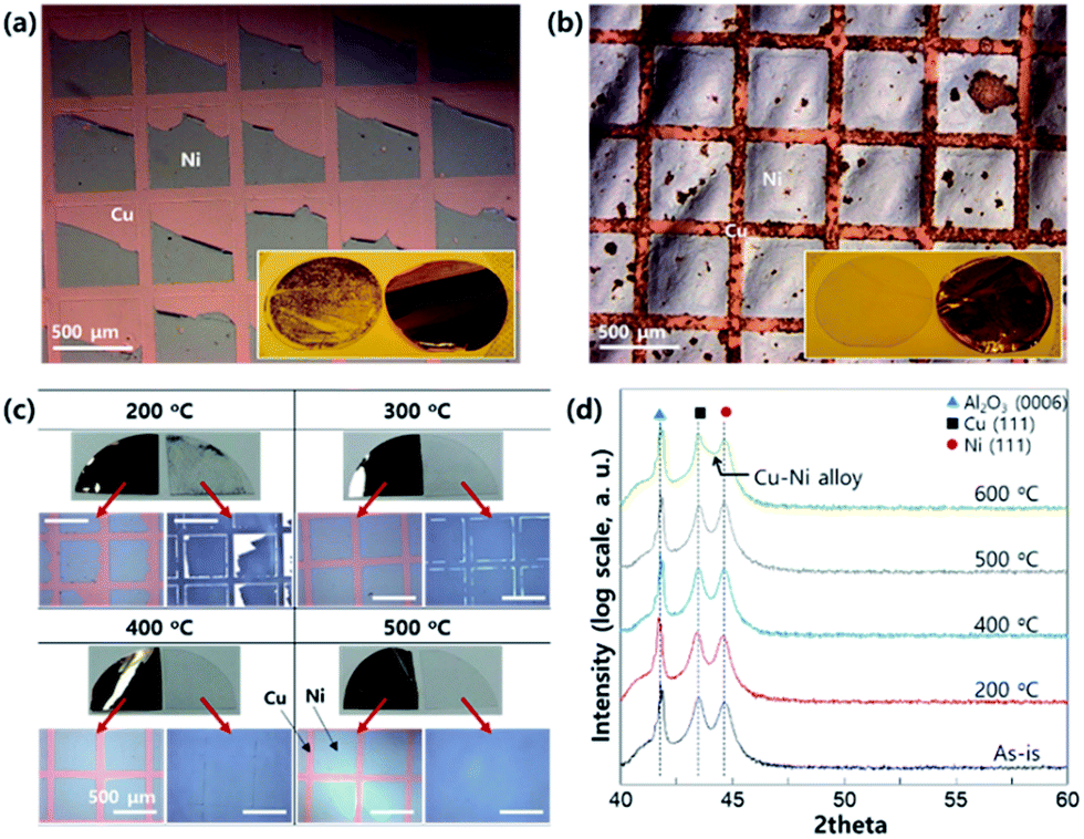 | ||
| Fig. 2 OM images and digital camera images (insets) of Ni-patterned Cu foil after the peeling-off process; (a) direct peeling off after Cu plating (b) after annealing at 600 °C for 1 min before peeling-off (under vacuum). (c) Digital camera images of a quarter 2-inch wafer and OM images of the sapphire side and the Ni-patterned Cu foil after peeling off. (d) XRD patterns of c-sapphire/Ni (50 nm)/Cu (50 nm) film at different annealing temperatures (1 min under vacuum) without Cu plating. | ||
Because the refractory oxide material MgO has very high melting point about 2852 °C, it is difficult to have alloy reaction with Ni and Cu near 1000 °C. Thus, we focused on the Ni–Cu alloy system in detail. To control the number of layers of graphene on the Ni-patterned, peeled-off Cu foil, several CVD runs were carried out by changing the growth temperature as shown in the Fig. S1a.† There is no significant difference between the Ni and Cu areas for the sample grown at 1000 °C (the melting point of Cu is 1084 °C) for 10 min due to strong intermixing between Ni and Cu. When we reduce the growth temperature to 950 °C, there is a clear difference between the Ni and Cu zones as seen in the optical microscope images (graphene was transferred on SiO2/Si surface, Fig. S1b†). Since the monolayer can absorb only 2.3% of incident light, the interference of reflected light between SiO2 and n-graphene (n is number of graphene layers) is different, resulting in a clear color difference seen in the optical microscope.24 However, if the growth temperature is below 900 °C, the solubility of carbon is very low (solubility of carbon depends on the temperature), resulting in isolated growth of graphene (Fig. S1c†). As a result, the optimized temperature for the layer controlled growth between Ni and Cu catalyst is 950 °C.
Fig. 3 shows the optical microscope images and Raman spectra of the transferred graphene. zone 1 and 2 (Fig. 3a) indicate the transferred graphene that were grown on epitaxial Cu and Ni, respectively. Similarly, zone 3 and 4 (Fig. 3b) show the transferred graphene grown on epitaxial Cu and MgO pattern, respectively. The Raman spectra of graphene grown on the Cu area (zone 1 and 3) show typical features associated with monolayer graphene, namely an intense and symmetric 2D line.25 However, the spectrum of graphene grown on patterned Ni (zone 2) shows relatively high G, D intensity compared to the graphene grown on Cu. The G line is related to the amount of carbon, meaning that a significant amount of carbon exists on the Ni patterned area.26 Moreover, the strong D line is related to the destruction of the hexagonal symmetry of the sp2 bonded carbon sheet. Based on the Raman results, we conclude that graphene grown on Ni surfaces tends to have a higher solubility of carbon compared to that grown on Cu surfaces. This results in multi-layer graphene growth on Ni whereas only a monolayer of graphene can grow on the Cu surface. The Raman spectrum of zone 4, where the MgO pattern existed, shows that there are no carbon related materials (i.e. no graphene layer) on that surface due to the non-catalytic behaviour of MgO and the low carbon solubility. The contaminations shown in our experimental results can be originated from the graphene grown on back-side Cu surface (electro-plated surface). Although we did the oxygen plasma etching to remove the graphene, the rough electro-plated Cu surface makes it difficult to have clean plasma etching effect. In addition, we studying to reduce the contamination by polishing the electro-plated Cu surface.
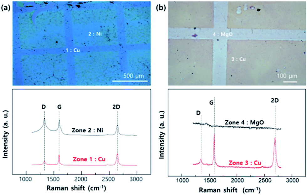 | ||
| Fig. 3 OM images and Raman spectra of layer controlled graphene transferred to SiO2 (200 nm)/Si (100) substrates by (a) Ni pattern on Cu area (b) MgO pattern on Cu area. | ||
The chemical bonding state of carbon on each surface (Cu, Ni, and MgO) was examined by X-ray photoemission study of C 1s core level spectra (Fig. 4). The C 1s core level peak of the graphene surface could be deconvoluted into sp2 C–C binding, sp3 C–C binding, C–O single bonding and C![[double bond, length as m-dash]](https://www.rsc.org/images/entities/char_e001.gif) O double binding such as CO and OC–O–C.27 After the CVD process, the surface contamination peaks such as C–O, CO and O–CO decreased, whereas the sp2/sp3 ratio significantly increased in Cu (from 0.4 to 10.6) and Ni (from 0.2 to 20.2), implying the formation of sp2 bonded graphene on the metal catalysts (Fig. 4a and b). The binding energy shifts to lower energy levels after graphene growth due to the quasi-free-standing nature of graphene (weak bonding) on the metal catalyst, whereas the carbon adsorbates are strongly chemisorbed before the growth process.28–30 On the other hand, the C 1s core level of the MgO surface is significantly different. The ratio of external contamination peaks decreased and only the low intensity sp2 C–C and sp3 C–C bonding existed after the synthesis process. Hence, a strong chemisorption of carbon residuals occurred without the formation of a graphene layer due to non-catalytic activity of MgO.
O double binding such as CO and OC–O–C.27 After the CVD process, the surface contamination peaks such as C–O, CO and O–CO decreased, whereas the sp2/sp3 ratio significantly increased in Cu (from 0.4 to 10.6) and Ni (from 0.2 to 20.2), implying the formation of sp2 bonded graphene on the metal catalysts (Fig. 4a and b). The binding energy shifts to lower energy levels after graphene growth due to the quasi-free-standing nature of graphene (weak bonding) on the metal catalyst, whereas the carbon adsorbates are strongly chemisorbed before the growth process.28–30 On the other hand, the C 1s core level of the MgO surface is significantly different. The ratio of external contamination peaks decreased and only the low intensity sp2 C–C and sp3 C–C bonding existed after the synthesis process. Hence, a strong chemisorption of carbon residuals occurred without the formation of a graphene layer due to non-catalytic activity of MgO.
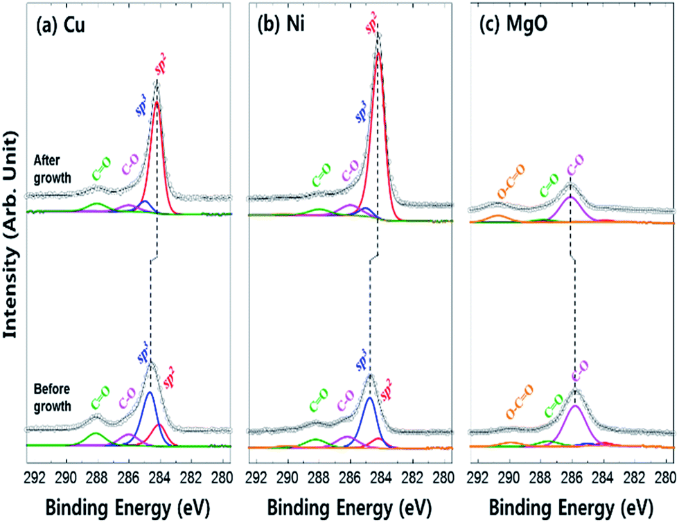 | ||
| Fig. 4 X-ray photoemission spectra of C 1s core level for each surface before and after graphene growth by CVD process (a) Cu, (b) Ni, and (c) MgO. | ||
To check the electrical properties of each n-graphene zone (shown in Fig. 5a and b), several I–V measurements were done as shown in Fig. 5c. When one of the electrodes are in a 0-layer graphene zone (Z), there is no current flow (Z-S1, Z-S2, Z-M). Additionally, when one of the electrodes is in the multi-layer graphene (M), the current flow (S1-M, S2-M) is higher than that of the single layer electrodes (S1 and S2), as per I–V measurements. These results prove that the electrical properties of each n-graphene zone match well with the known properties of graphene.31,32
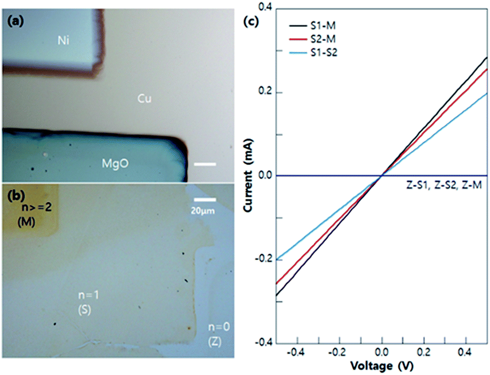 | ||
| Fig. 5 OM image of Ni–MgO patterned Cu foil (a) before graphene growth and (b) after transfer to SiO2/Si substrate (c) I–V characteristics between 0-layer (Z), 1-layer (S1 and S2), and multilayer (M) graphene zones. | ||
Conclusions
In this work, we have successfully controlled the number of graphene layers (n-layer) by using a Cu–Ni–MgO hetero catalyst having a different catalytic activity and carbon solubility. In order to make a flat and high quality graphene surface, we have used extremely flat hetero-catalytic (Ni patterned Cu) metal foils using optimized pre-annealing and peel-off techniques based on our previous key ideas. Graphene on the Ni surface tends to form multi-layers (n >= 2), whereas n = 1 for graphene on the Cu surface and n = 0 on the MgO patterned area. By patterning the Ni and MgO surface using photo-lithography we can control not only the number of graphene layers but also their position. Besides, this idea can reduce the processing sequences, polymer impurities, and fabrication material cost compare to conventional pattering process. We believe that we can improve the quality of n-layer graphene on Ni patterned surface by modulating several growth conditions and this important experiment proves that n-layer graphene can be grown with a hetero Cu–Ni–MgO catalyst.Conflicts of interest
There are no conflicts to declare.Acknowledgements
This research was supported by Basic Science Research Program through the National Research Foundation of Korea (NRF) and funded by the Ministry of Science, ICT & Future Planning (NRF-2016R1C1B1009030)Notes and references
- K. S. Novoselov, A. K. Geim, S. V. Morozov, D. Jiang, Y. Zhang, S. V. Dubonos, I. V. Grigorieva and A. A. Firsov, Science, 2004, 306, 666–669 CrossRef CAS PubMed.
- Y. Zhang, Y.-W. Tan, H. L. Stormer and P. Kim, Nature, 2005, 438, 201–204 CrossRef CAS PubMed.
- K. S. Novoselov, A. K. Geim, S. Morozov, D. Jiang, M. Katsnelson, I. Grigorieva, S. Dubonos and A. Firsov, Nature, 2005, 438, 197–200 CrossRef CAS PubMed.
- F. Xia, D. B. Farmer, Y.-m. Lin and P. Avouris, Nano Lett., 2010, 10, 715–718 CrossRef CAS PubMed.
- X. Li, X. Wang, L. Zhang, S. Lee and H. Dai, Science, 2008, 319, 1229–1232 CrossRef CAS PubMed.
- D. V. Kosynkin, A. L. Higginbotham, A. Sinitskii, J. R. Lomeda, A. Dimiev, B. K. Price and J. M. Tour, Nature, 2009, 458, 872–876 CrossRef CAS PubMed.
- L. Tapasztó, G. Dobrik, P. Lambin and L. P. Biró, Nat. Nanotechnol., 2008, 3, 397–401 CrossRef PubMed.
- R. Balog, B. Jørgensen, L. Nilsson, M. Andersen, E. Rienks, M. Bianchi, M. Fanetti, E. Lægsgaard, A. Baraldi and S. Lizzit, Nat. Mater., 2010, 9, 315–319 CrossRef CAS PubMed.
- D. C. Elias, R. R. Nair, T. Mohiuddin, S. Morozov, P. Blake, M. Halsall, A. Ferrari, D. Boukhvalov, M. Katsnelson and A. Geim, Science, 2009, 323, 610–613 CrossRef CAS PubMed.
- K. F. Mak, C. H. Lui, J. Shan and T. F. Heinz, Phys. Rev. Lett., 2009, 102, 256405 CrossRef PubMed.
- E. V. Castro, K. Novoselov, S. Morozov, N. Peres, J. L. Dos Santos, J. Nilsson, F. Guinea, A. Geim and A. C. Neto, Phys. Rev. Lett., 2007, 99, 216802 CrossRef PubMed.
- K. S. Kim, Y. Zhao, H. Jang, S. Y. Lee, J. M. Kim, K. S. Kim, J.-H. Ahn, P. Kim, J.-Y. Choi and B. H. Hong, Nature, 2009, 457, 706–710 CrossRef CAS PubMed.
- W. Liu, B. L. Jackson, J. Zhu, C.-Q. Miao, C.-H. Chung, Y.-J. Park, K. Sun, J. Woo and Y.-H. Xie, ACS Nano, 2010, 4, 3927–3932 CrossRef CAS PubMed.
- A. Dimiev, D. V. Kosynkin, A. Sinitskii, A. Slesarev, Z. Sun and J. M. Tour, Science, 2011, 331, 1168–1172 CrossRef CAS PubMed.
- H. K. Yu and J.-L. Lee, Sci. Rep., 2014, 4, 6589 CrossRef CAS PubMed.
- M. Gulde, S. Schweda, G. Storeck, M. Maiti, H. K. Yu, A. M. Wodtke, S. Schäfer and C. Ropers, Science, 2014, 345, 200–204 CrossRef CAS PubMed.
- C.-M. Seah, S.-P. Chai and A. R. Mohamed, Carbon, 2014, 70, 1–21 CrossRef CAS.
- R. B. McLellan, Scr. Metall., 1969, 3, 389–391 CrossRef CAS.
- A. Handbook, ASM In., 1992, 9, 2 Search PubMed.
- H. K. Yu, W.-K. Kim, E. C. Park, J. S. Kim, B.-W. Koo, Y.-W. Kim, J. H. Ryu and J.-L. Lee, J. Phys. Chem. C, 2011, 115, 17910–17914 CAS.
- H. K. Yu, K. Balasubramanian, K. Kim, J.-L. Lee, M. Maiti, C. Ropers, J. Krieg, K. Kern and A. M. Wodtke, ACSNnano, 2014, 8, 8636–8643 CAS.
- K. McCarty, J. Nobel and N. Bartelt, Nature, 2001, 412, 622–625 CrossRef CAS PubMed.
- W. Hume-Rothery, J. Inst. Met., 1926, 35, 319–335 Search PubMed.
- R. R. Nair, P. Blake, A. N. Grigorenko, K. S. Novoselov, T. J. Booth, T. Stauber, N. M. Peres and A. K. Geim, Science, 2008, 320, 1308 CrossRef CAS PubMed.
- L. Malard, M. Pimenta, G. Dresselhaus and M. Dresselhaus, Phys. Rep., 2009, 473, 51–87 CrossRef CAS.
- A. Niilisk, J. Kozlova, H. Alles, J. Aarik and V. Sammelselg, Carbon, 2016, 98, 658–665 CrossRef CAS.
- H. K. Yu, J. Electrochem. Soc., 2015, 162, E277–E281 CrossRef CAS.
- J. Díaz, G. Paolicelli, S. Ferrer and F. Comin, Phys. Rev. B, 1996, 54, 8064 CrossRef.
- A. Al Taleb, H. K. Yu, G. Anemone, D. Farías and A. M. Wodtke, Carbon, 2015, 95, 731–737 CrossRef CAS.
- A. Politano, I. Radović, D. Borka, Z. Mišković, H. Yu, D. Farías and G. Chiarello, Carbon, 2017, 114, 70–76 CrossRef CAS.
- Y. Wang, S. W. Tong, X. F. Xu, B. Özyilmaz and K. P. Loh, Adv. Mater., 2011, 23, 1514–1518 CrossRef CAS PubMed.
- P. Willke, C. Möhle, A. Sinterhauf, T. Kotzott, H. K. Yu, A. Wodtke and M. Wenderoth, Carbon, 2016, 102, 470–476 CrossRef CAS.
Footnotes |
| † Electronic supplementary information (ESI) available. See DOI: 10.1039/c7ra09305e |
| ‡ These authors contributed equally to this work. |
| This journal is © The Royal Society of Chemistry 2017 |