
 Open Access Article
 This Open Access Article is licensed under a
 Creative Commons Attribution 3.0 Unported Licence
Development of low temperature stoichiometric solution combustion derived transparent conductive ternary zinc tin co-doped indium oxide electrodes†
Pavan Pujarac,
Srinivas Gandlac,
Mukesh Singhc,
Bikesh Guptaa,
Kartick Tarafderb,
Dipti Guptac,
Yong-Young Noh d and
Saumen Mandal*a
d and
Saumen Mandal*a
aDepartment of Metallurgical and Materials Engineering, National Institute of Technology Karnataka (NITK), Surathkal-575025, India. E-mail: smandal@nitk.edu.in
bDepartment of Physics, National Institute of Technology Karnataka (NITK), Surathkal-575025, India
cPlastic Electronics and Energy Laboratory, Department of Metallurgical Engineering and Materials Science, Indian Institute of Technology Bombay, Powai 400 076, India
dDepartment of Energy & Materials Engineering, Dongguk University, 30, Pildong-ro 1-gil, Jung-gu, Seoul, 04620, Republic of Korea
First published on 13th October 2017
Abstract
Here, the development of transparent conductive zinc tin co-doped indium oxide (IZTO: In1.4Sn0.3Zn0.3O3) ternary electrodes is addressed through low temperature solution combustion processing. Optimization of fuel to oxidizer ratio offers low temperature (∼130 °C) of combustion with balanced redox reaction. The thin films of IZTO annealed at different temperatures showed a decreasing trend in the resistivity with a fixed order of 10−2 Ω cm and the film with a highest Hall mobility of 5.92 cm2 V−1 s−1 resulted at 400 °C. All the films with different temperatures of annealing were smooth (rms ≤ 2.42 nm) in nature and the IZTO film annealed at 200 °C is 83% transparent in the visible spectra. The effective band gap of 0.9 eV determined from first-principles density functional theory gives clear evidence for the conducting nature of IZTO. The thin film transistor fabricated with IZTO as a gate electrode with poly(methyl methacrylate) and pentacene as the dielectric and channel material, respectively, exhibited a saturation mobility of 0.44 cm2 V−1 s−1 and Ion/Ioff ratio of 103. Further, the printability of the IZTO combustible precursor is established which resulted in anti-edge deposition of the printed feature.
1. Introduction
The scientific interest in the field of transparent conducting oxides (TCOs) is increasing continuously because of the co-existence of transparency, conductivity and solution processability offered by these materials in optoelectronic devices; such as electrodes for flat panel displays,1–3 anodes for organic light emitting diodes,4–6 touch panels,7 and solar cells.8,9 Indium based binary (tin doped indium oxide (ITO),10,11 zinc doped indium oxide (IZO)12,13) and ternary (zinc and tin co-doped indium oxide (IZTO)14,15) oxides are a few such widely accepted TCOs. Co-doping gives a larger window of composition and shows conductivity of one order less than ITO;16 this helps in tailoring the properties of IZTO for particular applications. As evidence; the IZTO film can be used as transparent conductor as well as transparent semiconductor. The Gibb's triangle at 1275 °C focused on two solid solutions of IZTO;1 which can be used as a TCO; namely zinc and tin co-doped indium oxide bixbyite: In(2−2x)ZnxSnxO3 where x ≤ 0.4 and indium substituted Zn2SnO4 (zinc stannate spinel): Zn2−xSn1−xIn2xO4 where x = 0–0.45. On the other hand; Zn(9−2x)InxSnxO(9+1.5x) (1 ≤ x ≤ 4) and ZnIn(8−x)SnxO(13+0.5x) (1 ≤ x ≤ 7) are semiconducting in nature.17 In addition to the advantages of IZTO mentioned above, it is cost effective and 60% of indium usage can be reduced11,18,19 compared to ITO. The reason for unusual combination of properties (transparency and conductivity) of doped oxides is extent of doping and crystal structure.1 Indium oxide has two polymorphs namely; (a) a cubic bixbyite type (c-In2O3) with a = 10.116 Å, Z = 16 is stable under atmospheric pressure conditions.20 (b) Corundum type (rh-In2O3)20,21 with a = 5.491 Å, c = 14.526 Å, Z = 6 is metastable under ambient atmospheric conditions;22 which can be stabilized by (i) in quasi 1D nanostructures, (ii) in the sol–gel synthesized In2O3 and (iii) Sn4+/Fe3+/N3− doped In2O3. Further, the optical band gap of oxides varies from 3 to 4 eV, mention a few; ITO: ∼4.0 eV,23 TiO2: 3.2 eV,24 ZnO: 3.36 eV,25 IZTO: 3.0 to 3.5 eV (ref. 8) in the form of thin films; although optical band gap is high, ITO and IZTO exhibit high conductivity.8,23Over the years thin films of TCOs have been grown using different techniques, such as sputtering, pulse laser deposition etc. Although several evaporation techniques are available; but have got limitations as far as cost, production rate, large scale and mass production are concerned; these problems can be addressed by solution processing techniques. There are basically two routes for the solution processed oxide films, namely; the precursor solution containing respective metal cations can be coated using techniques such as spin coating,26,27 dip coating,28,29 spray coating;30 and another route, where oxide nano particles/nano structures (wires etc.) can be dispersed into a solvent and the resulting dispersant can be utilized for the fabrication of thin film using different coating31,32 and printing33 methods. Kim et. al., reported solution processed amorphous IZTO thin film as an active layer in thin film transistors (TFT); nature of the film was confirmed through transmission electron microscopy.17 Here we emphasize on the synthesis of IZTO powders using self-propagating solution combustion technique and spin coated combustible precursors to fabricate IZTO thin films.
The solution combustion technique uses metal precursors along with fuel and oxidizers. Generally nitrates employed as oxidizers and hydrocarbons as fuel. It has been reported that bulk materials such as carbides, borides, silicides, phosphides, hydrides, chalcogenides34 and binary oxides35 can be synthesized via solution combustion technique; here we extend the technique to conductive complex ternary oxides. The unique advantage of the combustion processing is that the stoichiometry of the product can be tailored based on the amount of precursors used. In addition, the process is simple and fast.
In this study, we address solution combustion synthesis of ternary complex oxide system In1.4Zn0.3Sn0.3O3, where acetylacetone (C5H8O2) serves as fuel. In the process, oxidation of cation of nitrates (oxidizer; O) occurs along with the reduction reaction of fuel (F); thus proper selection of F and O becomes crucial. Here we report IZTO synthesized using different fuel to oxidizer ratios (F![[thin space (1/6-em)]](https://www.rsc.org/images/entities/char_2009.gif) :O). A detailed theoretical study with X-ray diffraction helped us to predict the unit cell and band structure of IZTO. Finally, predicted band structure is developed using density functional theory (DFT) which is correlated with the optical band gap from absorption spectroscopy. Also, the IZTO film fabricated further utilized as transparent electrode and a TFT constituting of which is fabricated in order to show applicability of present solution combustion derived IZTO. To address printability of the combustible precursor a line feature is printed and confirmed its anti-edge deposit nature.
:O). A detailed theoretical study with X-ray diffraction helped us to predict the unit cell and band structure of IZTO. Finally, predicted band structure is developed using density functional theory (DFT) which is correlated with the optical band gap from absorption spectroscopy. Also, the IZTO film fabricated further utilized as transparent electrode and a TFT constituting of which is fabricated in order to show applicability of present solution combustion derived IZTO. To address printability of the combustible precursor a line feature is printed and confirmed its anti-edge deposit nature.
2. Experimental section
2.1. Preparation and characterization of combustible precursors
Solution containing 500 mg of indium nitrate (In(NO3)3, Sigma Aldrich), 92.7 mg of tin chloride (SnCl4, Sigma Aldrich) and 67.4 mg zinc nitrate (Zn(NO3)2, Tarson Chemicals, India) in 2-methoxyethanol (2-ME, Tarson Chemicals, India), were prepared. Addition of the fuel – acetylacetone (C5H8O2, Tarson Chemicals, India) was designed based on the balanced chemical equation (eqn (1)). In order to analyze the effect of excess and lean redox mixtures; two more solutions with varying F:O were prepared; quantity of fuel in each case was decided based on the molar ratios of fuel and oxidizer (F:O). An optimum F:O (=0.5; obtained from balanced redox reaction, eqn (1)), fuel rich (F:O = 5) and fuel lean (F:O = 0.05) precursors were obtained by adding 100 μl, 1000 μl and 10 μl of C5H8O2 respectively to solutions containing 18 ml (0.2 M) of 2-ME. All three solutions were stirred for 72 h to make them clear and stable. Precursors (by keeping in vacuum oven at 40 °C for 8 h) were utilized for the thermal analysis (heating rate = 10 °C min−1) using differential scanning calorimetry (DSC, NETZSCH-DSC-404F1) calibrated with pure indium (purity: 99.999%). All three solutions were combusted on a hot plate and product-oxide powder was calcined at 600 °C for 2 h. X-ray diffraction (XRD, JEOL-JPX 8) patterns were traced at a scanning rate of 1° min−1 for both calcined and as-combusted powder. Selected area electron diffraction (SAED) patterns were recorded for as-combusted powder using Transmission Electron Microscope (TEM, JEM-2100, JEOL) operated at 200 kV.| 28In(NO3)3 + 6SnCl4 + 6Zn(NO3)2 + 19C5H8O2 → 2In14Sn3Zn3O30 + 95CO2 + 76H2O + 48N2 + 12Cl2 | (1) |
2.2. Thin film fabrication and characterization
Solution with optimum F:O (= 0.5) is spin coated (2000 rpm, 35 s) on to the glass substrate (Corning 1737F: Sigma Aldrich) and annealed at different temperatures (200 °C, 300 °C and 400 °C) on a hot plate for 30 min; desired thickness is achieved by multi-coating utilizing 50 μl of combustible precursors in each coat. The obtained thin film was characterized using UV visible spectroscopy (SHIMADZU, UV-3600), Atomic Force Microscopy (AFM, Park XE-100), Grazing Incidence Angle X-ray Diffraction (GIAXRD, RIGAKU-Japan) and X-ray photoelectron spectroscopy (XPS, model: PHI5000VersaProbeII). In order to know the carrier concentration (N), Hall mobility (μH) and resistivity (ρ), Hall effect measurements were carried out for all three samples annealed at different temperatures.
2.3. Fabrication and characterization of thin film transistor
In order to reveal the efficacy of the IZTO film to be used as a conducting thin film a TFT with a bottom gate top contact architecture is fabricated on to a glass substrate with spin coated (1000 rpm, 30 s and annealed at 90 °C for 30 min) commercial grade poly(methyl methacrylate) – PMMA (Microchem XR1541) as the dielectric layer followed by thermally deposited 50 nm pentacene as a channel layer. Finally gold contacts (30 nm) were evaporated thermally with a channel length (L) of 100 μm and channel width (W) 1000 μm. The fabricated devices were characterized in ambient atmosphere in dark using semiconductor characterization system having a KEITHLEY-4200 source meter. The saturation mobility (μsat) of the TFT is calculated from eqn (2) and other characteristics such as Ion:Ioff, threshold voltage (VT) were determined from transfer characteristics. In order to measure capacitance, a device having a configuration metal/insulator/metal, was fabricated on commercial ITO coated glass (ITO/PMMA/Au) using broadband dielectric spectrometer.
 | (2) |
2.4. Theoretical study of unit cell and band structure of IZTO
To predict the unit cell of the zinc and tin co-doped In2O3, we have considered cubic In2O3 as the parent structure with space group Ia3 (number 199). Few indium atoms in the In2O3 unit cell were randomly chosen and replaced by tin and zinc atoms. Next we have performed first-principles DFT calculations on each predicted unit cell using Vienna ab initio simulation package36–38 which uses pseudopotentials and the projector augmented wave approach. We used the Perdew–Burke–Ernzerhof generalized gradient approximation for treating the exchange–correlation potential. The onsite Coulomb interaction correction was taken into account by using GGA + U method. A sufficiently high-energy cutoff (500 eV) was used in each calculation to obtain accurate results. In our simulations the forces on each of the atoms were calculated using the Hellmann–Feynman theorem, and were subsequently used to perform a conjugate gradient structural relaxation. The structural optimizations were continued until the forces on the atoms converged to less than 1 meV Å−1. Finally, the total energy of optimized geometries was compared considering the optimized structure with minimum total energy for further electronic band structure investigation.2.5. Inkjet printing of IZTO combustible solution
To show the printability of the combustible IZTO solution, line feature is printed (width ∼270 μm) using inkjet printer (Micro-Fab Technologies Inc.) having a nozzle of 60 μm orifice diameter. Two number of passes were printed subsequently and annealed at 150 °C then slowly rising the annealing temperature to 200 °C and finally the film was annealed at 400 °C for 30 min. The line profile of printed feature is traced by thickness profilometer (Dektak XT; make: Bruker).3. Results and discussion
The stoichiometry (In2−2xZnxSnxO3; x = 0.3) selected in this study was adopted from the Gibb's triangle1 as shown in Fig. 1a; though the maximum solubility is upto 40 at% (x = 0.4, Fig. 1a), in order to avoid secondary non-conducting phases only 30 at% doping has been selected. Further, the schematic (Fig. 1b) guides the reader through both bulk-powder synthesis and thin film fabrication methods employing same combustible precursors. The DSC thermogram of combustible precursors (Fig. 1b) with varying F:O ratios shows endothermic peaks in all three cases at around 125 °C corresponds to solvent evaporation; which is noted to be boiling point of 2-ME. The exothermic response of DSC at 136.4 °C, 129.9 °C and 131.9 °C in case of F:O = 0.05, 0.5 and 5 respectively gives an evidence of combustion reaction. It is clear that the combustion temperature is low in case of balanced redox mixture. This confirms that, minimum temperature is required to initiate the reaction provided there should be an optimum mixture of combustible elements as depicted in the eqn (1); 129.9 °C is the minimum temperature ever reported for combustion of indium based ternary oxides. Kim et. al.35 reported a combustion temperature of 200 °C for acetylacetone based unary system-indium oxide. With fuel lean (F:O = 0.05) and fuel rich (F:O = 5) mixtures the DSC exothermic shows right shift (Fig. 1b) confirming increase in combustion temperature. Commenting on the type of combustion; the combustion of optimum F:O mixture shows clean burning of redox mixture but the fuel rich shows excessive fumes depicting burning of excess fuel. In addition, fuel lean mixture shows sudden flaming (ESI S1†). These variants in burning are due to amounts of fuel and oxidizer present in the redox mixture.39
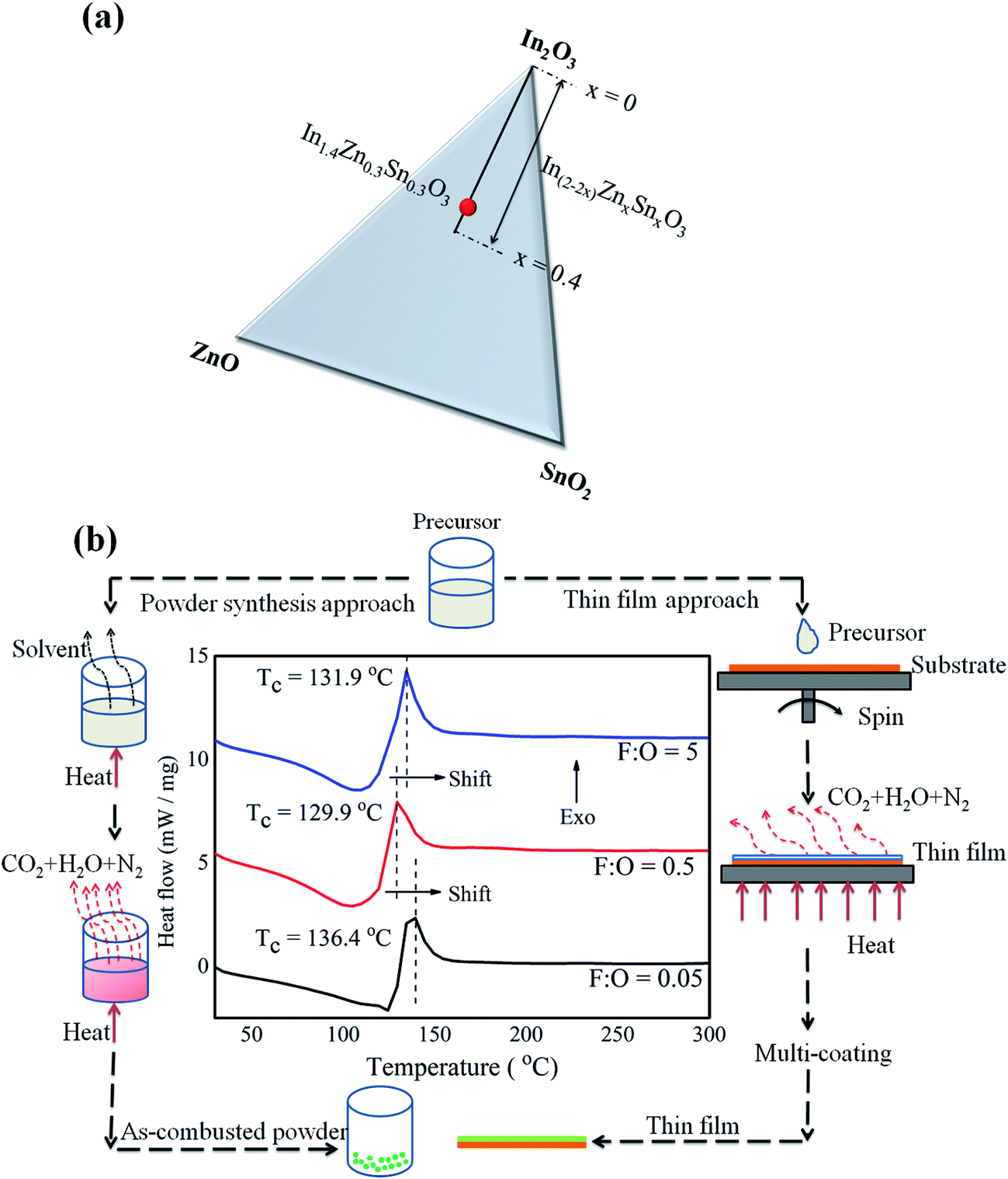 | ||
| Fig. 1 (a) Gibb's triangle of In2O3–ZnO–SnO2 ternary system showing stoichiometry of the present study. (b) Schematic of the processes employed and differential scanning calorimetric curves of precursors prepared with different F:O ratios. | ||
As-combusted powders were subjected to X-ray diffraction studies (Fig. 2a), just by looking at the pattern it is difficult to confirm whether the powder is amorphous or crystalline especially in case of F:O = 0.5 (Fig. 2a). In order to get a clear perspective; SAED patterns were recorded and found that fuel lean (Fig. 2b) and fuel rich (Fig. 2c) powders were crystalline in nature. But, in case of optimum redox mixture (Fig. 2d and e) the powder was mixture of amorphous and crystalline phases. The degree of crystallinity is less prominent in case of F:O = 0.5; thus no fringe pattern was observed (Fig. 2e). This may be due to amount of energy generated during combustion of precursors with balanced redox mixture. The heat energy may not be sufficient to make the powder complete crystalline; thus extra amount of energy needed for the complete crystallization. In addition, the colour of as-combusted powder in case of F:O = 5 is black; this may be due to retainment of unburnt excess carbon.
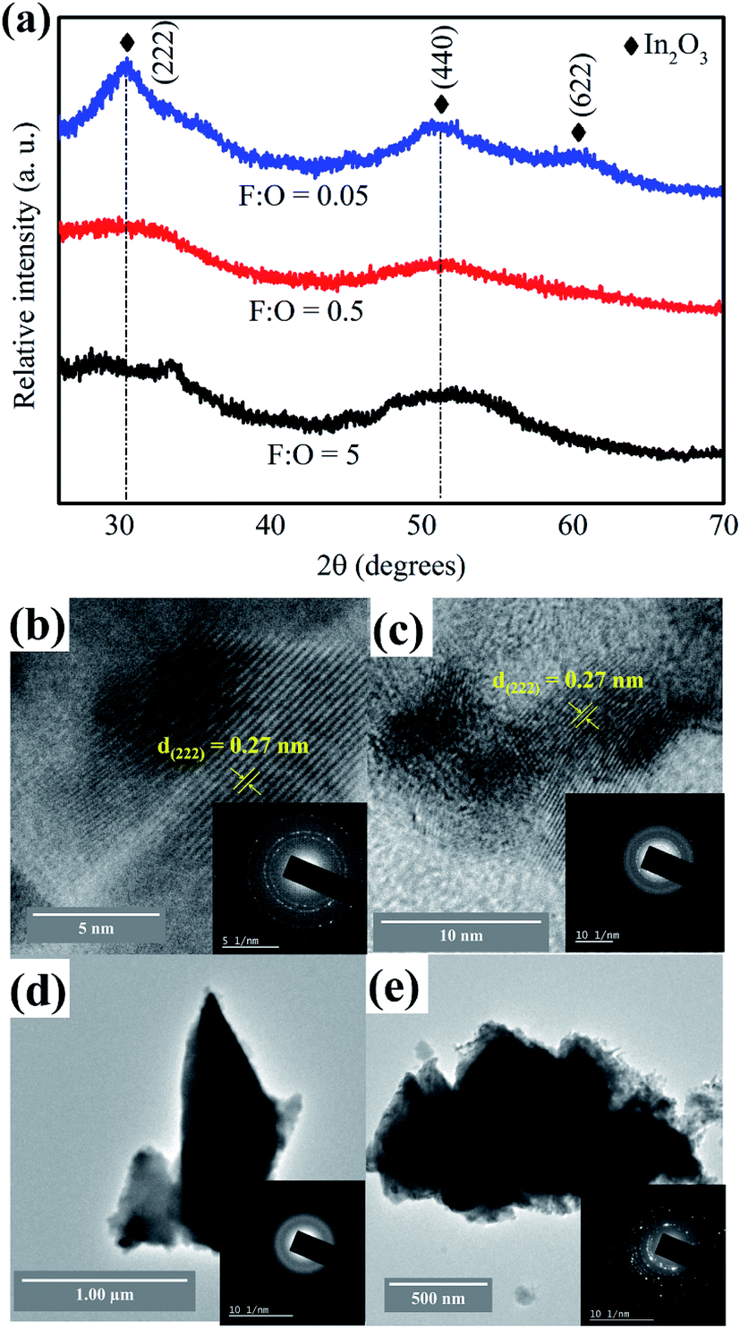 | ||
| Fig. 2 (a) XRD pattern of as-combusted powders with varying F:O ratios and TEM micrographs along with SAED patterns of powder with (b) F:O = 0.05; (c) F:O = 5; (d) and (e) F:O = 0.5. | ||
The as-combusted powders were further subjected to calcination for 2 h at 600 °C; and XRD pattern (Fig. 3a) of calcined powders show high degree of crystallinity with no secondary phases. The pattern perfectly matches with JCPDS: 00-006-0416 confirming the cubic bixbyite nature of the material. This implies, post doped structure retains original bixbyite of In2O3; which motivated us to develop unit cell of IZTO describing dopant positions using DFT (Fig. 3b).
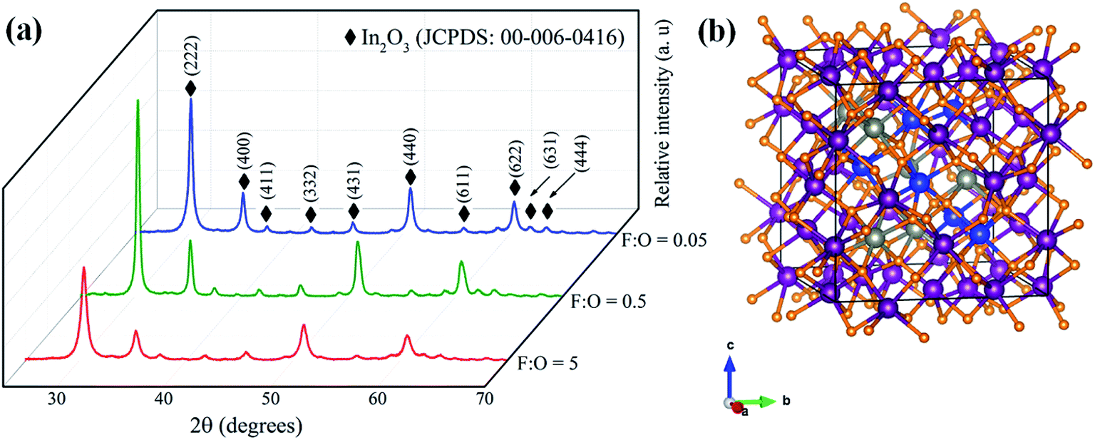 | ||
| Fig. 3 (a) XRD patterns of calcined IZTO powders with different F:O ratios. (b) Unit cell of IZTO with blue – tin, purple – indium, grey – zinc and orange – oxygen. | ||
Further, the precise lattice parameter of IZTO estimated using Nelson Riley function40 (for optimum F:O (= 0.5)) and compared with combustion derived In2O3 powder and found that there is slight increase (10.14 Å) in the value post doping compared to host In2O3 (10.11 Å), though the dopants Zn2+ (0.074 nm) and Sn4+ (0.069 nm) are of smaller size compared to In3+ (0.080 nm). The reported lattice parameter of IZTO is around 9.99 Å; which is much lower than the present value due to high temperature processing (1275 °C) with longer time (24 to 72 h).1 Whereas, in the present study calcination was carried out at 600 °C for 2 h; it might have resulted in the insufficient oxygen interstitials to balance repulsive forces originated from doping.10. (Details of calculation of lattice parameter using Nelson Riley function and combustion synthesis of In2O3 powder is addressed in ESI S2†).
The minimum combustion temperature and clean burning nature of precursor with optimum F:O (=0.5) grabbed our attention to fabricate thin film onto the glass substrate. All films annealed at different temperatures (200, 300 and 400 °C) were crystalline in nature (Fig. 4a) possessing bixbyite crystal structure but, when it is compared with low temperature combustion derived powder counterpart (Fig. 2a, XRD pattern of F:O = 0.5; as combusted powder) which is a mixture of both crystalline and amorphous phases. The decomposition of precursors and formation of doped oxides is different in case of thin films compared to bulk systems. In other words, combustion in a coated film has a different mechanism; because of large surface area of thin films.41 Thus it is important to study thin film materials as thin films rather than depending on their bulk counterparts.42 Although the combustion behavior on thin films is not clear,43 but the precursors having fuel-ligand (acetylacetone in this study) can yield crystalline thin films (Fig. 4a) at significantly low temperature (200 °C), which would have not been possible with conventional sol–gel precursors44 with large decomposition temperatures (>450 °C). Further, the film annealed at 200 °C shows considerable degree of transparency (83%) in the visible region (Fig. 4b) with an optical band gap of 4.2 eV (Fig. 4b; plot (eqn (3)))
| αhν = αo(hν − Eg)1/2, | (3) |
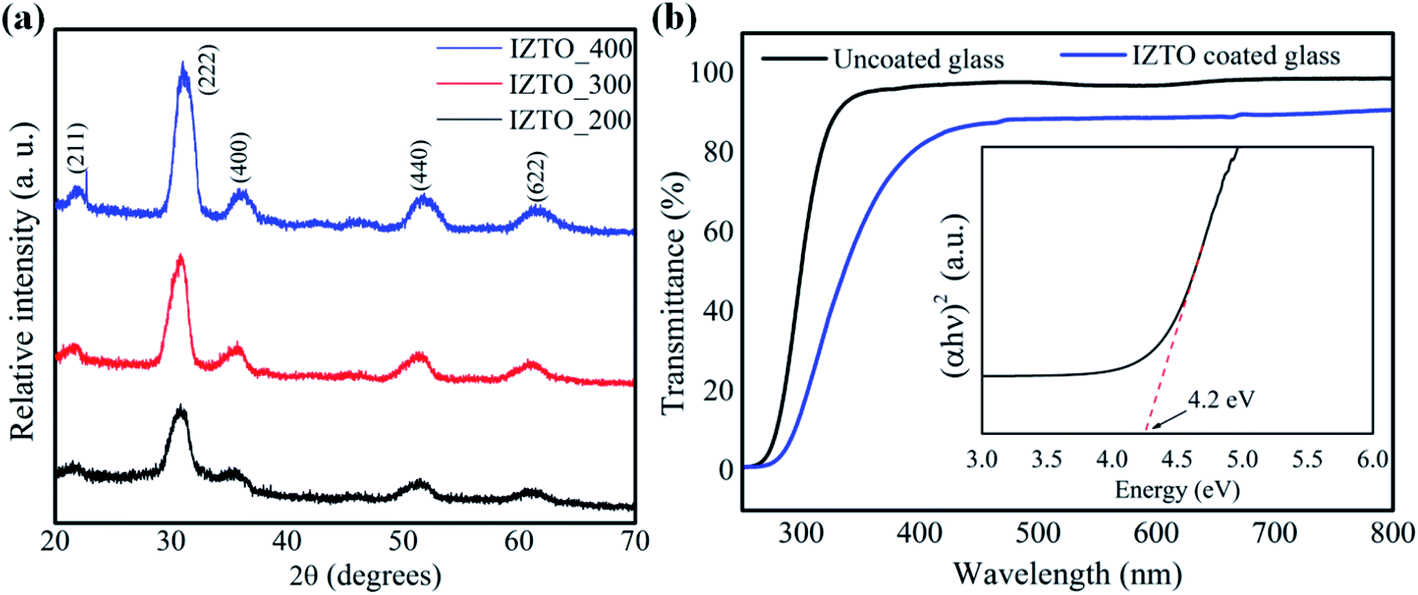 | ||
| Fig. 4 (a) GIAXRD plots of spin coated IZTO films annealed at different temperatures (b) UV-visible spectroscopic result of IZTO film (annealed at 200 °C) showing 83% transparency with optical and gap (inset). | ||
Further, in order to investigate the electronic properties of coated IZTO films; Hall effect measurements were carried out and found that the order of carrier concentration (N) was about 1019 cm−3 irrespective of annealing temperature (Fig. 5). It shows an increasing trend within the range of 3.7 × 10¹⁹ to 6.7 × 1019 cm−3; this clearly indicates the formation of vacancies contributing free charge carriers results in decrease in the resistivity (ρ) of the films (Fig. 5). The order of resistivity (10−2 Ω cm) especially at 200 °C is much lower than previously reported value for combustion derived ITO thin film;35 the improvement in the conductivity of the films is mainly guided by free charge carriers though there is small dip in the μH at 300 °C which doesn't have much effect on the overall resistivity of the IZTO at 300 °C.
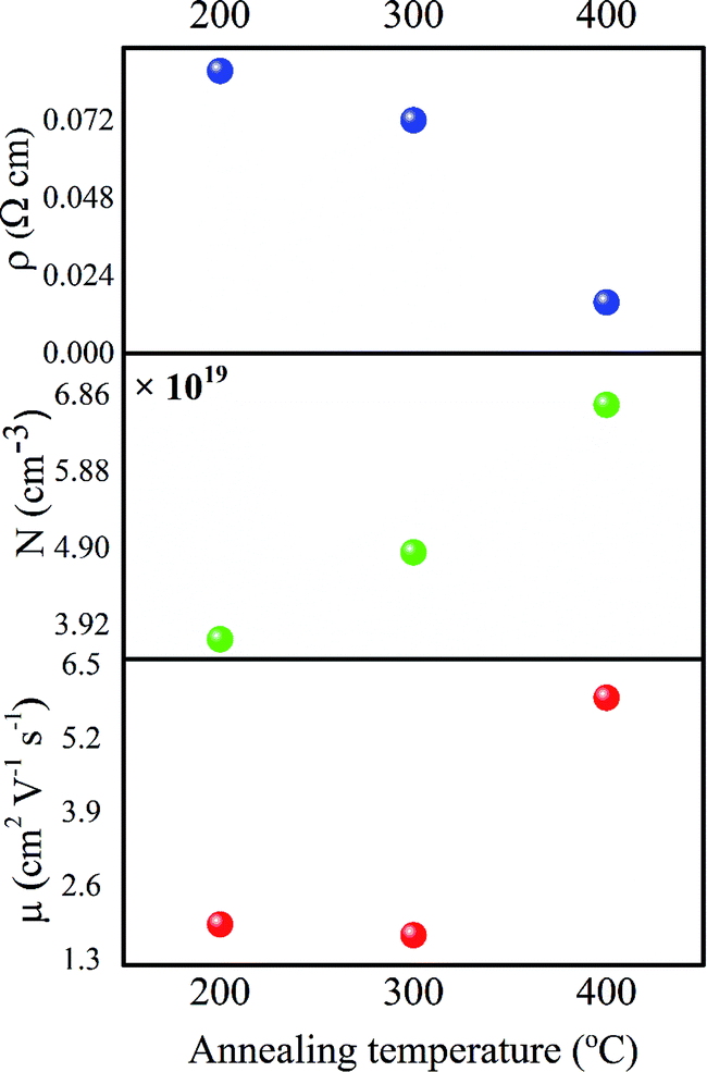 | ||
| Fig. 5 Hall effect measurements of IZTO thin films annealed at three different temperatures. | ||
In order to get more insight, X-ray photoelectron spectroscopic analysis of the films were carried out (Fig. 6). The full range scans (Fig. 6a) show indium, zinc, tin, oxygen and carbon signatures; source of trapped carbonaceous impurities might have come from unburnt carbon of the fuel, apart from the fact that the balanced redox mixture leaves no traces of unburnt hydrocarbon. One interesting thing about balanced reaction is that, it doesn't really takes care of secondary reactions such as decomposition of nitrates, hydrolysis etc. resulting in the continuous variation of F:O ratio45 as reaction progresses; consequence of which can be seen as the left out carbon trace resulting in scattering of the carriers; Fig. 6b shows exaggerated view of C 1s signature depicting fluctuations in the carbon impurity at 200 °C and 300 °C, but when annealed it at 400 °C is found that there is a drastic decrease in the intensity of the C 1s peak thereby reducing the scattering of the carriers. This can be clearly visualized from the μH results (Fig. 5), the slight decrease in the value from 200 to 300 °C (1.92 to 1.73 cm2 V−1 s−1) is due to fluctuations in the carbonaceous impurities, but when annealed at 400 °C the reduction of carbonaceous impurity (Fig. 6b) led to the sharp shoot-up in the μH from 1.73 to 5.92 cm2 V−1 s−1 (Fig. 5). Further, Fig. 6(c–e) shows deconvoluted O 1s peaks of films annealed at 200, 300 and 400 °C respectively; possessing principal signatures at 529 ± 0.5 eV corresponding M–O–M lattice,46 531.5 ± 0.5 eV depicting bulk and surface metal hydroxide species (M–OH),46 530 ± 0.5 eV corresponding O–adsorbates47 on the surface and additional signature (at 533.7 eV (ref. 48)) in the film annealed at 200 °C was observed (Fig. 6c). The Gaussian deconvoluted peaks give clear idea of precursor transformation into desired oxide.49 The ratio of intensities of these peaks (M–O–M/M–OH and M–O–M/O–adsorbates), as shown in the Fig. 6f, clearly convey the information that at low temperature the formation of M–O–M lattice is less pronounced compared to high temperature annealed films where there is a drastic increase of M–O–M/M–OH ratio from 200 °C to 400 °C can be supported by GIAXRD scans (Fig. 4a). It reflects the enhancement in the crystallinity with temperature, thus at high temperature the films are more of product oxides compared to films annealed at low temperature. The untransformed hydroxides are detrimental to the electrical performance of this film, that's the reason why the conductivity and the Hall mobility were considerably low at 200 °C, compared to high temperature annealed films. Formation lattice is the key for improved electrical performance of the film in terms of both mobility and generation of free carriers which contribute to electrical conductivity.
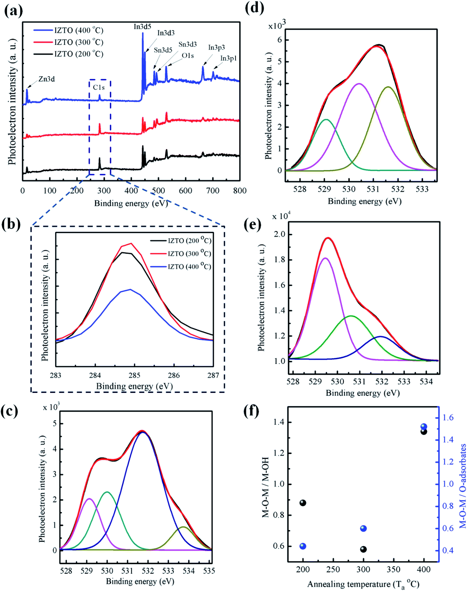 | ||
| Fig. 6 (a) XPS survey scan spectra obtained for IZTO films annealed at different temperatures (b) exaggerated view of C 1s signature. Deconvoluted O 1s peaks of IZTO annealed at (c) 200 °C (d) 300 °C and (e) 400 °C; (f) the intensity ratios of M–O–M/M–OH and M–O–M/O–adsorbates as a function of annealing temperature. | ||
The film annealed at 400 °C shows highest M–O–M/M–OH and M–O–M/M–OR ratios; which gives a clear evidence for the better quality of the film.
Also, the films annealed at different temperatures were smooth in nature with rms roughness below 2.42 nm (Fig. 7); at low temperature (200 °C) because of incomplete oxide formation led to slightly rough surfaces (Fig. 7) but with increase in the temperature the rms roughness shows smaller and values within the acceptable range (<1 nm).
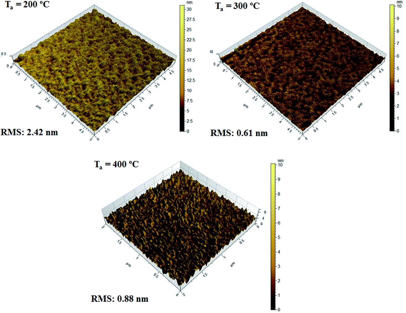 | ||
| Fig. 7 AFM results of IZTO films annealed at 200, 300 and 400 °C. | ||
As we have analyzed the quality and characteristics of films fabricated at low temperature; further we want to throw some light on the reason for the conducting nature of IZTO; Fig. 8 shows the electronic band structure of IZTO constructed using first principle DFT (refer Section 2.4) calculations which shows a direct band gap of 0.9 eV (Fig. 8). Calculated band gap is much smaller than the parent In2O3 band gap.50 This is mainly due to the impurity state from the doped atom present in the band gap energy region. Atom projected density of state of IZTO (ESI S3†) clearly shows the impurity trap states from doped Zn and Sn atom are present in the energy gap region, whereas the unfilled conduction states of In are 3.8 eV above the valence band maxima. Although optical band gap was found to be 4.2 eV (Fig. 4b), but electron could jump easily from the trap state to conduction band by overcoming a gap of 0.9 eV, is considered to be the main cause of conduction.
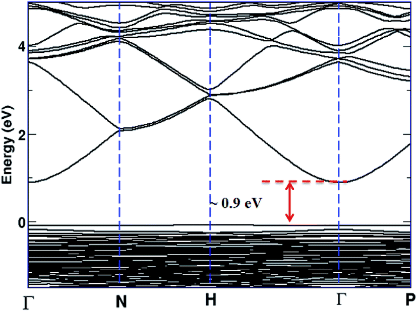 | ||
| Fig. 8 Electronic band structure of IZTO showing direct band gap of 0.9 eV. | ||
Further, the IZTO film on glass annealed at 400 °C is utilized for the fabrication of TFTs with following architecture glass/IZTO/PMMA/pentacene/Au, as shown in Fig. 9a. The capacitive response of PMMA dielectric as a function of frequency is illustrated in Fig. 9b. The output and transfer characteristics of TFT are as shown in the Fig. 9c and d. The electrical parameters such as μsat, Ion/Ioff ratio and VT were extracted from the transfer characteristics and determined to be 0.44 cm2 V−1 s−1 (from eqn (2)), 103 and −12.5 V, respectively. In addition, the hysteresis observed in both output and transfer characteristics was minimum (Fig. 9c and d). It shows the applicability of solution combustion derived IZTO to be used as a conducting film in an optoelectronic device.
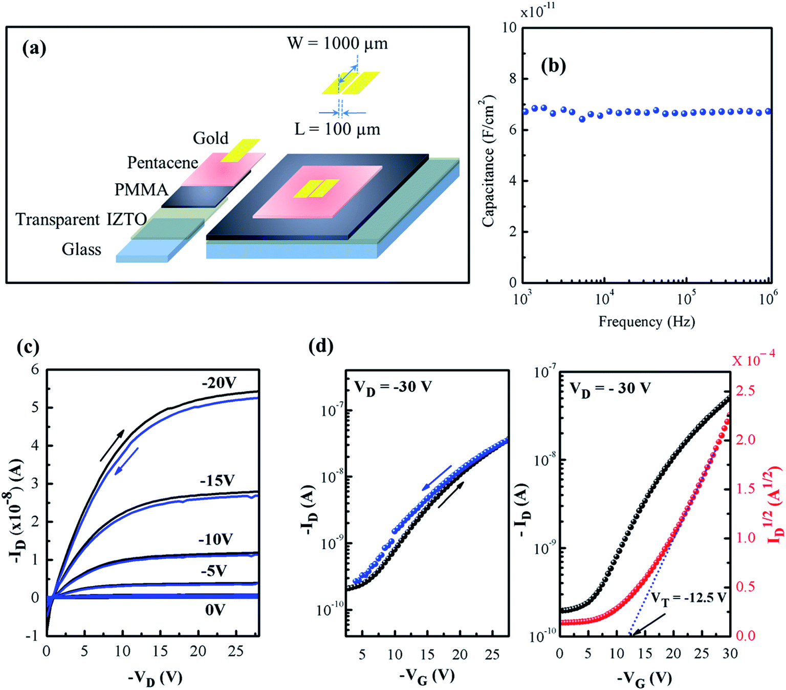 | ||
| Fig. 9 (a) Bottom gate top contact architecture, (b) capacitance vs. frequency of PMMA, (c and d) output and transfer (hysteresis) characteristics of TFT. | ||
Further, when it comes to highly transparent devices such as TFTs till date the most of the work was based on usage of metal contact electrodes which are opaque in nature and the body of the contact electrode pads are blind to the visible light there by decreases the overall transparency of the device. Recently, sol–gel derived cadmium oxide and aluminum doped cadmium oxide were inkjet printed51 using both 2-ME and aqueous based solutions and concluded that at low temperature 2-ME based solutions result in strong coffee ring deposits depicting high degree of edge deposits; but the present 2-ME based IZTO combustible precursor shows no such effect (Fig. 10a and b). It may be due to the presence of two different organic compounds (2-ME and acetylacetone-fuel) having different surface tension added with the pre-annealing temperature of 200 °C which helps in creating sufficient surface tension gradients there by supporting Marangoni inward flow suppressing edge deposit. Thus, it's possible to get dome (Fig. 10b) shaped printed feature in 2-ME based combustible precursor also. But, still more work has to be done in this area to establish strong base for 2-ME combustible precursor based printing; here in this contribution the possibility of anti-coffee ring deposit via 2-ME based system is demonstrated; which was recently proved best for aqueous sol–gel system.49 Moving on, the pre-annealed printed line feature was then subjected to high temperature of 400 °C and found that the conductivity shows a similar value as that of 400 °C annealed films via spin coating.
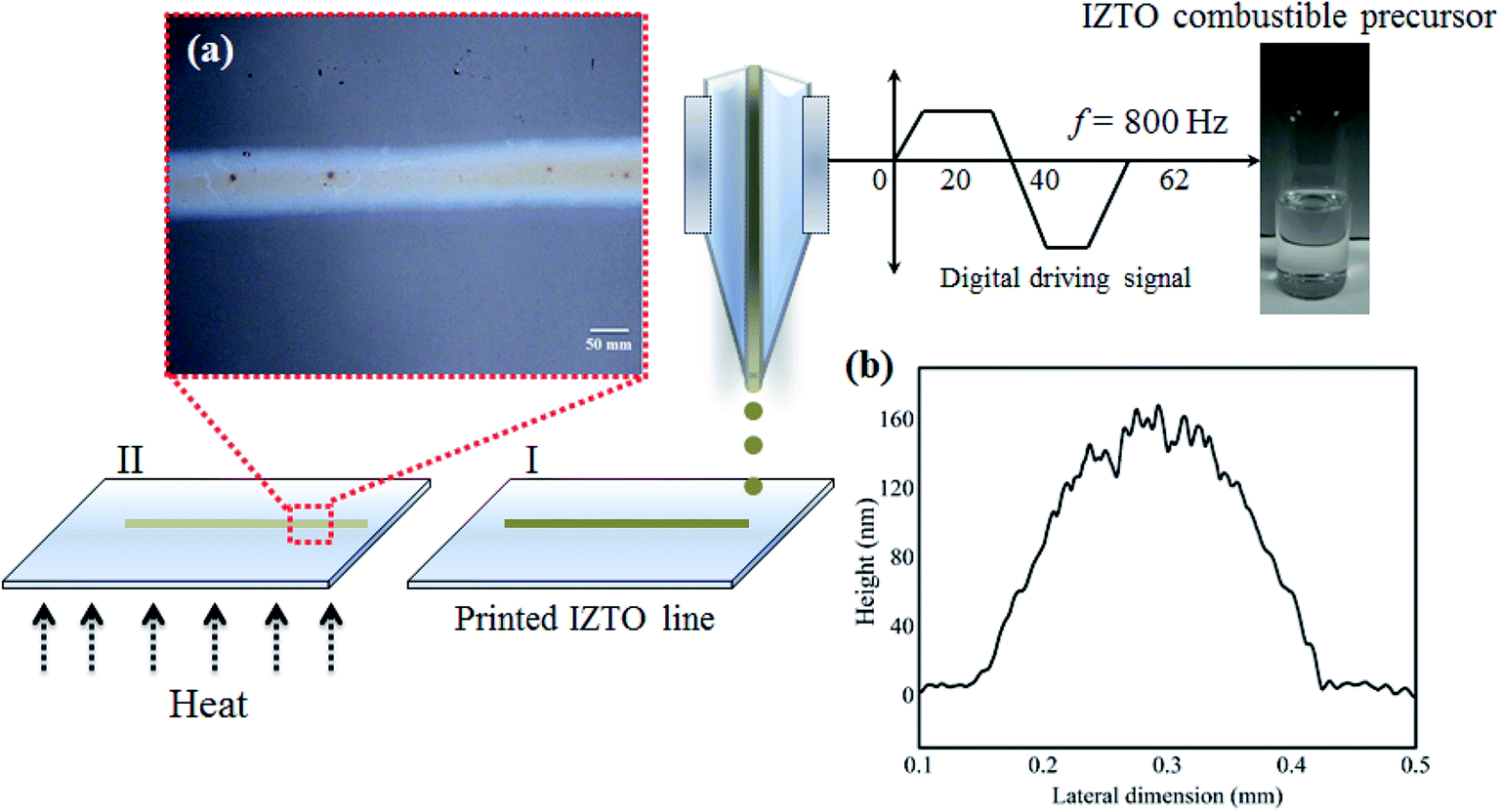 | ||
| Fig. 10 Printing of IZTO combustible precursor (a) printed IZTO line (b) line profile of printed line feature. | ||
4. Conclusions
A complex ternary conducting zinc tin co-doped indium oxide (IZTO – In1.4Sn0.3Zn0.3O3) is established in this study; solution combustion derived both bulk-powder and thin films were analyzed. In addition, initial trials of combustion reaction with varying F:O ratios depicted an optimum F:O derived from balanced redox mixture having minimal combustion temperature (∼130 °C) added with its clean burning behavior. Further, the film fabricated via same solution showed a decreasing trend in resistivity (of the order 10−2 Ω cm) with annealing temperature and highest μH of 5.92 cm2 V−1 s−1 at 400 °C with carrier concentration of 1019 cm−3 irrespective of annealing temperature. Also, the film (annealed at 200 °C) was transparent (83%) to the visible light; all IZTO films were smooth with rms values 2.42 nm, 0.61 nm and 0.8 nm at 200 °C, 300 °C and 400 °C respectively. The TFT fabricated using IZTO as one of its conducting component (gate electrode) with PMMA and pentacene as dielectric and active materials respectively has shown a μsat, Ion:Ioff and VT of 0.44 cm2 V−1 s−1, 103 and −12.5 V respectively with negligible hysteresis. Further, printability of combustion precursor was established and demonstrated the high quality of printed line feature with anti-coffee ring effect.
5. Author contribution
P. P., S. M., D. G. and Y. Y. N. designed experiments; K. T. developed both unit cell and band structure of IZTO; P. P. conducted experiments; S. G. and P. P. fabricated TFT and characterized; M. S. and P. P. optimized printing; B. G. and P. P. synthesized powders and analyzed. All authors read the manuscript and gave their valuable suggestions.Conflicts of interest
There are no conflicts to declare.Acknowledgements
This work is supported by Science and Engineering Research Board (SERB), Department of Science and Technology (DST) (ECR/2015/000339), DST – SB/S3/EECE/027/2013, DST – SB/FTP/PS-032/2014. We acknowledge, the Department of Metallurgical and Materials Engineering; NITK-Surathkal, and Department of Metallurgical Engineering and Materials Science (MEMS)-IIT Bombay, Centre for Excellence in Nanotechnology (CEN-IIT Bombay), IRCC, NCPRE – IIT Bombay; authors also extend regards to Amit Tewari (Research Scholar, IITB-Monash), PEEL-IITB.References
- S. P. Harvey, K. R. Poeppelmeier and T. O. Mason, J. Am. Ceram. Soc., 2008, 91, 3683–3689 CrossRef CAS.
- P. E. Burrows, G. L. Graff, M. E. Gross, P. M. Martin, M.-K. Shi, M. Hall, E. Mast, C. Bonham, W. Bennett and M. B. Sullivan, Displays, 2001, 22, 65–69 CrossRef CAS.
- G. Crawford, Flexible flat panel displays, John Wiley & Sons, 2005 Search PubMed.
- K. H. Choi, H. J. Nam, J. A. Jeong, S. W. Cho, H. K. Kim, J. W. Kang, D. G. Kim and W. J. Cho, Appl. Phys. Lett., 2008, 92, 223302 CrossRef.
- J. H. Bae, J. M. Moon, S. W. Jeong, J. J. Kim, J. W. Kang, D. G. Kim, J. K. Kim, J. W. Park and H. K. Kim, J. Electrochem. Soc., 2008, 155, J1–J6 CrossRef CAS.
- K. H. Lee, H. W. Choi, K. H. Kim and C. W. Bark, Mol. Cryst. Liq. Cryst., 2012, 567, 78–85 CrossRef CAS.
- W. S. Cheong, US Pat. 20130266724 A1, 2012.
- K. H. Choi, J. A. Jeong and H. K. Kim, Sol. Energy Mater. Sol. Cells, 2010, 94, 1822–1830 CrossRef CAS.
- J. H. Lee, H. S. Shin, S. I. Na and H. K. Kim, Sol. Energy Mater. Sol. Cells, 2013, 109, 192–198 CrossRef CAS.
- G. B. González, J. B. Cohen, J.-H. Hwang, T. O. Mason, J. P. Hodges and J. D. Jorgensen, J. Appl. Phys., 2001, 89, 2550–2555 CrossRef.
- Y. R. Denny, S. Seo, K. Lee, S. K. Oh, H. J. Kang, S. Heo, J. G. Chung, J. C. Lee and S. Tougaard, Mater. Res. Bull., 2015, 62, 222–231 CrossRef CAS.
- L. Raniero, I. Ferreira, A. Pimentel, A. Goncalves, P. Canhola, E. Fortunato and R. Martins, Thin Solid Films, 2006, 511, 295–298 CrossRef.
- C. Lee, R. Dwivedi, W. Lee, C. Hong, W. I. Lee and H. W. Kim, J. Mater. Sci.: Mater. Electron., 2008, 19, 981–985 CrossRef CAS.
- D. E. Proffit, T. Philippe, J. D. Emery, Q. Ma, B. D. Buchholz, P. W. Voorhees, M. J. Bedzyk, R. P. Chang and T. O. Mason, J. Electroceram., 2015, 34, 167–174 CrossRef CAS.
- H. C. Ma, M. Putri, J. H. Cheon, J. H. Kim and H. Y. Lee, J. Korean Phys. Soc., 2012, 61, 1994–1999 CrossRef CAS.
- A. Ambrosini, G. Palmer, A. Maignan, K. R. Poeppelmeier, M. Lane, P. Brazis, C. Kannewurf, T. Hogan and T. O. Mason, Chem. Mater., 2002, 14, 52–57 CrossRef CAS.
- M. G. Kim, H. S. Kim, Y. G. Ha, J. He, M. G. Kanatzidis, A. Facchetti and T. J. Marks, J. Am. Chem. Soc., 2010, 132, 10352–10364 CrossRef CAS PubMed.
- T. Minami, T. Kakumu, K. Shimokawa and S. Takata, Thin Solid Films, 1998, 317, 318–321 CrossRef CAS.
- Y. Shen, D. Jacobs, G. Malliaras, G. Koley, M. Spencer and A. Ioannidis, Adv. Mater., 2001, 13, 1234–1238 CrossRef CAS.
- A. Gurlo, Nanoscale, 2011, 3, 154–165 RSC.
- A. Gurlo, M. Ivanovskaya, N. Barsan and U. Weimar, Inorg. Chem. Commun., 2003, 6, 569–572 CrossRef CAS.
- A. Gurlo, D. Dzivenko, P. Kroll and R. Riedel, Phys. Status Solidi RRL, 2008, 2, 269–271 CrossRef CAS.
- H. Kim, C. Gilmore, A. Pique, J. Horwitz, H. Mattoussi, H. Murata, Z. Kafafi and D. Chrisey, J. Appl. Phys., 1999, 86, 6451–6461 CrossRef CAS.
- N. Bsiri, M. Zrir, A. Bardaoui and M. Bouaïcha, Ceram. Int., 2016, 42, 10599–10607 CrossRef CAS.
- S. Tabassum, E. Yamasue, H. Okumura and K. N. Ishihara, Appl. Surf. Sci., 2016, 377, 355–360 CrossRef CAS.
- Y. Choi, G. H. Kim, W. H. Jeong, H. J. Kim, B. D. Chin and J. W. Yu, Thin Solid Films, 2010, 518, 6249–6252 CrossRef CAS.
- C. Jin, I. K. You and H. K. Kim, Curr. Appl. Phys., 2013, 13, S177–S181 CrossRef.
- Y. Takahashi, S. Okada, R. B. H. Tahar, K. Nakano, T. Ban and Y. Ohya, J. Non-Cryst. Solids, 1997, 218, 129–134 CrossRef CAS.
- S. R. Ramanan, Thin Solid Films, 2001, 389, 207–212 CrossRef CAS.
- S. I. Na, B. K. Yu, S. S. Kim, D. Vak, T. S. Kim, J. S. Yeo and D. Y. Kim, Sol. Energy Mater. Sol. Cells, 2010, 94, 1333–1337 CrossRef CAS.
- H. C. Huang and T. E. Hsieh, Nanotechnology, 2010, 21, 295707 CrossRef PubMed.
- W. J. Park, H. S. Shin, B. Du Ahn, G. H. Kim, S. M. Lee, K. H. Kim and H. J. Kim, Appl. Phys. Lett., 2008, 93, 083508 CrossRef.
- Y. Y. Noh, X. Cheng, H. Sirringhaus, J. I. Sohn, M. E. Welland and D. J. Kang, Appl. Phys. Lett., 2007, 91, 043109 CrossRef.
- C. N. R. Rao, Chemical approaches to the synthesis of inorganic materials, John Wiley & Sons Inc, 1994 Search PubMed.
- M. G. Kim, M. G. Kanatzidis, A. Facchetti and T. J. Marks, Nat. Mater., 2011, 10, 382–388 CrossRef CAS PubMed.
- G. Kresse and J. Furthmüller, Comput. Mater. Sci., 1996, 6, 15–50 CrossRef CAS.
- G. Kresse and J. Furthmüller, Phys. Rev. B, 1996, 54, 11169 CrossRef CAS.
- P. E. Blöchl, Phys. Rev. B, 1994, 50, 17953 CrossRef.
- K. C. Patil, M. Hegde, T. Rattan and S. Aruna, Chemistry of nanocrystalline oxide materials – Combustion synthesis, properties and applications, World Scientific, New Jersey, 2008, ISBN 13 978-981-279-314-0 Search PubMed.
- C. Suryanarayana and M. G. Norton, X-ray diffraction: a practical approach, Springer Science & Business Media, 2013 Search PubMed.
- D. Sanchez-Rodriguez, J. Farjas, P. Roura, S. Ricart, N. Mestres, X. Obradors and T. Puig, J. Phys. Chem. C, 2013, 117, 20133–20138 CAS.
- S. R. Wood, K. N. Woods, P. N. Plassmeyer, D. A. Marsh, D. W. Johnson, C. J. Page, K. M. Jensen and D. C. Johnson, J. Am. Chem. Soc., 2017, 139, 5607–5613 CrossRef CAS PubMed.
- B. Wang, X. Yu, P. Guo, W. Huang, L. Zeng, N. Zhou, L. Chi, M. J. Bedzyk, R. P. Chang and T. J. Marks, Adv. Electron. Mater., 2016, 2, 1500427 CrossRef.
- Y. H. Kang, S. Jeong, J. M. Ko, J.-Y. Lee, Y. Choi, C. Lee and S. Y. Cho, J. Mater. Chem. C, 2014, 2, 4247–4256 RSC.
- R. Branquinho, D. Salgueiro, L. Santos, P. Barquinha, L. Pereira, R. Martins and E. Fortunato, ACS Appl. Mater. Interfaces, 2014, 6, 19592–19599 CAS.
- J. W. Hennek, J. Smith, A. Yan, M. G. Kim, W. Zhao, V. P. Dravid, A. Facchetti and T. J. Marks, J. Am. Chem. Soc., 2013, 135, 10729–10741 CrossRef CAS PubMed.
- H. Faber, Y. H. Lin, S. R. Thomas, K. Zhao, N. Pliatsikas, M. A. McLachlan, A. Amassian, P. A. Patsalas and T. D. Anthopoulos, ACS Appl. Mater. Interfaces, 2014, 7, 782–790 Search PubMed.
- S. Jeong, J. Y. Lee, S. S. Lee, Y. Choi and B. H. Ryu, J. Phys. Chem. C, 2011, 115, 11773–11780 CAS.
- M. Benwadih, R. Coppard, K. Bonrad, A. Klyszcz and D. Vuillaume, ACS Appl. Mater. Interfaces, 2016, 8, 34513–34519 CAS.
- F. Fuchs and F. Bechstedt, Phys. Rev. B, 2008, 77, 155107 CrossRef.
- W. J. Scheideler, R. Kumar, A. R. Zeumault and V. Subramanian, Adv. Funct. Mater., 2017, 27, 1606062 CrossRef.
Footnote |
| † Electronic supplementary information (ESI) available. See DOI: 10.1039/c7ra09189c |
| This journal is © The Royal Society of Chemistry 2017 |