
 Open Access Article
 This Open Access Article is licensed under a
 Creative Commons Attribution 3.0 Unported Licence
Flexible silver-mesh electrodes with moth-eye nanostructures for transmittance enhancement by double-sided roll-to-roll nanoimprint lithography
Peiyun Yi *a,
Chengpeng Zhanga,
Linfa Penga and
Xinmin Laiab
*a,
Chengpeng Zhanga,
Linfa Penga and
Xinmin Laiab
aState Key Laboratory of Mechanical System and Vibration, Shanghai Jiao Tong University, Shanghai 200240, P. R. China. E-mail: yipeiyun@sjtu.edu.cn
bShanghai Key Laboratory of Digital Manufacture for Thin-walled Structures, Shanghai Jiao Tong University, Shanghai 200240, P. R. China
First published on 17th October 2017
Abstract
Transparent conductive electrodes (TCEs) are an essential component in modern optoelectronic devices, such as touch panels, LCDs, OLEDs, and solar cells. Indium tin oxide (ITO), due to low sheet resistance and high transmittance, is still the dominant material for TCEs. However, its brittle nature and high cost hinder its future application in flexible devices, e.g., flexible displays, thin film solar cells, E-paper. Recently, patterned Ag-meshes have attracted wide attention from both academia and industry due to their excellent conductivity. Nevertheless, the transmittance is determined by gap area and restricts the further improvement of conductivity. This study proposes a novel approach to enhance the transmittance of Ag-mesh electrodes by moth-eye nanostructures which can be fabricated by double-sided roll-to-roll (R2R) nanoimprint lithography (NIL) simultaneously. Nickel mold and Anodic Aluminum Oxide (AAO) mold are developed for Ag-mesh girds and moth-eye nanostructures, respectively. A double-sided R2R NIL system is established and the novel Ag-mesh electrodes with moth-eye nanostructures have been fabricated. Sheet resistance, transmittance and flexibility performance have been evaluated systematically. An increase of 4.5% in transmittance has been achieved at a wavelength of 550 nm while remaining the sheet resistance at 22.8 ± 1.3 Ω sq−1. This research might provide a new approach for the large-scale and high through-output fabrication of high-transparency flexible Ag-mesh electrodes.
Introduction
Transparent conductive electrodes (TCEs) are an essential component in modern optoelectronic devices, such as touch panels, light-emitting diodes (LEDs) and solar cells, which require high optical transparency and high electrical conductivity, simultaneously.1–3 Indium tin oxide (ITO) has been studied for over fifty years and is widely used in industry due to its low sheet resistance and high transmittance.4,5 However, the brittle nature and high cost of the doping process pose potential challenges for future flexible device applications.6 Therefore, the development of alternative materials for future flexible device applications has caused the interests from both academia and industry. Different types of novel TCEs, including metal mesh, conductive nanowire, conductive polymers, carbon nanotubes, graphene, etc., have been reported successively.7–9 Among them, patterned silver (Ag)-mesh TCEs have exhibited high performance and show potential for commercialization in the near future.10,11To obtain the Ag-mesh TCEs, a large number of fabrication technologies have been proposed and developed in the past few years. Hu et al.12 reviewed various methods to fabricate the metal nanogrids for TCEs. Guo et al.13 pioneered nanoimprint lithography (NIL) for the fabrication of various metals and substrates and demonstrated excellent performance in the applications of solar cells and LEDs. Besides, they have developed large area continuous imprinting of nanogrids using their apparatus which was capable of roll-to-roll (R2R) printing on flexible web and roll-to-plate (R2P) printing on rigid substrates.14 Han et al.15 have fabricated the metallic networks TCEs based on the “cracked” gel film method. The fabrication process of metallic network TCEs mainly included four steps: synthesis and deposition of the TiO2 film (as a template film), self-cracking, metallic film deposition, and template film lift-off process. Besides, Kang et al.16 have adopted the capillary assembly of Ag nanoparticles along patterned nanogrid templates to fabricate the periodic Ag nanogrid electrodes. By using the high-aspect-ratio nanogrid template, the TCEs with high-aspect-ratio nanogratings can be obtained. Jin et al.17 adopted super-aligned carbon nanotubes as etching masks and fabricated large area nanoscale metal meshes. Since the metal meshes were fabricated as an integrated material, there was no junction resistance between the interconnected metal nanostructures, which markedly lowered their sheet resistance at high temperatures. Therefore, the metal meshes exhibited compatible performance in terms of optical transmittance and sheet resistance. Moreover, Huang et al.18 and Yao et al.19 have developed R2R apparatus for the high-throughput and high-accuracy fabrication of metal mesh electrodes. However, the advantage of patterned Ag-mesh results from the increased transparency relative to a continuous metal sheet since the area between grid lines is 100% transparent. The enhancement of transmittance comes at the price of an increase in sheet resistance which in turn depends on the width and spacing of mesh grids. Therefore, it is still a big challenge to improve the transmittance without increase of sheet resistance.
The moth-eye nanostructures are nipple arrays, typically of nano-scale height and diameter, which can reduce the reflectivity and increase the light transmission of the optoelectronic devices.20–22 More detailly, the moth-eye nanostructure arrays can make the refractive index (RI) of the surface layer vary gradually from air to substrate and therefore effectively suppresses the reflectance caused by the large refractive index discontinuity at the interface of two media. As a result, the moth-eye pattern has been applied in the solar cells successfully to enhance the light efficiency.23–27 Boden et al.23 have optimized the moth-eye pattern using rigorous coupled wave analysis and applied it in the silicon solar cells, including a laboratory cell (air–silicon interface) and an encapsulated cell (EVA–silicon interface). Han et al.25 fabricated a nanometer scale dot-pattern array by nano-imprint lithography process to reduce the reflection on the surface of GaInP/Ga(In)As/Ge solar cells. Rahman et al.28 have obtained highly regular surface nanotextures using the block copolymer self-assembly and plasma etching process. The size of fabricated nanotextures was in the range of 10–70 nm and could efficiently enhance the broadband antireflection in silicon solar cells. Zhou et al.27 reported an approach of optical manipulation of light by integrating a dual-side bio-inspired moth's eye nanostructure with broadband anti-reflective and quasi-omnidirectional properties. They observed that light out-coupling efficiency of OLEDs with stacked triple emission units was over 2 times of conventional one, resulting in drastic increase in external quantum efficiency and current efficiency. Murthy et al.29,30 investigated the fabrication and performance of broadband and omnidirectional antireflective polymer foils, in the visible spectrum (400–800 nm), which were fabricated by a high throughput roll-to-roll extrusion coating process. Although the moth-eye nanostructure array has been partially applied in the solar cells, its application in Ag-mesh TCEs for transmittance improvement has not been reported and the effects on Ag-mesh layer after the addition of the moth-eye nanostructure has not been investigated.
The Ag nanowire TCEs and Ag particle mesh TCEs are the most promising TCEs with potential for commercialization in the near future.31 The Ag particle mesh TCEs without moth-eye nanostructures that reported in our previous work show advantages in high-conductivity due to the direct metallic mesh patterning.32 However, the transparency of the thin-film was compromised due to the opacity of Ag-mesh. In order to develop a high-conductivity and high transparency TCEs thin-film, for the first time, the moth-eye pattern was introduced into the TCEs, which was based on the Ag nanowire and one-sided R2R NIL process.33 However, some disadvantage may exist in the Ag nanowire TCEs, such as poor binding force between the substrate and Ag nanowires. Therefore, the Ag particle mesh TCEs have been widely investigated, with Ag-mesh limited into the polymer structures. In this study, we report the development of Ag particle mesh TCEs with moth-eye nanostructures using the double-sided R2R NIL process. Through the double-sided R2R NIL process, the Ag-mesh structures and moth-eye nanostructures can be obtained simultaneously by one-step imprinting, which is very efficient. Firstly, nickel (Ni) mold and Anodic Aluminium Oxide (AAO) mold are developed for Ag-mesh girds and moth-eye nanostructures, respectively. A double-sided R2R NIL system is established and the novel Ag-mesh electrodes with moth-eye nanostructures have been fabricated. Sheet resistance, transmittance and flexibility performance have been evaluated systematically. This research aims to provide a new way for the transmittance improvement without increase of sheet resistance.
Experimental
Materials
Polyethylene terephthalate (PET) film, due to the characteristics of high transparency, good mechanical flexibility and low cost, has been selected as the substrate of flexible TCEs. The PET film with the thickness of 125 μm is produced by Jiangsu Kangde Xin Composite Material Co., Ltd. and the transmittance is 89% at the light wavelength of 550 nm. It should be pointed out that the film transmittance is not the highest one and might be improved with the decrease of film thickness. UV-curing resin LANG89A, provided by the same company, was a radical curing system resin and used for the fabrication of the polymer meshes and moth-eye nanostructures. The viscosity of UV resin is 322.3 cps. The Ag particle paste was purchased from NANO TOP Co., Ltd., which had an average particle diameter of 100 nm and 85% silver contents weight. The viscosity of Ag paste is 3500 cps which is much higher than UV resin.Mold fabrication
As shown in Fig. 1, the Ni mold for polymer meshes fabrication was obtained using the laser lithography technique and electroplating process.34 Briefly, in the laser lithography process, a layer of photoresist AZ4562 with the thickness of about 10 μm was spin coated on the glass substrate. After that, the photoresist layer was baked at the temperature of 95 °C for 25 min and then exposed in the Heidelberg DWL 66+ laser direct-writing system. The width and depth of narrow channels can be verified by adjusting the laser power and writing speed in laser scribing process. Finally, the master mold was transferred to Ni mold by electroplating process. In this study, the width and height of the gratings on the fabricated Ni mold were 7.3 ± 0.3 μm and 2.9 ± 0.1 μm, respectively.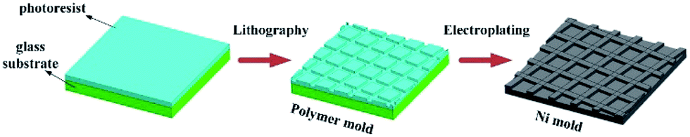 | ||
| Fig. 1 The schematic diagram for the fabrication process of mesh mold. | ||
The mold for moth-eye nanostructures fabrication was obtained by the AAO process, which was a cost-effective method for the nano-scale mold fabrication compared with the lithography-based method. And the nanopores with different diameters and depths can be obtained through the AAO process. The anodization process was carried out in 2 vol% phosphoric acid solution at 10 °C under the constant voltage of 120 V for 200 s each time with appropriate magnetic stirring. After anodization, the sample was dipped in 5 vol% phosphoric acid at 30 °C for 12.5 min to widen the holes. In this experiment, the AAO mold used for the fabrication of moth-eye nanostructures was about 90 nm in diameter, 100 nm in pitch, 180 nm in depth and 2 × 2 cm in area. Finally, the Ni mold for polymer meshes and AAO mold for moth-eye nanostructures was wrapped onto the forming roll in the R2R NIL system.
Fabrication of novel TCEs by R2R NIL process
A R2R UV-NIL system had been developed to fabricate micro/nano-scale structures continuously, which was suitable for both one-sided and double-sided imprinting, as described detailly in the previous literature.35 Two different kinds of flexible Ag-mesh TCEs were fabricated in this research to compare the difference in transmitting performance, the TCEs with and without moth-eye nanostructures. Fig. 2 showed the schematic diagram for fabrication of flexible Ag-mesh TCEs with and without moth-eye nanostructures. The flexible Ag-mesh TCEs without moth-eye nanostructures was accomplished by the one-sided R2R UV-NIL process and doctor blading of the Ag paste into the polymer meshes. The flexible Ag-mesh TCEs with moth-eye nanostructures was accomplished by a double-sided R2R UV-NIL process and doctor blading of the Ag paste into the polymer meshes. Both the two kinds of flexible Ag-mesh TCEs were produced by one-step imprinting, which was cost-effective and high-throughput. In this experiment, the imprinting process was carried out with feeding speed 0.5 m min−1, imprinting pressure 6 kg cm−2, tension force 12.5 kg and mold temperature 35 °C. The cured Ag meshes were eventually obtained after heated in an oven at the temperature of 135 °C for 30 minutes and then the Ag residual layer on the polymer surface was removed to improve the transparency of the electrodes by immersing the Ag meshes in nitric acid solutions (15 vol%) for 2 minutes.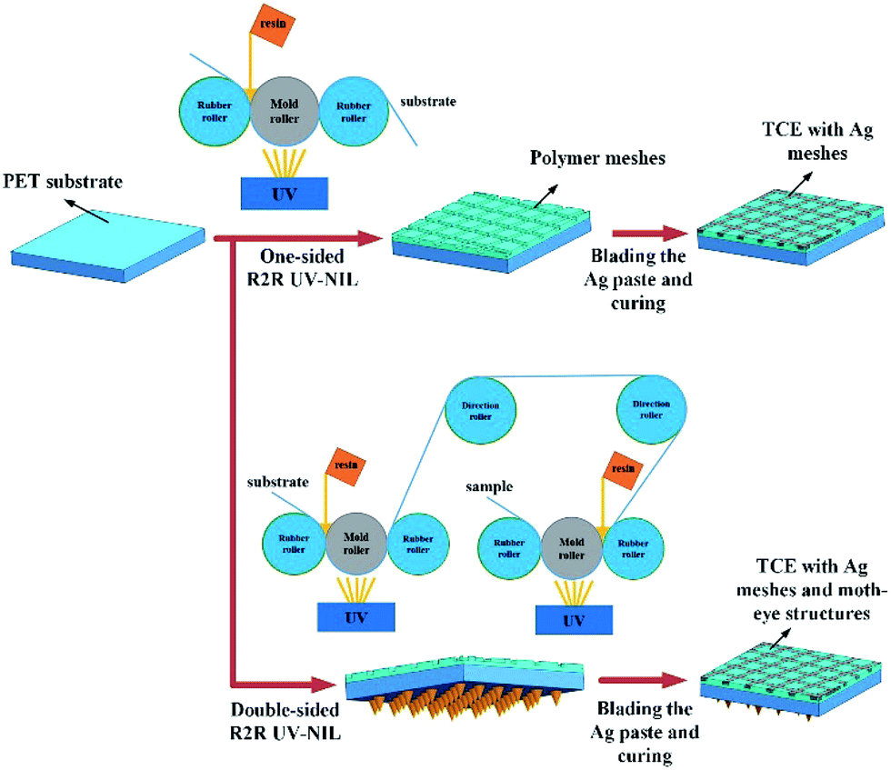 | ||
| Fig. 2 The schematic diagram for fabrication of flexible Ag-mesh TCEs with and without moth-eye nanostructures. | ||
Characterization
The polymer meshes were measured by a KEYENCE VK-X 200 laser confocal scanning microscopy. Atomic force microscope (AFM) images for the moth-eye nanostructures were obtained using a nanoscope scanning probe microscope (Dimension fast scan, Bruker, America) under ambient conditions. The scanning electron microscope (SEM) images for Ag-mesh TCEs were obtained using Zeiss Ultra Plus field emission scanning electron microscope with an electron energy of 5 kV. The sheet resistance were measured by using the four-probe technique with Loresta AX four point probe resistance meter MCP-T370. The transmittance spectra were recorded using a spectrophotometer (Shimadzu UV3600, Shimadzu, Japan) combined with an integrating sphere for the 400–800 nm wavelength range.Results and discussion
Structure and dimension
Fig. 3 presented the imprinting results of polymer meshes on the flexible PET substrate. As presented in Fig. 3(a) and (b), the polymer meshes showed excellent uniformity in the structures. The section analysis of the microscope images was used to measure the geometric parameters quantitatively and the width on the top surface was chosen as the width of the polymer meshes. The concave microchannels were 7.2 ± 0.3 μm in width and 2.8 ± 0.1 μm in depth, respectively, as shown in Fig. 3(c). The AFM images were used to analyse the moth-eye nanostructures, which could provide structural parameters of moth-eye nanostructures conveniently. Fig. 3(d) and (e) showed the 3-dimensional AFM images of the moth-eye nanostructures imprinted by the double-sided R2R UV-NIL process on the other side of the PET substrate. As shown in Fig. 3(e), the depth analysis of the AFM images was used for the height characterization of the moth-eye nanostructures and the maximum height values were chosen as the forming height of the moth-eye nanostructures. Herein, the diameter and height of the moth-eye nanostructures were 86.9 ± 2.3 nm and 165.2 ± 5.6 nm, respectively. Both for the polymer meshes and the moth-eye nanostructures, the values reported were averaged over different areas of the samples for at least five measurements.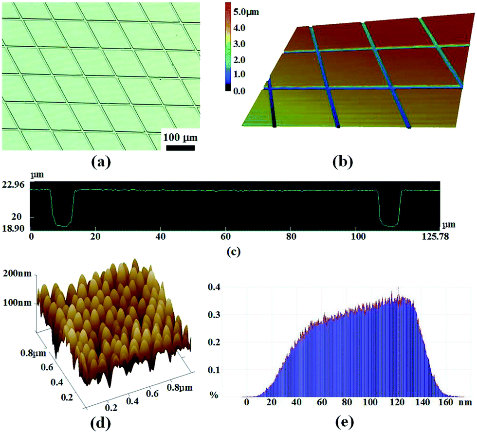 | ||
| Fig. 3 Measured results of polymer meshes and moth-eye nanostructures: (a) the 2-D image of polymer meshes, (b) the 3-D image of polymer meshes, (c) the section of polymer meshes, (d) the AFM image of moth-eye nanostructures, (e) the depth analysis of the AFM image. | ||
After the fabrication of polymer meshes and moth-eye nanostructures, the Ag particle paste was then coated on the concaves of polymer meshes to achieve conductive performance. In this experiment, a two-step doctor blading process was adopted to fully fill the polymer meshes with the Ag particle paste. After the first doctor blading, the Ag meshes was preheated in the oven at 135 °C for 3 min and then the second doctor blading followed. The cured Ag meshes was eventually obtained after heated in an oven at the temperature of 135 °C for 30 minutes. As shown in Fig. 4, the Ag particle paste was doctor bladed into the polymer meshes perfectly.
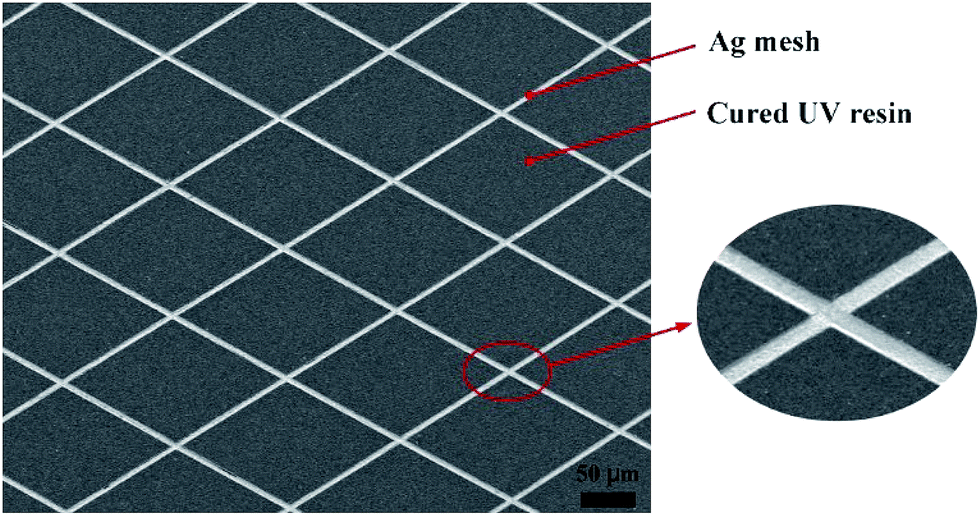 | ||
| Fig. 4 The SEM images of the Ag meshes fabricated by the R2R UV-NIL process. | ||
Sheet resistance
Basically, flexible TCES should have good conductivity to meet the requirements of low power density and rapid response time for optoelectronic applications. In this study, the average sheet resistance of the flexible Ag mesh TCEs was 22.6 ± 1.5 Ω sq−1, which was averaged over different areas of the samples for at least ten measurements. According to the public reports, the sheet resistance value can meet the requirements for the large-area displays.11,12 In conclusion, good electrical conductivity was accomplished for the flexible Ag-mesh TCEs in batch fabrication mode, which was obtained by the cost-effective and high-throughput R2R NIL process.Transmittance improvement
As one of the main performance criteria for the TCEs, high optical transmittance was also very critical.36 Fig. 5(a) compares the transmittance of the flexible Ag-mesh TCEs with and without moth-eye nanostructures, which is measured by the spectrophotometer at incident angles 8°. It is obvious that the transmittance has been increased after attaching moth-eye nanostructures. As the commonly used wavelength for visible light,37,38 the optical transmittance at wavelength of 550 nm was 81.4% and 85.9% for Ag-mesh TCEs without and with moth-eye nanostructures, respectively. An increase about 4.5% in transmittance was accomplished by attaching moth-eye nanostructures. Further, in order to investigate the omnidirectional performance of the moth-eye nanostructures, transmittance at different incident angles 0°, 10°, 30°, and 50° were measured by the variable angle spectroscopic ellipsometer (W-VASE with AutoRetarder™, America). As shown in Fig. 5(b), the transmittance at different incident angles 0°, 10°, 30°, and 50° show no obvious changes within the spectral ranges of 400–800 nm. Meanwhile, the average sheet resistance of flexible TCEs with moth-eye nanostructures was also measured, which was 22.8 ± 1.3 Ω sq−1, and nearly no changes were observed in the sheet resistance after the addition of moth-eye nanostructures. According to the experimental results, the addition of moth-eye nanostructures for Ag-mesh TCEs could significantly improve the transmittance performance while remaining the high electrical conductivity, which could provide a general strategy of preparing hetero-layers for the construction of high-performance electronic thin films for future flexible optoelectronics.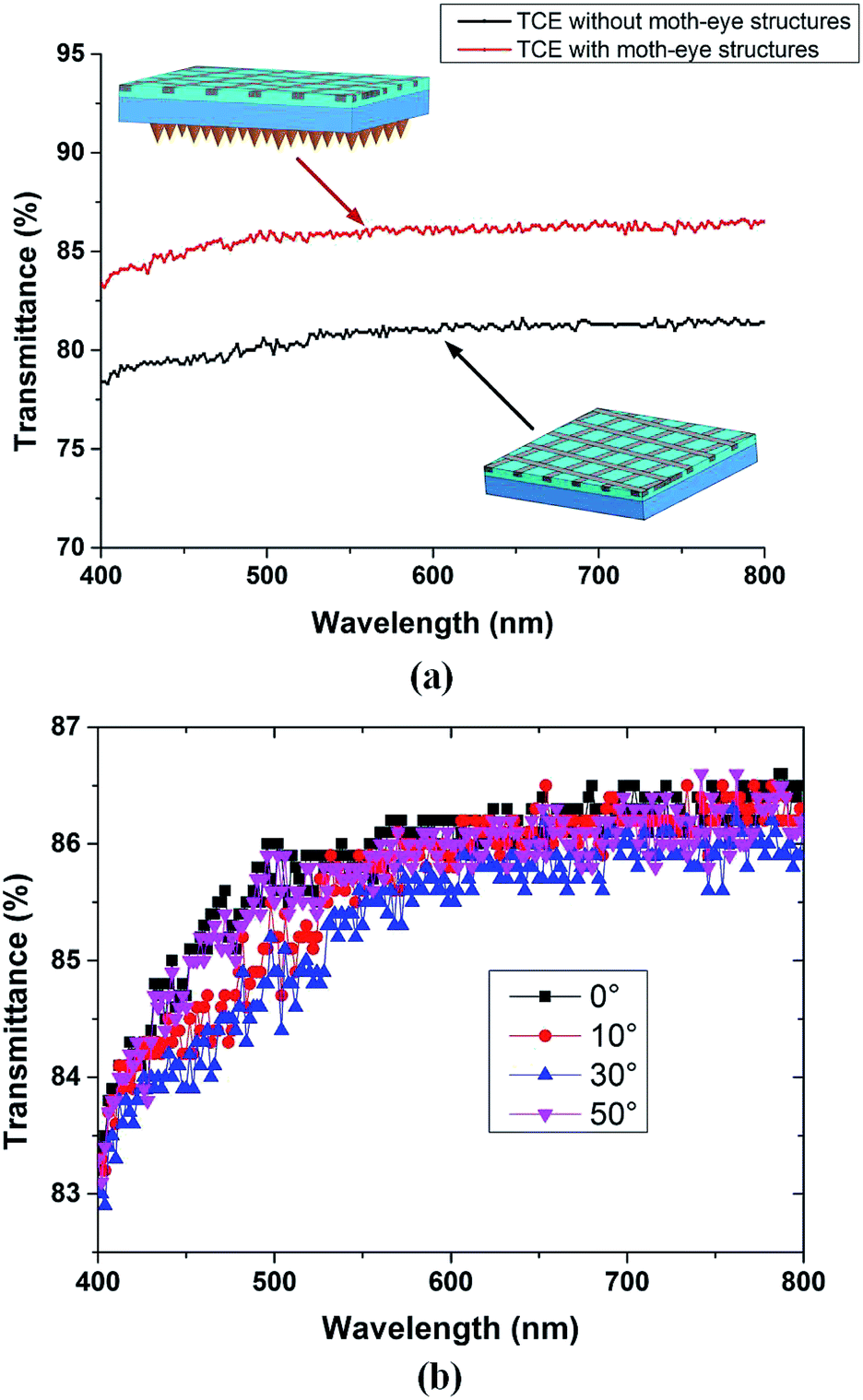 | ||
| Fig. 5 Optical performance: (a) transmittance of Ag-mesh TCEs with and without moth-eye nanostructures at incident angles 8°, (b) transmittance at different incident angles 0°, 10°, 30°, and 50°. | ||
Flexibility performance
To be used in the future flexible optoelectronic devices, the Ag-mesh TCEs should retain superior electrical conductivity and optical transmittance even after mechanical deformation. In this research, the sheet resistance and optical transmittance of the Ag-mesh TCEs with moth-eye nanostructures under different bending radii and different bending cycles were measured to evaluate the flexibility performance. Different bending cycles were accomplished through the screw system, stepping motor, and single-chip microcomputer control, which was presented in the previous literature.39 Moreover, both tensile test and compressive test were carried out in this study, as shown in Fig. 6(a) and (b). Fig. 6(c) showed the sheet resistance of Ag-mesh TCEs with moth-eye nanostructures under different bending radii and different bending cycles. It is obvious that, for the bending radius of 10 mm, the sheet resistance showed no obvious differences both in the tensile test and compressive test. Only a slight increase in the sheet resistance was observed after 1000 bending cycles and this indicated that the Ag-mesh TCEs with moth-eye nanostructures could retain superior electrical conductivity with larger bending radius, which was 10 mm in this experiment. The slight increase in sheet resistance might be attributed to the partial damage to the Ag meshes.17,40 Similarly, for the compressive bending radius of 3 mm, no noticeable change in sheet resistance was also observed after 1000 bending cycles. However, for the tensile bending radius of 3 mm, the noticeable change was observed, which might be attributed to the crack of Ag meshes after mechanical deformation.40–43 As shown in Fig. 6(d), the optical transmittance of the Ag-mesh TCEs with moth-eye nanostructures nearly remained unchanged under different bending radii and different bending cycles, indicating the moth-eye nanostructures were not damaged during the bending tests. Besides, a similar variation in the sheet resistance and optical transmittance of Ag-mesh TCEs without moth-eye nanostructures was also observed, which was not displayed in this research.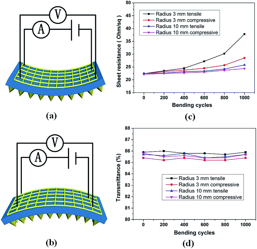 | ||
| Fig. 6 Flexibility performance of the Ag-mesh TCEs with moth-eye nanostructures: (a) schematic diagram of the compressive loading, (b) schematic diagram of the tensile loading, (c) the sheet resistance under different bending radii and different bending cycles, (d) the transmittance at the light wavelength of 550 nm under different bending radii and bending cycles. The values were all measured after the Ag-mesh TCEs were relaxed back to planar condition. | ||
Conclusions
Transparent conductive electrodes require high transmittance and low sheet resistance for large-scale optoelectronic devices. How to improve the transmittance without increase of sheet resistance is a big challenge for both academia and industry. This study proposed a novel approach to enhance the transmittance of Ag-mesh electrodes by integration of moth-eye nanostructures on the other side. The flexible Ag-mesh TCEs with moth-eye nanostructures were obtained by a one-step double-sided R2R UV-NIL process and scraping of the Ag paste into the polymer meshes. Sheet resistance, transmittance and flexibility performance have been evaluated systematically. The optical transmittance at wavelength of 550 nm was improved from 81.4% to 85.9% for Ag-mesh TCEs due to the effect of moth-eye nanostructures. The sheet resistance remained at 22.8 ± 1.3 Ω sq−1 and no obvious change has been observed due to the addition of moth-eye nanostructures. Besides, the bending tests indicated that the novel Ag-mesh TCEs with moth-eye nanostructures exhibited good flexibility performance. This research might provide a new approach for the large-scale and high through-output fabrication of high-transparency flexible Ag-mesh electrodes. It should be pointed out that the transmittance of Ag-mesh TCEs with moth-eye nanostructures might be improved further by optimizing the moth-eye nanostructures and adopting thinner substrate with higher transmittance in the future.Conflicts of interest
There are no conflicts to declare.Acknowledgements
This study was supported by the National Natural Science Foundation of China (51675334, 51235008).References
- D. S. Hecht, L. Hu and G. Irvin, Adv. Mater., 2011, 23, 1482–1513 CrossRef CAS PubMed.
- T. Sannicolo, M. Lagrange, A. Cabos, C. Celle, J.-P. Simonato and D. Bellet, Small, 2016, 12, 6052–6075 CrossRef CAS PubMed.
- L. Daniel, G. Gaël, M. Céline, C. Caroline, B. Daniel and S. Jean-Pierre, Nanotechnology, 2013, 24, 452001 CrossRef PubMed.
- R. Bel Hadj Tahar, T. Ban, Y. Ohya and Y. Takahashi, J. Appl. Phys., 1998, 83, 2631–2645 CrossRef CAS.
- C. G. Granqvist, Thin Solid Films, 2014, 564, 1–38 CrossRef CAS.
- A. Kumar and C. Zhou, ACS Nano, 2010, 4, 11–14 CrossRef CAS PubMed.
- S. Bae, H. Kim, Y. Lee, X. Xu, J.-S. Park, Y. Zheng, J. Balakrishnan, T. Lei, H. Ri Kim, Y. I. Song, Y.-J. Kim, K. S. Kim, B. Ozyilmaz, J.-H. Ahn, B. H. Hong and S. Iijima, Nat. Nanotechnol., 2010, 5, 574–578 CrossRef CAS PubMed.
- Z. Fan, X. Tao, X. Fan, X. Zhang and L. Dong, Carbon, 2015, 86, 280–287 CrossRef CAS.
- Z. Chai, J. Gu, J. Khan, Y. Yuan, L. Du, X. Yu, M. Wu and W. Mai, RSC Adv., 2015, 5, 88052–88058 RSC.
- J.-H. Min, S.-Y. Jang, K.-Y. Kim, S.-B. Choi, W.-S. Seong and D.-S. Lee, RSC Adv., 2015, 5, 75325–75332 RSC.
- K. Ellmer, Nat. Photonics, 2012, 6, 809–817 CrossRef CAS.
- L. Hu, H. Wu and Y. Cui, MRS Bull., 2011, 36, 760–765 CrossRef CAS.
- M.-G. Kang, H. J. Park, S. H. Ahn and L. J. Guo, Sol. Energy Mater. Sol. Cells, 2010, 94, 1179–1184 CrossRef CAS.
- S. H. Ahn and L. J. Guo, ACS Nano, 2009, 3, 2304–2310 CrossRef CAS PubMed.
- B. Han, K. Pei, Y. Huang, X. Zhang, Q. Rong, Q. Lin, Y. Guo, T. Sun, C. Guo, D. Carnahan, M. Giersig, Y. Wang, J. Gao, Z. Ren and K. Kempa, Adv. Mater., 2014, 26, 873–877 CrossRef CAS PubMed.
- J. Kang, C.-G. Park, S.-H. Lee, C. Cho, D.-G. Choi and J.-Y. Lee, Nanoscale, 2016, 8, 11217–11223 RSC.
- Y. Jin, Q. Li, M. Chen, G. Li, Y. Zhao, X. Xiao, J. Wang, K. Jiang and S. Fan, Nanoscale, 2015, 7, 16508–16515 RSC.
- Y. Huang, J. Chen, Z. Yin and Y. Xiong, IEEE Trans. Compon., Packag., Manuf. Technol., 2011, 1, 1368–1377 CrossRef CAS.
- O. Nezuka, D. Yao and B. H. Kim, Polym.-Plast. Technol. Eng., 2008, 47, 865–873 CrossRef CAS.
- Y. Li, J. Zhang and B. Yang, Nano Today, 2010, 5, 117–127 CrossRef.
- R. Brunner, O. Sandfuchs, C. Pacholski, C. Morhard and J. Spatz, Laser Photonics Rev., 2012, 6, 641–659 CrossRef.
- F. Buyukserin, M. Aryal, J. Gao and W. Hu, Small, 2009, 5, 1632–1636 CrossRef CAS PubMed.
- S. A. Boden and D. M. Bagnall, Prog. Photovoltaics, 2010, 18, 195–203 CAS.
- N. Yamada, O. N. Kim, T. Tokimitsu, Y. Nakai and H. Masuda, Prog. Photovoltaics, 2011, 19, 134–140 CAS.
- K.-S. Han, J.-H. Shin, W.-Y. Yoon and H. Lee, Sol. Energy Mater. Sol. Cells, 2011, 95, 288–291 CrossRef CAS.
- K.-S. Han, J.-H. Shin and H. Lee, Sol. Energy Mater. Sol. Cells, 2010, 94, 583–587 CrossRef CAS.
- L. Zhou, Q.-D. Ou, J.-D. Chen, S. Shen, J.-X. Tang, Y.-Q. Li and S.-T. Lee, Sci. Rep., 2014, 4, 4040 CrossRef PubMed.
- A. Rahman, A. Ashraf, H. Xin, X. Tong, P. Sutter, M. D. Eisaman and C. T. Black, Nat. Commun., 2015, 6, 5963 CrossRef CAS PubMed.
- S. Murthy, M. R. Lotz, N. Feidenhans'l, M. H. Madsen, H. C. Pedersen, H. Pranov and R. Taboryski, Macromol. Mater. Eng., 2017, 302, 1700027 CrossRef.
- S. Murthy, M. Matschuk, Q. Huang, N. K. Mandsberg, N. A. Feidenhans'l, P. Johansen, L. Christensen, H. Pranov, G. Kofod and H. C. Pedersen, Adv. Eng. Mater., 2016, 18, 484–489 CrossRef CAS.
- P. Gajendran, N. B. Devi and R. Devasenathipathy, Int. J. Electrochem. Sci., 2015, 10, 3301–3318 Search PubMed.
- Z. Wang, P. Yi, L. Peng, X. Lai and J. Ni, IEEE Trans. Nanotechnol., 2017, 16, 687–694 CrossRef.
- C. Zhang, Y. Zhu, P. Yi, L. Peng and X. Lai, J. Micromech. Microeng., 2017, 27, 075010 CrossRef.
- P. Linfa, Z. Chengpeng, W. Hao, Y. Peiyun, L. Xinmin and N. Jun, IEEE Trans. Nanotechnol., 2016, 15, 971–976 CrossRef.
- C. Zhang, P. Yi, L. Peng, X. Lai and J. Ni, IEEE Trans. Nanotechnol., 2015, 14, 1127–1137 CrossRef CAS.
- D. Langley, G. Giusti, C. Mayousse, C. Celle, D. Bellet and J.-P. Simonato, Nanotechnology, 2013, 24, 452001 CrossRef PubMed.
- W.-K. Kim, S. Lee, D. Hee Lee, I. Hee Park, J. Seong Bae, T. Woo Lee, J.-Y. Kim, J. Hun Park, Y. Chan Cho, C. Ryong Cho and S.-Y. Jeong, Sci. Rep., 2015, 5, 10715 CrossRef CAS PubMed.
- B. Deng, P.-C. Hsu, G. Chen, B. N. Chandrashekar, L. Liao, Z. Ayitimuda, J. Wu, Y. Guo, L. Lin, Y. Zhou, M. Aisijiang, Q. Xie, Y. Cui, Z. Liu and H. Peng, Nano Lett., 2015, 15, 4206–4213 CrossRef CAS PubMed.
- C. Zhang, P. Yi, L. Peng, X. Lai, J. Chen, M. Huang and J. Ni, Sci. Rep., 2017, 7, 39814 CrossRef CAS PubMed.
- Y. Jiang, J. Xi, Z. Wu, H. Dong, Z. Zhao, B. Jiao and X. Hou, Langmuir, 2015, 31, 4950–4957 CrossRef CAS PubMed.
- K. D. Harris, A. L. Elias and H. J. Chung, J. Mater. Sci., 2016, 51, 2771–2805 CrossRef CAS.
- M.-S. Lee, J. Kim, J. Park and J.-U. Park, Nanoscale Res. Lett., 2015, 10, 27 CrossRef PubMed.
- A. Vazinishayan, S. Yang, A. Duongthipthewa and Y. Wang, AIP Adv., 2016, 6, 025006 CrossRef.
| This journal is © The Royal Society of Chemistry 2017 |