
 Open Access Article
 This Open Access Article is licensed under a
 Creative Commons Attribution 3.0 Unported Licence
A high performance supercapacitor based on decoration of MoS2/reduced graphene oxide with NiO nanoparticles
F. Ghasemia,
M. Jalalia,
A. Abdollahiab,
S. Mohammadic,
Z. Sanaeeb and
Sh. Mohajerzadeh *a
*a
aNanoelectronic Lab, School of Electrical and Computer Engineering, University of Tehran, Tehran, 14399-56191, Iran. E-mail: mohajer@ut.ac.ir
bNanofabricated Energy Devices Lab, School of Electrical and Computer Engineering, University of Tehran, Tehran, 14399-56191, Iran
cFaculty of Engineering Science, College of Engineering, University of Tehran, Tehran, 11155-4563 Iran
First published on 15th November 2017
Abstract
In this report, the capacitive performance of molybdenum disulfide (MoS2) and reduced graphene oxide (rGO) supercapacitors and the effect of NiO nanoparticle incorporation is investigated. A comparison between rGO, MoS2, and MoS2/rGO sheets revealed that the MoS2/rGO composite exhibited higher capacitance owing to better charge transfer in comparison to its individual counterparts. The incorporation of NiO nanoparticles was feasible through sputter deposition of 10 nm NiO film, which upon thermal annealing converted into nanostructures with an average grain size of 35 nm. The NiO-decorated MoS2/rGO electrode showed superior capacitance performance compared to non-decorated samples. The thermal treatment of NiO film was performed at 350 °C in the presence of argon gas for 30 min. The final capacitance of the a:NiO/rGO and a:NiO/MoS2/rGO electrodes was significantly enhanced to 4.8 and 7.38 mF cm−2, respectively, compared with individual rGO (2.31 mF cm−2) or MoS2 (1.01 mF cm−2) electrodes at the same scan rate of 25 mV s−1. Moreover, the a:NiO/MoS2/rGO electrode exhibited a long discharging time of 34.5 s with promising cycle stability (about 90%) over 1000 cycles.
1. Introduction
The search for clean and renewable energy is regarded as a major challenge for researchers and related communities.1 Consequently, materials and devices for energy storage and conversion have received significant attention since renewable energy sources are in high demand.2,3 To date, various types of energy generating and storage devices such as solar cells,4 fuel cells,5 batteries6 and supercapacitors7 have been introduced. Among these, supercapacitors have been considered as important devices because of their high power density, fast charge–discharge ability and long cycling life-time.8 Numerous materials have been investigated to be utilized in supercapacitor electrodes, including carbon based structures,9 conducting polymers,10 transition metal oxides11 and metal hydroxides.12The excellent physical properties of graphene (as a carbon based material) as well as good energy transport and storage potential make it a promising candidate for supercapacitor applications.13 However, low volumetric capacitance and low gravimetric energy density are the main drawbacks of graphene based energy devices.14 In order to overcome this issue, hybrid based graphene materials such as conductive polymers, metal oxide nanoparticles, and transition metal dichalcogenide (TMDs: MoS2, WS2, WSe2) nanosheets have been employed to refine the capacitance capability.15,16 Conducting polymers, however, suffer from poor cycling stability, inactive electrochemical surface area and unwanted swelling/shrinking deformation during the charge–discharge process, which results in reduced performance.17 On the contrary, TMDs possess unique physical and electrochemical properties suitable for charge storage and practical capacitors.18 The hexagonal layered structure of TMD crystals is composed of metal atoms (Mo, W, and Ti) sandwiched between two chalcogen atoms (S, Se) held together via van der Waals (vdW) interaction.19 As the most promising TMD structure, molybdenum disulfide (MoS2) demonstrates novel semiconductor properties with great prospect for futuristic energy applications.20 The high amount of intrinsic fast ionic conductivity and oxidation states in layered MoS2 structures propound them as desired candidates for charge storage devices.21
To date, different approaches have been introduced to prepare few-layered MoS2 structures such as mechanical exfoliation,22 solvent based exfoliation23 and chemical vapour deposition24 (CVD) growth. Solvent based sonication-assisted exfoliation is considered as a superior technique to provide few-layered MoS2 structures in NMP, DMF and other solvents owing to its simplicity, reliability, and low cost of production.25 Our recently reported solvent exchanged sonication technique provided a high yield production of large lateral size MoS2 few layers.26 Although the low conductivity of pure MoS2 limits its capacitance performance, its hybrid structure with rGO possesses higher capability for charge storage.27
Moreover, a variety of metal oxide structures such as RuO2, IrO2, and NiO have been presented as pseudocapacitor electrodes with outstanding electrochemical potentials.28,29 The high chemical stability, low production cost, environment-friendly nature, and availability of NiO structures open up an unprecedented opportunity for NiO material to serve as an energy storage device.30 Despite all these benefits, the high intrinsic electrical resistance of NiO material limits its individual usage for electrochemical utilizations, which requires its combination with other electrically conductive materials.31
In this paper, the as-fabricated MoS2 dispersion was drop-casted on reduced graphene oxide nanosheets (MoS2/rGO) and subsequently decorated with 10 nm annealed sputtered NiO film (a:NiO). GO sheets were prepared using modified Hummer's method, followed by thermal reduction treatment at 850 °C under 90 mTorr pressure of H2 gas.32 MoS2 nanosheets were also produced with the aid of solvent sonication of bulk material based on our introduced solvent exchange method.26 Moreover, NiO thin film with 10 nm thickness was deposited on both rGO and MoS2/rGO electrodes and annealed at 350 °C for 30 min under a flow of argon gas. The thermal energy imparted during annealing converts the NiO thin film into NiO nanoparticles on the electrode surfaces. Incorporation of NiO nanoparticles into the given electrodes leads to remarkable enhancement of capacitance electrodes. For instance, at the scan rate of 25 mV s−1, capacitance values of 1.01, 2.31, 3.74, 4.8, and 7.38 mF cm−2 were achieved for MoS2, rGO, MoS2/rGO, a:NiO/rGO, and a:NiO/MoS2/rGO electrodes, respectively. These results are comparable or superior to other reported capacitance values for rGO hybrid supercapacitors (Table 1). In addition, the a:NiO/MoS2/rGO electrode demonstrated a high discharging time of 34.5 s (compared with other electrodes) with an excellent life cycle over a 1000-cycle test.
| Electrode | Electrolyte | Area capacitance | Reference |
|---|---|---|---|
| a:NiO/MoS2/rGO | 1 M KCl | 7.38 mF cm−2 (at 25 mV s−1) | This study |
| rGO–GO–rGO | 0.1 M NaClO4 | 2 mF cm−2 | 43 |
| Light scribed GO | PVA–H2SO4 | 2.9 mF cm−2 (at 50 mV s−1) | 61 |
| rGO–CNT | 3 M KCl | 6.1 mF cm−2 (at 10 mV s−1) | 58 |
| CNT/MoO3 | 1 M HCl | 4.86 mF cm−2 (at 10 mV s−1) | 56 |
| Graphite oxide | 1 M Na2SO4 | 0.51 mF cm−2 (at 20 mV s−1) | 57 |
| MoS2 nanoparticles | 0.5 M H2SO4 | 29 μF cm−2 (at 0.5 mV s−1) | 59 |
| Graphene/CNT | 1 M Na2SO4 | 2.16 mF cm−2 (at 100 mA cm−2) | 64 |
| Exfoliated MoS2 | 6 M KOH | 2 mF cm−2 (at 10 mV s−1) | 60 |
2. Experimental
2.1. Materials
Graphite powder was supplied by Fluka (99.9% purity). MoS2 powder (lateral size of ∼50 μm, 99% purity), IPA solvent, sodium nitride (NaNO3), sulfuric acid (H2SO4), potassium permanganate (KMnO4), and hydrogen chloride (HCl) were acquired from Sigma Aldrich. NMP and DMF solvents were purchased from Merck Company. All materials were used with no special purification.2.2. Preparation of graphene oxide sheets
Two grams of graphite powder and one gram of NaNO3 were mixed into a flask in an ice-water bath containing 46 mL H2SO4 and the temperature was maintained below 20 °C. Then, 6 g potassium permanganate (KMnO4) was gradually added to the flask and the mixture was continuously stirred for 30 min at a constant temperature of 35 °C. The obtained suspension was diluted with 92 mL de-ionized water, followed by the addition of 340 mL H2O2. The pale brown colour of the aqueous solution referred to the successfully oxidized graphite flakes. In order to remove the residual metal ions and acids in the solution, the dispersion was diluted with HCl (10%) and centrifuged at 3000 rpm for 60 min. The resulting sediments were re-dispersed in distilled water and centrifuged again. Finally, the residual sediments were dispersed in de-ionized water and sonicated for 2 h in an ultrasonic bath (at 100 W) to exfoliate graphite oxide into GO nanosheets. After sonication, the dispersion was centrifuged at 3000 rpm for 30 min to eliminate unexfoliated flakes, and subsequently the top supernatant was collected, containing mostly few layered GO nanosheets.2.3. Preparation of MoS2 nanosheets
MoS2 nanosheets were prepared by two-step sonication in DMF and NMP solvents based on our previous report. In this method, 0.5 g bulk MoS2 powder was mixed with 10 mL NMP in an ice-bath and sonicated for 15 min at 400 W. After centrifugation (60 min, 4000 rpm), the top supernatant was collected and diluted with IPA, accompanied with 30 min centrifugation at 1000 rpm. Next, the prepared solution was placed in a vacuum oven for 24 h at 70 °C in order to evaporate the solvent. Finally, 10 mL DMF was added to the remaining dried MoS2 flakes and sonicated for further 15 min at a power of 400 W.2.4. Preparation of MoS2/rGO electrode
After placing rGO layers on a Si substrate, 20 μL of acquired MoS2 dispersion was drop-casted on the rGO electrodes and dried at room temperature.2.5. Characterization
Field emission scanning electron microscopy imaging was performed using Hitachi, S-4160 FESEM (20 kV). Transmission electron microscopy (Philips CM 300 operated at 150 kV) was employed to analyse the size and crystallinity of layers. Atomic force microscopy (AFM) images were obtained using the NT-MDT system with the NSG30 resonant tip. UV-Visible and Raman spectra analyses were carried out utilizing UV/Vis PG Instrument Ltd and Senterra instrument (532 nm laser excitation). Moreover, X-Ray Diffraction (XRD) measurement was performed using the X'Pert PRO MPD system (X-ray source: Al Kα, 1.5406 Å, pressure > 10−7 Pa). A current–voltage parameter analyser (Keithly K361, USA) was used to measure the I–V characteristics of GO and rGO layers. Cyclic Voltammetry (CV) measurements were conducted using a three-electrode system (counter: a platinum rod electrode; reference: a standard Ag/AgCl electrode; working: rGO, MoS2, MoS2/rGO, a:NiO/rGO, and a:NiO/MoS2/rGO as-prepared electrodes) in 1 M KCl aqueous solution. To investigate the supercapacitance of the as-fabricated electrodes, CV measurements were carried out in a potential window between −0.6 V and 0.6 V at various scan rates of 25, 50, 100, and 200 mV s−1. Furthermore, a current density of 0.2 mA cm−2 was set for galvanostatic charging/discharging test of the as-prepared electrodes.3. Results and discussion
3.1. GO, rGO, and MoS2 characterizations
GO nanosheets were prepared by modified Hummer's method through oxidizing natural graphite powder via strong oxidizing agents (H2O2, H2SO4, KMnO4).32 By introducing hydroxyl and epoxy groups into graphite layers, van der Waals interaction was considerably decreased, leading to an easy exfoliation of stacked layers in ultrasonic processes.33 Fig. 1a shows an optical image of the resulting GO solution in di-ionized water containing few-layered sheets. MoS2 nanosheets were also achieved using the two-step exfoliation method presented by our group in the previous report.26 In this technique, the bulk MoS2 powder was exfoliated in NMP solvent at 400 W power sonication (7 s “on” and 3 s “off”) for 15 min and then centrifuged. In order to remove the unexfoliated flakes, the dispersion was diluted with a poor solvent (IPA) and subsequently subjected to low speed centrifugation.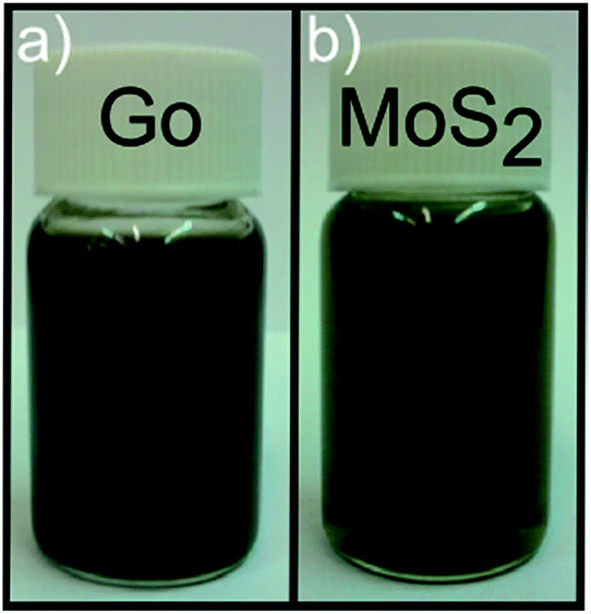 | ||
| Fig. 1 Optical images of the (a) prepared GO solution in di-ionized water. (b) MoS2 dispersion in DMF solvent. | ||
Then, the NMP/IPA mixture was evaporated in a vacuum oven and the resultant MoS2 flakes were collected. At the final step, DMF solvent was added to the dried flakes, followed by further 15 min-sonication at 400 W power, leading to the final optimal dispersion of few-layered MoS2 sheets. An optical image of the prepared MoS2 suspension in DMF solvent is demonstrated in Fig. 1b with a final concentration of 12 mL mg−1 as reported in our previous study.26
The morphology of GO and exfoliated MoS2 sheets, using SEM, TEM, and AFM analyses, is demonstrated in Fig. 2. As shown in the TEM images, the GO sheets are wrinkled, suggesting efficient exfoliation of bulk graphite (Fig. 2a). Correspondingly, selected area electron diffraction (SAED) reveals the good crystallinity of the layered GO.34 Fig. 2b presents the TEM image of a transparent MoS2 nanosheet, possessing high degree of crystallinity with a hexagonal six-fold symmetry (inset of Fig. 2b). To investigate the morphology of the GO layers, the obtained aqueous solution was drop-casted on a silicon substrate followed by drying at 80 °C. The SEM image of GO sheets shows curled configuration of layers distributed over the Si substrate (Fig. 2c) and the cross-sectional image also presents a layer by layer structure of the stacked GO sheets implying a good amount of expansion of bulk graphite into exfoliated layers (Fig. 2d). Moreover, based on the AFM analysis, the thickness of one few layered GO sheet is measured to be ∼3 nm, corresponding to 4 or 5 layers of GO as its monolayer has ∼0.7–0.8 nm thickness35 (Fig. 2e). The SEM image of the exfoliated MoS2 nanosheets is shown in Fig. 2f, demonstrating successful exfoliation of the bulk powder. In order to record a SEM image of MoS2 flakes, 20 μL droplets of the as-fabricated MoS2 suspension were deposited on a Si substrate and dried at 70 °C in a vacuum oven to completely remove its residual solvent.
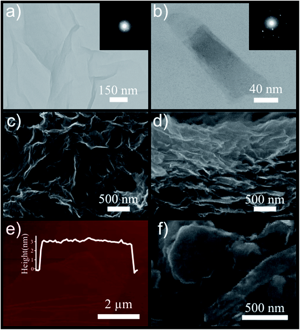 | ||
| Fig. 2 GO, rGO, and MoS2 characterizations: (a) Transmission Electron Microscopy (TEM) image of graphene oxide. Inset shows the diffraction pattern of layer. (b) TEM image of MoS2 nanosheets with the corresponding diffraction pattern (inset). (c) Scanning electron microscopy (SEM) image of GO sheets on Si substrate. (d) Cross-sectional SEM image of stacked GO sheets on Si substrate. (e) Atomic force microscopy (AFM) image of one few layered GO sheet with height profile of ∼3 nm. (f) SEM image of exfoliated MoS2 nanosheets. | ||
As reported in the literature, GO sheets possess low electrical conductivity (known as insulator) due to the presence of oxygen-functionalized compounds such as hydroxyl, carboxyl, and epoxy groups in their basal structures.36 Removing these functional groups would lead to reduced graphene oxide with unbonded conjugated electrons and considerably higher electrical conductivity.36 For this reason, a variety of reduction techniques have been suggested, such as thermal,36 chemical,37 UV assisted38 and electrochemical39 reduction methods. In detail, chemical reduction strategies take advantage of some strong reducing agents (hydrazine, lithium aluminium hydride, sodium borohydride, etc.) in order to reduce the GO sheets.37 Due to their poisoning hazards and re-agglomeration tendency, these conventional reductants introduce unwanted nitrogen bonds into the surface of the obtained rGO, which considerably affects the final electrical property of layers.40 Moreover, the UV assisted reduction method has been considered as an easy and green method;38 however prolonged UV exposure with low degree of reduction is the main drawback of this technique.40 The electrochemical reducing approach is also considered as an energy-consuming and high cost method.40 In contrast, the thermal reduction technique has a superior potential to reduce GO sheets by means of annealing (100–1100 °C) in H2, Ar, N2 or even vacuum media.36,40 In this study, GO sheets are reduced to rGO using 60 min thermal treatment at 850 °C in the presence of hydrogen gas. For this purpose, the as-fabricated GO dispersion was drop-casted on bare silicon substrates and dried at 80 °C for 24 h. Then, the samples were placed in a vacuum quartz furnace and heated up to 850 °C with a ramp rate of 10 °C min−1 under 15 sccm hydrogen flow under 90 mTorr chamber pressure. The samples were maintained at this state for 60 min and then cooled down to room temperature under almost identical conditions (110 mTorr pressure, 20 sccm hydrogen flow, 15 °C min−1). To characterize the reduction of GO sheets, electrical conductivity, Raman Spectroscopy, and X-ray diffraction (XRD) measurements were performed for both GO and rGO samples. GO sheets possess a high resistance of 10 MΩ (inset shows higher applied biasing voltages), which drops to 1 kΩ for rGO sheets owing to the elimination of oxygen-containing functional groups36 (Fig. 3a). Moreover, the Raman spectra of the samples show two characteristic peaks at 1340 cm−1 and 1580 cm−1, referring to the D and G peaks, respectively36 (Fig. 3b). As reported in the literature, G mode is assigned to the E2g phonon oscillation, while the D peak contributes to the sp2 breathing mode of carbon atoms.41 The ratio of D band intensity to G band intensity is a good parameter in assessing the reduction of GO sheets.42 According to the spectra, the ID/IG ratio decreases from 0.962 for GO to 0.950 for rGO, correspondingly. Decrease in intensity ratio is due to the reduction of surface-functionalized groups in the basal honeycomb structure of rGO in comparison to GO sheets.42 The XRD patterns of GO and rGO sheets are illustrated in Fig. 3c. The XRD pattern of GO sheets possesses a (002) peak centred at ∼10.8° corresponding to the interlayer spacing of 8.185 Å whereas that of rGO sheets have this peak located at 24.6°, attributed to the inter-planar distance of 3.615 Å.36 Indeed, the elimination of surface functional groups in thermal treated GO sheets is responsible for decrease in the inter-layer spacing value of rGO compared to GO sheets. The UV-Visible and Raman spectra of few-layered MoS2 are displayed in Fig. 3d. Two characteristic absorption peaks at 608 and 668 nm originate from direct band transition at K-point of the MoS2 Brillouin zone.26 Furthermore, the Raman spectrum of few-layered MoS2 reveals two in-plane and out-of-plane phonon scattering peaks (E12g, A1g) located at ∼386 and ∼404 cm−1, confirming effective exfoliation of the bulk material26 (inset of Fig. 3d).
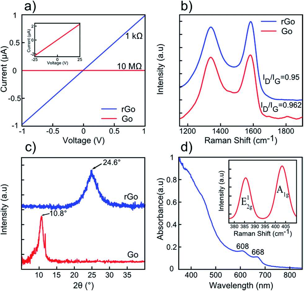 | ||
| Fig. 3 GO, rGO, MoS2 characterizations: (a) I–V characteristic of GO vs. rGO sheets. (b) Raman spectra of GO and rGO with their corresponded ID/IG ratios. (c) XRD patterns of GO and rGO sheets. (d) UV-Visible absorption spectrum of MoS2 few layers in DMF suspension prepared by a three-step technique with two direct transitions around 608 and 688 nm. Inset shows the corresponding Raman spectra of few layered sheets. | ||
In addition to rGO and MoS2, a 20 μL MoS2 dispersion was drop casted on the rGO/Si sample and characterized by SEM, current–voltage characterization, XRD, and Raman spectroscopy. Fig. 4a shows the SEM image of the MoS2/rGO sample, in which it could be observed that MoS2 nanosheets are well distributed over rGO sheets. The electrical conductivity of the MoS2/rGO/300 nm SiO2/Si sample is presented in Fig. 4b with approximately similar resistance as compared to the rGO sample. Moreover, the XRD pattern exhibits both diffraction peaks of MoS2 and rGO (∼24°), while Raman spectroscopy shows five peaks corresponding to MoS2 (∼386, 404 cm−1), Si (∼520 cm−1), and rGO (∼1340 and 1580 cm−1) oscillation modes.
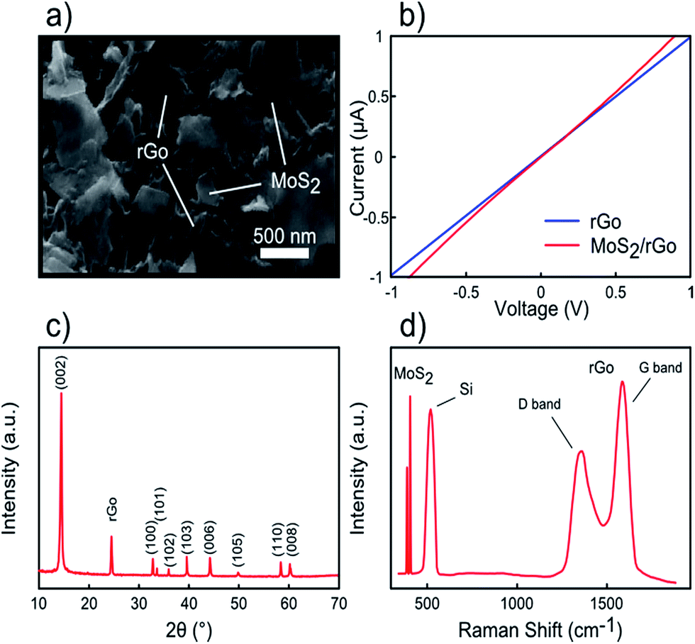 | ||
| Fig. 4 MoS2/rGO characterizations. (a) FESEM image of MoS2/rGO layers. (b) I–V curve of MoS2/rGO sheets. (c) XRD pattern of MoS2/rGO. (d) Raman spectrum of MoS2/rGO layers on a Si substrate. | ||
Fig. 5 displays the conventional cyclic voltammetry (CV analysis) curves of the rGO, MoS2, and MoS2/rGO (drop-casted MoS2 on rGO) electrodes at room temperature over different scan rates of 25, 50, 100, and 200 mV s−1 within a potential window between −0.6 V and +0.6 V in 1 M KCl electrolyte. All the CV curves have quasi-rectangular shapes, showing good capacitor behaviour without any redox peaks even at high scan rates.43 It is worth noticing that the lack of redox peaks indicates the contribution of electric double-layer capacitance (EDLC) behaviour, which in turn leads to reversible and considerably fast charge–discharge performances of electrodes.43 It is observed that higher area is obtained by increasing the scan rates, however, lower values for capacitance are obtained due to ineffective interaction between the electrolyte ions and the electrode.44 For the MoS2 electrode (Fig. 5b), the CV curves are nearly elliptical in shape (instead of quasi-rectangular), which can be assigned to weak redox reactions originating from variation of Mo oxidation states during the cyclic voltammetry process.45 At the same scan rate (100 mV s−1), it is observed that the MoS2/rGO electrode reveals better capacitance performance compared to either individual electrodes (Fig. 5d). The capacitance values as function of scan rate are derived for all three different electrodes by integrating the resultant CV curves (Fig. 5e). As shown in Fig. 5e, the increase in scan rate results in decrease in capacitance because of ion transport limitation near the electrodes.44 As observed, the rGO–MoS2 sample demonstrates the highest capacitance capability of 3.74 mF cm−2 (at a scan rate of 25 mV s−1), whereas rGO and MoS2 display lower values of 2.31 and 1.01 mF cm−2, respectively. The galvanostatic charge/discharge (GCD) curves of rGO, MoS2, and MoS2/rGO samples at a similar current density of 0.2 mA cm−2 are displayed in Fig. 5f. All samples show triangular and symmetric charging/discharging curves without considerable internal resistance, which is consistent with the expected double layer behaviour of electrodes.45 Among these samples, the MoS2/rGO electrode possesses the longest discharging time (17.83 s), corroborating the results of CV measurements.
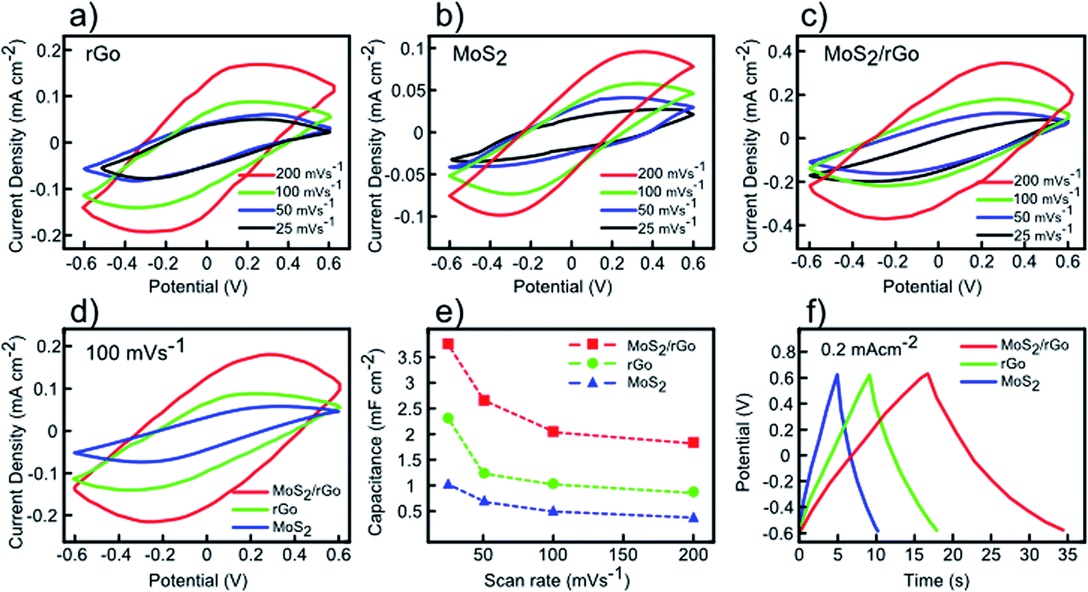 | ||
| Fig. 5 CV and GCD characterizations of the rGO, MoS2, and MoS2/rGO electrodes. (a) CV curve of rGO electrode at different scan rates (b) CV curves of MoS2 electrode at different scan rates (c) CV curves of MoS2/rGO electrode at different scan rates. (d) Comparison of rGO, MoS2, and MoS2/rGO CV curves at same scan rate of 100 mV s−1. (e) Area capacitance of rGO, MoS2, and MoS2/rGO electrodes as a function of scan rate. (f) GCD curves of rGO, MoS2, and MoS2/rGO electrodes at current density of 0.2 mA cm−2. | ||
3.2. rGO–NiO supercapacitor performance
In the previous section, rGO-based supercapacitor was investigated along with that based on MoS2 layers. The results showed that drop-casting a 20 μL MoS2 solution on the rGO electrode yielded high capacitance performance (MoS2/rGO) compared to other individual electrodes. In this section, we discuss the fabrication and electrochemical performance of a supercapacitor based on the few-layered rGO decorated with NiO nanoparticles. A schematic of the preparation process of rGO-decorated NiO nanoparticles is depicted in Scheme 1. NiO nanoparticles were acquired with the aid of thermal annealing of sputtered NiO thin film in argon ambient. For this purpose, a few droplets of the as-fabricated GO suspension were drop-casted on a Si substrate followed by drying the sample in an oven at 80 °C. Then, similar to the previous section, GO sheets were reduced to rGO layers through thermal treatment at 850 °C in H2 ambient (Scheme 1a). In the next step, 10 nm NiO film was deposited on the rGO sheets using the RF sputtering system (13.56 MHz frequency, 10−6 Torr pressure, 99.9% purity NiO target) as shown in Scheme 1b. The thickness of sputtered NiO film was measured using LSE-WS stokes WAFERSKAN Ellipsometer system. In order to convert the thin film NiO (tf:NiO) into nanoparticles, the prepared rGO–NiO thin film was placed in a vacuum quartz furnace and heated up to 350 °C under 15 sccm flow of argon gas, maintained for 30 min at this temperature and then cooled down to room temperature under the same conditions. Thermal annealing resulted in the conversion of tf:NiO to annealed-NiO (a:NiO) configuration without any changes in the phase-structure of rGO and NiO (Scheme 1c).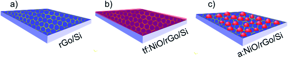 | ||
| Scheme 1 Schematic of (a) rGO sheets on a Si substrate. (b) Sputtered NiO film on the prepared rGO electrode. (c) Decoration of rGO layers with NiO nanoparticles after annealing at 350 °C for 30 min under 15 sccm argon flow. | ||
Fig. 6a presents the SEM image of the as-prepared a:NiO/rGO sample by 30 min-thermal annealing at 350 °C in the presence of argon gas. The as-obtained NiO nanoparticles are well-distributed over rGO sheets owing to the uniform deposition of the NiO film and optimal thermal annealing of the sputtered film. The size distribution of the NiO nanoparticles is measured to be around 10–100 nm with an average of 35 nm (inset of Fig. 6a). An AFM image of the a:NiO/rGO electrode is shown in Fig. 6b with the corresponding height profile of the NiO nanoparticles on the rGO layer. Moreover, Raman spectroscopy was carried out to investigate the evolution of two characteristic peaks of GO sheets (ID/IG ratio) during thermal annealing at 850 °C, deposition of NiO film, and thermal annealing of the sputtered film at 350 °C (Fig. 6c). According to the obtained Raman spectra, in all process steps, both D and G peaks are observed, while no other peak is visible. The inset of Fig. 6c presents the evolution of ID/IG ratio for subsequent procedures from GO to a:NiO/rGO samples. For the GO sample, ID/IG was measured to be 0.71, while after 60 min thermal annealing at 850 °C (rGO sheets), the ID/IG ratio dropped to 0.53 owing to elimination of oxygen-containing functional groups.42 Upon deposition of 10 nm NiO, it was observed that the ID/IG ratio increased to 0.57, which can be attributed to sp3 bonds interaction between carbon atoms and the deposited NiO film.46 However, after 350 °C thermal annealing, still there is an increase in the ID/IG ratio up to 0.65, which could be due to diffusion of some NiO atoms inside rGO layers and formation of coupling between carbon and nickel oxide atoms through sp3 bonds.46 For further evaluation of the last two steps (thin film deposition and thermal annealing at 350 °C), XRD analyses were performed (Fig. 6e). In both steps, rGO peaks were still located at around 24.95° without any shift. This confirms that no structure deformation occurred during the rGO thermal annealing. The presence of weak NiO peaks in the XRD pattern confirms the effective distribution of NiO nanoparticles over the rGO layer.47 Based on the XRD analysis for the 350 °C thermal annealing step, we believe that an enhancement of sp3 bonds between carbon and nickel oxide atoms is responsible for increase in the ID/IG ratio, while the rGO and NiO structures are naturally reserved. In order to evaluate the impact of NiO nanoparticles on the rGO layers, an a:NiO/Si electrode was fabricated and its CV curves are investigated at different scan rates. As shown in Fig. 6e, two symmetric redox peaks appear in the CV curves, originating from faradic reactions on the surface of NiO nanoparticles.
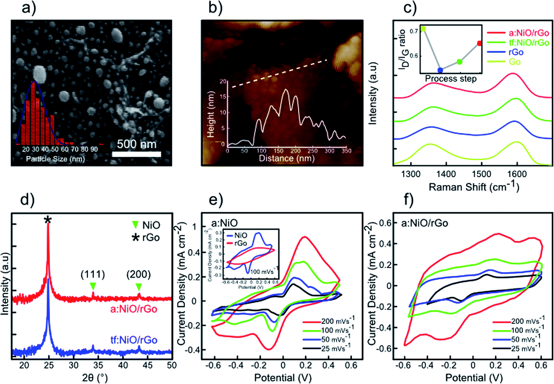 | ||
| Fig. 6 Characterization of a:NiO/rGO supercapacitor. (a) FESEM image of the annealed NiO film on rGO (a:NiO/rGO) with corresponding nanoparticle size distribution. (b) AFM image of a:NiO/rGO sample with height profile. (c) Raman evolution of D and G peaks of GO, rGO, tf:NiO/rGO, and a:NiO/rGO samples. Inset shows variation of ID/IG ratio in each step of NiO nanoparticles preparations. (d) XRD patterns of tf:NiO/rGO and a:NiO/rGO electrodes. (e) CV curves of a:NiO electrode at different scan rates and its comparison with rGO electrode (inset). (f) CV curves of a:NiO/rGO electrode at various scan rates. | ||
In the final analysis, the supercapacitor performance of the prepared a:NiO/rGO electrode is studied with the same method as the previous section. CV measurement of a:NiO/rGO electrode is performed at various scan rates with a potential window of 1.2 V as shown in Fig. 6f. Similar to the a:NiO/Si electrode, two redox peaks are observed in the CV curves due to oxidation/reduction reaction at the surface of the NiO nanoparticles.
Furthermore, as the scan rate increases, the position of the redox peaks shifts toward both ends as a result of internal resistance.48 However, the overall shape of the CV curves remains constant even at high scan rate, inferring a good rate capability of the a:NiO/rGO electrode.49 The highest measured capacitance was 4.80 mF cm−2 at the scan rate of 25 mV s−1, which is comparable with the values obtained for MoS2/rGO (3.74 mF cm−2) or a:NiO/Si (2.95 mF cm−2).
3.3. a:NiO/MoS2/rGO supercapacitor performance
In the previous section, supercapacitor based on rGO, MoS2, MoS2/rGO, and a:NiO/rGO electrodes were investigated by CV and GCD measurements. It was found that the MoS2/rGO electrode exhibited better capacitance performance compared to individual rGO and MoS2 electrodes. Besides, decoration of rGO with NiO nanoparticles revealed a remarkable enhancement in the capacitance capability (4.8 mF cm−2), comparable with all other fabricated electrodes. In addition, the MoS2/rGO electrode is further decorated with NiO nanoparticles. For this purpose, a 10 nm NiO film was sputtered on the MoS2/rGO hybrid structure using an RF sputtering unit. Then, thermal annealing was carried out for 30 min at 350 °C in the presence of argon ambient to convert the NiO film into the desired nanoparticles. Fig. 7a exhibits the SEM image of the a:NiO/MoS2/rGO electrode, in which the MoS2 and NiO nanoparticles are uniformly distributed over the rGO layers. Fig. 7b presents the CV curves of the a:NiO/MoS2/rGO electrode at various scan rates of 25, 50, 100, and 200 mV s−1 within the potential window between −0.6 V to +0.6 V. In all CV measurements, nearly symmetrical redox peaks are observed primarily due to surface redox reactions around NiO nanoparticles with rGO and MoS2 sheets.30,49 The same shape of high scan rate curves compared to low scan-rates indicates an excellent rate capacitance ability of the electrode. However, a slight shift can be observed in the position of the redox peaks due to the existence of internal resistance in the electrochemical process.48 A comparison between a:NiO/MoS2/rGO, a:NiO/rGO, and MoS2/rGO electrodes is shown in the inset of Fig. 7b for a similar scan-rate of 100 mV s−1. The dependence of areal capacitance on scan-rate is also presented in Fig. 7c for all fabricated electrodes. The tendency in reduction of areal capacitance with the increase in the scan rate is primarily due to the difficulty in ion transport at the electrode surface, which is observed for all presented electrodes.44 Fig. 7d shows the QCD measurement of the a:NiO/MoS2/rGO and a:NiO/rGO electrodes at the same current density of 0.2 mA cm−2. For a:NiO/rGO, a triangular shape of charge curve is observed, while the a:NiO/MoS2/rGO electrode possesses an asymmetric charge curve, which is attributed to the redox reaction related to the CV curves.48,49 At the current density of 0.2 mA cm−2, the longest discharging time of ∼34.5 s is achieved for a:NiO/MoS2/rGO, which is significantly higher than a:NiO/rGO (∼22 s), MoS2/rGO (∼18 s), rGO (∼8.7 s), and MoS2 (∼5.3 s) electrodes (inset of Fig. 7d).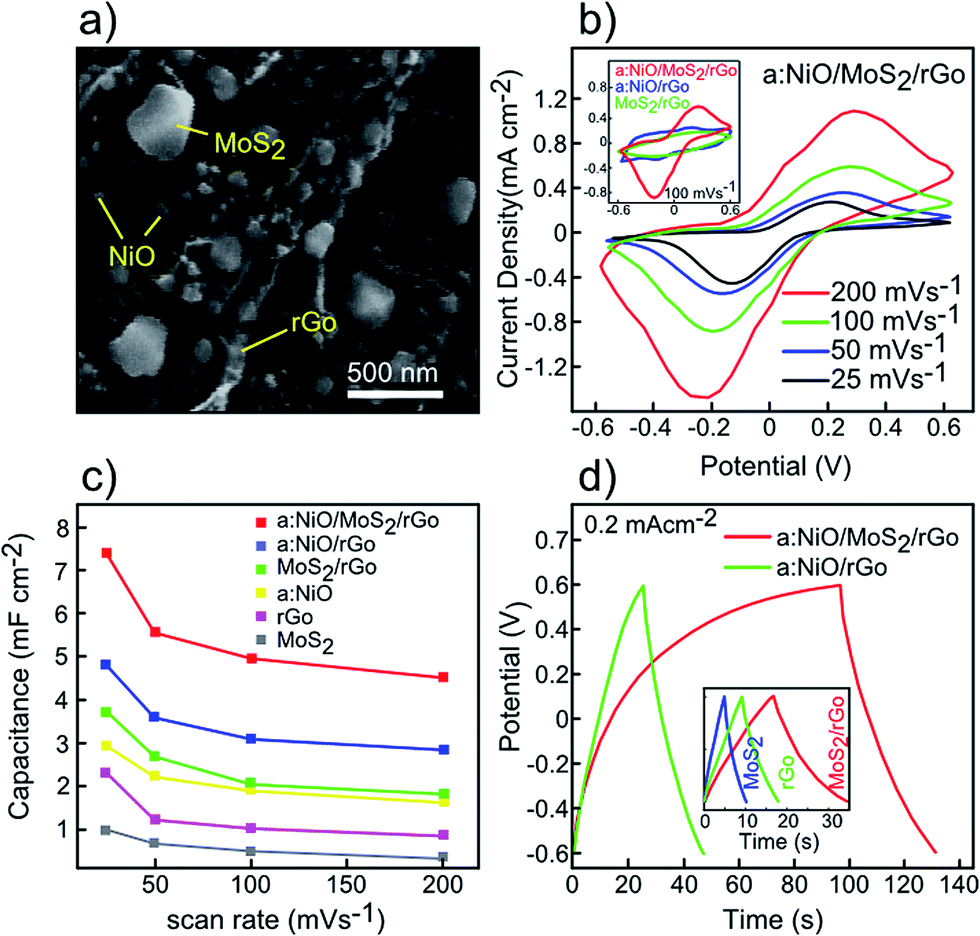 | ||
| Fig. 7 Supercapacitor performance of a:NiO/MoS2/rGO electrode. (a) FESEM image of the rGO–MoS2 electrode decorated with NiO nanoparticles. (b) CV curves of the a:NiO/MoS2/rGO electrode at various scan rates. Inset shows comparison of a:NiO/MoS2/rGO, a:NiO/rGO, and MoS2/rGO electrodes at same scan rate of 100 mV s−1. (c) Comparison of area capacitance of all fabricated electrodes as a function of scan rate. (d) GCD curves of a:NiO/MoS2/rGO and a:NiO/rGO electrodes at the current density of 0.2 mA cm−2. GCD curves of MoS2, rGO, and MoS2/rGO electrodes are shown in the inset at same current and potential window. | ||
During deposition of 10 nm NiO film, a slight increase in the active mass is expected. To investigate the effect of such mass increase on the final performance of electrodes, cyclic voltammograms of the fabricated electrodes are obtained. According to these measurements, gravimetric capacitance values of 156, 242, 320, and 562 F g−1 are obtained for rGO, MoS2/rGO, a:NiO, a:NiO/MoS2/rGO electrodes, respectively, at a scan rate of 25 mV s−1. Although the deposition of the NiO film leads to an increase in the electrode's active mass, the final capacitance of a:NiO/MoS2/rGO is still comparable with other presented electrodes.
The cycling stability of the a:NiO/MoS2/rGO electrode was also investigated using charging/discharging measurements at a current density of 0.2 mA cm−2 in the potential window of −0.6 V to +0.6 V over 1000 cycles (Fig. 8). It should be noted that only a few exemplary cycles have been plotted in this figure to show the near triangular charge–discharge characteristic of the electrode. Based on the results presented in Fig. 8, for the first 200 cycles, only 5% reduction in the initial area capacitance is observed; however, an additional charging/discharging process led to enhanced stability in capacitance, retaining approximately 90% of area capacitance after 1000-cycle test, which confirms a considerable cycling stability.
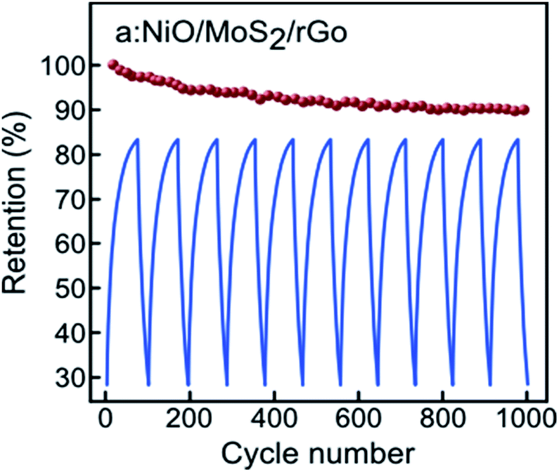 | ||
| Fig. 8 Cyclic stability of a:NiO/MoS2/rGO electrode at 0.2 mA cm−2 current density for 1000 cycles with corresponding selected QCD curves at potential window of 1.2 V. | ||
Based on all conducted CV measurements in the KCl electrolyte, rGO demonstrates the EDCL behaviour with rectangular CV curves, while MoS2 reveals quasi-rectangular CV shapes with weak redox peaks. Therefore, two distinctive charge storing mechanisms can be assigned to MoS2. In the non-faradic process, an electrical double layer is formed at the electrode/electrolyte interface by absorbing K+ ion:50
| (MoS2)surface + K+ + e− ↔ (MoS2–K+)surface | (1) |
Whereas in the redox process, H+ or K+ ions may diffuse into the MoS2 interlayers:50
| MoS2 + K+ + e− ↔ MoS–SK+ | (2) |
For the NiO nanoparticles, pseudocapacitive behaviour with two redox peaks is observed primarily due to absorption/desorption of K+ ions at the NiO surface resulting in partial charge-transfer over the electrode:51,52
| NiO + K+ + e−↔ (NiO–K+)surface | (3) |
It could be suggested that the EDLC behaviour of the MoS2 layer improves the capacitive performance of rGO, while its faradic behaviour does not significantly affect the final performance of the MoS2/rGO electrode. Creation of more active sites by faradic reaction at NiO surfaces as well as excellent charge transportation and mechanical stability of MoS2/rGO sheets result in a considerable enhancement of the final capacitance of the a:NiO/MoS2/rGO electrode.53–55
A comparison between selected fabricated supercapacitors from literature has been summarized in the Table 1. The reported values show that the NiO decorated capacitor (a:NiO/MoS2/rGO) possesses high area capacitance, which is even higher than the reported rGO–CNT electrodes.56 Indeed, rGO electrodes demonstrated an area capacitance in range of 0.5–3 mF cm−2, while MoS2 based supercapacitors exhibited 0.5–2 mF cm−2 capacitance.57–61 To enhance capacitance ability of MoS2 or rGO sheets, numerous attempts have been made in order to combine them with other relevant materials, such as SnO2, MnO2, and PANI polymer. However, the addition of these materials leads to unwanted side effects in the final devices.17,62,63 The data presented in this study suggest that the a:NiO/MoS2/rGO electrode can effectively store charge with high capacity and good cycling stability.
4. Conclusion
In this study, the capacitance capability of rGO, MoS2, and MoS2/rGO was investigated via a three-electrode electrochemical system. By thermal annealing of a 10 nm sputtered NiO film at 350 °C, rGO sheets were decorated with NiO nanoparticles with an average size of 35 nm, resulting in higher capacitance performance compared to rGO and MoS2/rGO samples. Moreover, a novel a:NiO/MoS2/rGO electrode was introduced with the highest area capacitance of ∼7.4 mF cm−2 at a scan rate of 25 mV s−1 along with the longest discharging time of ∼34.5 s at a current density of 0.2 mA cm−2, showing a remarkable improvement in comparison with other prepared electrodes. Although a pair of redox peaks were observed in the CV curves of the a:NiO/MoS2/rGO, the cycling test exhibited a good long term storage; about 90% of the initial capacitance was retained after 1000-cycle test. Therefore, our presented capacitor revealed an excellent capability in storing energy, making it an efficient device for energy consuming applications.Conflicts of interest
There are no conflicts to declare.Acknowledgements
Authors appreciate the Research Council of University of Tehran for partially funding this work. We are very thankful to Mrs Fatemeh Salehi for her strong support. We want also to acknowledge Mr Alireza Mashayekhi, Mr Morteza Hassan Pour, and Mr Naser Namdar for their kind scientific help.References
- D. Gielen, F. Boshell and D. Saygin, Nat. Mater., 2016, 15, 117–120 CrossRef CAS PubMed.
- S. Chu, Y. Cui and N. Liu, Nat. Mater., 2017, 16, 16–22 CrossRef PubMed.
- V. Dusastre and L. Martiradonna, Nat. Mater., 2017, 16, 15 CrossRef CAS PubMed.
- H. S. Jung and N.-G. Park, Small, 2015, 11, 10–25 CrossRef CAS PubMed.
- N. Mahato, A. Banerjee, A. Gupta, S. Omar and K. Balani, Prog. Mater. Sci., 2015, 72, 141–337 CrossRef CAS.
- X. Su, Q. Wu, J. Li, X. Xiao, A. Lott, W. Lu, B. W. Sheldon and J. Wu, Adv. Energy Mater., 2014, 4, 1300882 CrossRef.
- A. González, E. Goikolea, J. A. Barrena and R. Mysyk, Renewable Sustainable Energy Rev., 2016, 58, 1189–1206 CrossRef.
- J. Yan, Q. Wang, T. Wei and Z. Fan, Adv. Energy Mater., 2014, 4, 1300816 CrossRef.
- A. Borenstein, O. Hanna, R. Attias, S. Luski, T. Brousse and D. Aurbach, J. Mater. Chem. A, 2017, 5, 12653–12672 CAS.
- I. Shown, A. Ganguly, L.-C. Chen and K.-H. Chen, Energy Sci. Eng., 2015, 3, 2–26 CrossRef CAS.
- G. Zhang, X. Xiao, B. Li, P. Gu, H. Xue and H. Pang, J. Mater. Chem. A, 2017, 5, 8155–8186 CAS.
- Y. Zhang, L. Li, H. Su, W. Huang and X. Dong, J. Mater. Chem. A, 2015, 3, 43–59 CAS.
- R. Raccichini, A. Varzi, S. Passerini and B. Scrosati, Nat. Mater., 2015, 14, 271–279 CrossRef CAS PubMed.
- W. K. Chee, H. N. Lim, I. Harrison, K. F. Chong, Z. Zainal, C. H. Ng and N. M. Huang, Electrochim. Acta, 2015, 157, 88–94 CrossRef CAS.
- F. Bonaccorso, L. Colombo, G. Yu, M. Stoller, V. Tozzini, A. C. Ferrari, R. S. Ruoff and V. Pellegrini, Science, 2015, 347(6217), 1246501 CrossRef PubMed.
- Y. Ma, H. Chang, M. Zhang and Y. Chen, Adv. Mater., 2015, 27, 5296–5308 CrossRef CAS PubMed.
- H. Kashani, L. Chen, Y. Ito, J. Han, A. Hirata and M. Chen, Nano Energy, 2016, 19, 391–400 CrossRef CAS.
- X. Chia, A. Y. S. Eng, A. Ambrosi, S. M. Tan and M. Pumera, Chem. Rev., 2015, 115, 11941–11966 CrossRef CAS PubMed.
- R. Lv, J. A. Robinson, R. E. Schaak, D. Sun, Y. Sun, T. E. Mallouk and M. Terrones, Acc. Chem. Res., 2015, 48, 56–64 CrossRef CAS PubMed.
- D. Lembke, S. Bertolazzi and A. Kis, Acc. Chem. Res., 2015, 48, 100–110 CrossRef CAS PubMed.
- M. Acerce, D. Voiry and M. Chhowalla, Nat. Nanotechnol., 2015, 10, 313–318 CrossRef CAS PubMed.
- Y. Zhang, Y. Yu, L. Mi, H. Wang, Z. Zhu, Q. Wu, Y. Zhang and Y. Jiang, Small, 2016, 12, 1062–1071 CrossRef CAS PubMed.
- L. Niu, J. N. Coleman, H. Zhang, H. Shin, M. Chhowalla and Z. Zheng, Small, 2016, 12, 272–293 CrossRef CAS PubMed.
- J. Zheng, X. Yan, Z. Lu, H. Qiu, G. Xu, X. Zhou, P. Wang, X. Pan, K. Liu and L. Jiao, Adv. Mater., 2017, 29, 1604540 CrossRef PubMed.
- C. Backes, T. M. Higgins, A. Kelly, C. Boland, A. Harvey, D. Hanlon and J. N. Coleman, Chem. Mater., 2017, 29, 243–255 CrossRef CAS.
- F. Ghasemi and S. Mohajerzadeh, ACS Appl. Mater. Interfaces, 2016, 8, 31179–31191 CAS.
- F. Clerici, M. Fontana, S. Bianco, M. Serrapede, F. Perrucci, S. Ferrero, E. Tresso and A. Lamberti, ACS Appl. Mater. Interfaces, 2016, 8, 10459–10465 CAS.
- T. Audichon, T. W. Napporn, C. Canaff, C. Morais, C. Comminges and K. B. Kokoh, J. Phys. Chem. C, 2016, 120, 2562–2573 CAS.
- H. Yang, H. Xu, M. Li, L. Zhang, Y. Huang and X. Hu, ACS Appl. Mater. Interfaces, 2016, 8, 1774–1779 CAS.
- Y. Feng, H. Zhang, Y. Zhang, Y. Bai and Y. Wang, J. Mater. Chem. A, 2016, 4, 3267–3277 CAS.
- Z. Qiu, D. He, Y. Wang, X. Zhao, W. Zhao and H. Wu, RSC Adv., 2017, 7, 7843–7856 RSC.
- M. H. Amiri, N. Namdar, A. Mashayekhi, F. Ghasemi, Z. Sanaee and S. Mohajerzadeh, J. Nanopart. Res., 2016, 18, 1–14 CrossRef CAS.
- H. Tao, Y. Zhang, Y. Gao, Z. Sun, C. Yan and J. Texter, Phys. Chem. Chem. Phys., 2017, 19, 921–960 RSC.
- S. Sandoval, N. Kumar, J. Oro-Solé, A. Sundaresan, C. N. R. Rao, A. Fuertes and G. Tobias, Carbon, 2016, 96, 594–602 CrossRef CAS.
- W. L. Xu, C. Fang, F. Zhou, Z. Song, Q. Liu, R. Qiao and M. Yu, Nano Lett., 2017, 17, 2928–2933 CrossRef CAS PubMed.
- X. Chen, D. Meng, B. Wang, B.-W. Li, W. Li, C. W. Bielawski and R. S. Ruoff, Carbon, 2016, 101, 71–76 CrossRef CAS.
- C. K. Chua and M. Pumera, Chem. Soc. Rev., 2014, 43, 291–312 RSC.
- H. Huang, C. Lei, G. Luo, G. Li, X. Liang, S. Tang and Y. Du, Carbon, 2016, 107, 917–924 CrossRef CAS.
- X. Wang, I. Kholmanov, H. Chou and R. S. Ruoff, ACS Nano, 2015, 9, 8737–8743 CrossRef CAS PubMed.
- T. Kuila, A. K. Mishra, P. Khanra, N. H. Kim and J. H. Lee, Nanoscale, 2013, 5, 52–71 RSC.
- D. L. Matz, H. Sojoudi, S. Graham and J. E. Pemberton, J. Phys. Chem. Lett., 2015, 6, 964–969 CrossRef CAS PubMed.
- J. D. Renteria, S. Ramirez, H. Malekpour, B. Alonso, A. Centeno, A. Zurutuza, A. I. Cocemasov, D. L. Nika and A. A. Balandin, Adv. Funct. Mater., 2015, 25, 4664–4672 CrossRef CAS.
- Y. Hu, H. Cheng, F. Zhao, N. Chen, L. Jiang, Z. Feng and L. Qu, Nanoscale, 2014, 6, 6448–6451 RSC.
- X. Y. Liu, Y. Q. Gao and G. W. Yang, Nanoscale, 2016, 8, 4227–4235 RSC.
- N. Choudhary, M. Patel, Y.-H. Ho, N. B. Dahotre, W. Lee, J. Y. Hwang and W. Choi, J. Mater. Chem. A, 2015, 3, 24049–24054 CAS.
- D. Bouša, S. Huber, D. Sedmidubský, M. Pumera and Z. Sofer, Chem.–Eur. J., 2017, 23, 11961–11968 CrossRef PubMed.
- G. Zeng, W. Li, S. Ci, J. Jia and Z. Wen, Sci. Rep., 2016, 6, 36454 CrossRef CAS PubMed.
- Q. Li, Q. Wei, L. Xie, C. Chen, C. Lu, F.-Y. Su and P. Zhou, RSC Adv., 2016, 6, 46548–46557 RSC.
- L. Yu, G. Wan, X. Peng, Z. Dou, X. Li, K. Wang, S. Lin and G. Wang, RSC Adv., 2016, 6, 14199–14204 RSC.
- D. Li, D. Zhu, W. Zhou, Q. Zhou, T. Wang, G. Ye, L. Lv and J. Xu, J. Electroanal. Chem., 2017, 801, 345–353 CrossRef CAS.
- M.-S. Wu and C.-H. Yang, Appl. Phys. Lett., 2007, 91, 033109 CrossRef.
- H. Ma, J. He, D.-B. Xiong, J. Wu, Q. Li, V. Dravid and Y. Zhao, ACS Appl. Mater. Interfaces, 2016, 8, 1992–2000 CAS.
- B. Zhao, J. Song, P. Liu, W. Xu, T. Fang, Z. Jiao, H. Zhang and Y. Jiang, J. Mater. Chem., 2011, 21, 18792–18798 RSC.
- Y. Jiang, D. Chen, J. Song, Z. Jiao, Q. Ma, H. Zhang, L. Cheng, B. Zhao and Y. Chu, Electrochim. Acta, 2013, 91, 173–178 CrossRef CAS.
- L. Chen, Y. Yang, Y. Gao, N. Tronganh, F. Chen, M. Lu, Y. Jiang, Z. Jiao and B. Zhao, RSC Adv., 2016, 6, 99833–99841 RSC.
- J. Noh, C.-M. Yoon, Y. K. Kim and J. Jang, Carbon, 2017, 116, 470–478 CrossRef CAS.
- W. Gao, N. Singh, L. Song, Z. Liu, A. L. M. Reddy, L. Ci, R. Vajtai, Q. Zhang, B. Wei and P. M. Ajayan, Nat. Nanotechnol., 2011, 6, 496–500 CrossRef CAS PubMed.
- M. Beidaghi and C. Wang, Adv. Funct. Mater., 2012, 22, 4501–4510 CrossRef CAS.
- H. Wang, Z. Lu, D. Kong, J. Sun, T. M. Hymel and Y. Cui, ACS Nano, 2014, 8, 4940–4947 CrossRef CAS PubMed.
- A. Winchester, S. Ghosh, S. Feng, A. L. Elias, T. Mallouk, M. Terrones and S. Talapatra, ACS Appl. Mater. Interfaces, 2014, 6, 2125–2130 CAS.
- C. Fenglian, T. Cheng-an, L. Yujiao, Y. Wenchang, W. Xueye and W. Jianfang, Mater. Res. Express, 2017, 4, 036304 CrossRef.
- Y. Zhang and Y. Zhai, RSC Adv., 2016, 6, 1750–1759 RSC.
- A. Maizelis and B. Bairachniy, Nanoscale Res. Lett., 2017, 12, 119 CrossRef PubMed.
- J. Lin, C. Zhang, Z. Yan, Y. Zhu, Z. Peng, R. H. Hauge, D. Natelson and J. M. Tour, Nano Lett., 2013, 13, 72–78 CrossRef CAS PubMed.
| This journal is © The Royal Society of Chemistry 2017 |