
 Open Access Article
 This Open Access Article is licensed under a
 Creative Commons Attribution 3.0 Unported Licence
A highly efficient quantum dot light emitting diode via improving the carrier balance by modulating the hole transport
Jiangyong Pan,
Jing Chen *,
Qianqian Huang,
Lixi Wang and
Wei Lei*
*,
Qianqian Huang,
Lixi Wang and
Wei Lei*
Joint International Research Laboratory of Information Display and Visualization, School of Electronic Science and Engineering, Southeast University, Nanjing, 210096, China. E-mail: chenjing@seu.edu.cn
First published on 7th September 2017
Abstract
A high-performance solution processed quantum dot light emitting diode (QLED) has been fabricated via modulating the hole transport by doping 1-bis[4-[N,N-di(4-tolyl)amino]phenyl]-cyclohexane (TAPC) into poly-N-vinylcarbazole (PVK) as the hole transport layer (HTL). With a low doping content, the hole transport ability of the HTL can be enhanced due to the extremely high hole mobility of TAPC. However, increasing the doping ratio of TAPC excessively results in degraded performance of the QLED due to the deteriorated film quality and increased energy barrier from the HTL to the quantum dots (QDs), which is attributed to the relatively shallow position of the HOMO level for TAPC. Using the optimized composition ratio of the doped HTL (3![[thin space (1/6-em)]](https://www.rsc.org/images/entities/char_2009.gif) :1 vol% of PVK:TAPC), the best QLED performance was achieved with a low turn-on voltage of 3.3 V due to the charge balance, which facilitates exciton recombination in the emissive layer (EML). In addition, the highest current efficiency (26.2 cd A−1), power efficiency (19.2 lm W−1), external quantum efficiency (6.2%) and 60% enhancement in the stability of the device were achieved. The improvement in the device performance can be attributed to the suppression of Auger recombination due to the balance of carrier injection into the emissive layer composed of QDs and the separation of the carrier accumulation zone from the exciton formation interface by the modulation of hole transport. The lowered turn-on voltage and improved efficiency presented here offer potential for high throughput and practical use for commercialized QLED displays.
:1 vol% of PVK:TAPC), the best QLED performance was achieved with a low turn-on voltage of 3.3 V due to the charge balance, which facilitates exciton recombination in the emissive layer (EML). In addition, the highest current efficiency (26.2 cd A−1), power efficiency (19.2 lm W−1), external quantum efficiency (6.2%) and 60% enhancement in the stability of the device were achieved. The improvement in the device performance can be attributed to the suppression of Auger recombination due to the balance of carrier injection into the emissive layer composed of QDs and the separation of the carrier accumulation zone from the exciton formation interface by the modulation of hole transport. The lowered turn-on voltage and improved efficiency presented here offer potential for high throughput and practical use for commercialized QLED displays.
Introduction
Recently, quantum dots (QDs) have gained significant attention because of their superior characteristics, such as broad wavelength tunability over the entire visible spectrum due to their size dependence, high color purity, and solution-processability.1–11 QDs have been actively investigated for use in optoelectronic devices ranging from down-converters in backlit displays, light-emitting diodes (LEDs), lasers, and photo-detectors to solar cells.12–16 Among these potential applications, the realization of high-performance quantum dot light emitting diodes (QLEDs) has been recognized as a promising research field due to their potentially immediate and significant impact in display and lighting technologies. Since the first report of colloidal QLEDs,12 many approaches have been conducted to improve the device performance including the modification of the structure and synthesis of high quality materials. For example, Dai et al. have reported high-performance QLED by inserting an insulating layer between the QD layer and the oxide electron transport layer to optimize charge balance in the device and preserve the superior emissive properties of the QDs.17 In addition, Yang et al. have demonstrated the QLED with the fine nanostructure of QDs especially the composition of the graded intermediate shell and the thickness of the outer shell, which plays a very important role in determining QLED performance due to its effect on charge injection, transport and recombination.18A main obstacle towards improving QLED performance is intrinsic processes in the device, such as multicarrier Auger recombination or electron–hole separation due to applied electric field. Here we tried to solve the problem of Auger recombination, which impacts both QLED efficiency and the onset of efficiency roll-off at high currents.19 It has been found that the Auger recombination is attributed to charging of QDs with extra electrons due to the imbalance of charge transport.20 It is prone to the imbalance of charge in the conventional QLEDs due to the characteristic band structure of the component layers. The valence band (VB) (∼−6 eV to −7 eV) of QDs is usually much lower than the highest occupied molecular orbital (HOMO) of typical conjugated organic molecules or polymers, which are usually utilized as the hole transport layer (HTL), and the conduction band (CB) (∼−4 eV) is similar to that of metal oxide acting as the electron transport layer (ETL),21,22 thus the energy band of the QD is much more beneficial for electron injection than for hole injection, resulting in the imbalance of carrier transportation. Generally, the single layer of poly-N-vinylcarbazole (PVK) has been widely used as an HTL for QLEDs in the past two years.23 Compared with the other HTL materials, the HOMO level of PVK is rather low (∼−5.8 eV), but the hole mobility is quite small (2.5 × 10⁻⁶ cm2 V−1 s−1), which restricts the hole transport.24 Therefore, it is highly desirable to dope the HTL materials to modulate the hole transport in order to balance the carrier transport, leading to improvement in the QLEDs performance.
Recently, it has been attempted to adopt the hybrid HTL, which takes advantage of both deep HOMO level and high hole mobility of the components within the hybrid HTL. For instance, a proper blending ratio of poly-N-vinylcarbazole (PVK) and 4,4′,4′′-tris(N-carbazolyl)-triphenyl-amine (TCTA) has been utilized as the HTL in the QLEDs,25 as well as the blending of poly(4-butyl-phenyl-diphenyl-amine) (poly-TPD) and TCTA as the HTL reported by another group.26 However, the hole mobility of the blending material of TCTA is fairly low (2.0 × 10⁻⁵ cm2 V−1 s−1),27 which weakens the effect of band level adjustment and influences the hole transport. In addition, our group has tried to blend 4,4′-bis-(carbazole-9-yl)biphenyl (CBP) with PVK to function as the hybrid HTL. Although the performance of the optimized device was improved, it is still far away from the anticipated performance, which is primarily due to the poor film quality caused by the relatively low glass transition temperature (Tg of ∼62 °C) of CBP.28
Herein, we demonstrate highly improved performance of QLEDs by using PVK doped with 1-bis[4-[N,N-di(4-tolyl)amino]phenyl]-cyclohexane (TAPC), which has been used in the tandem OLED.29 The capability of hole transport in the blended HTL is modulated and enhanced by taking the advantages of high hole mobility of TAPC (1.0 × 10⁻² cm2 V−1 s−1) in the OLED27 and superior energy level of PVK, leading to promoted balance of charge carrier injection and transport. The current efficiency, power efficiency and EQE increased to 26.2 cd A−1 and 19.2 lm W−1 and 6.2%, respectively. The mechanism of the improvement in the device performance will be discussed.
Experimental procedure
Quantum dots synthesis
The green emitting CdSe/ZnS QDs were synthesized according to the modified method reported previously.10 Here, 0.4 mmol of CdO, 4 mmol of zinc acetate, 4 mmol of oleic acid (OA), and 20 mL of 1-octadecene were mixed in a 100 mL round flask. The mixture was heated to 150 °C degassed for 30 min under ∼10 Pa pressure, filled with high-purity N2 flow. Next, the whole system was further heated to 300 °C to form a clear solution of Cd(OA)2 and Zn(OA)2. At this temperature, a stock solution containing 3 mL of trioctylphosphine, 0.4 mmol of Se, and 4 mmol of S was quickly injected into the reaction flask. After the injection, the reaction temperature was maintained for 10 min. The reaction was subsequently cooled down to room temperature to stop further growth. The QDs were washed with acetone three times, and finally dispersed in hexane at a concentration of 10 mg mL−1.ZnO nanoparticles synthesis
The ZnO NPs were synthesized by blending a solution of 0.5 M tetramethylammonium hydroxide (TMAH) in ethanol with 0.1 M zinc acetate in dimethyl sulfoxide (DMSO). Next, the blending solution was stirred for 1 hour in ambient conditions. The prepared product was collected and then washed with acetone a few times. The obtained transparent precipitate was dispersed in butanol with a concentration of 30 mg mL−1.Preparation of doped HTL
The doping of HTL was prepared by mixing PVK (10 mg mL−1) and TAPC (5 mg mL−1) in a chlorobenzene solution with a ratio of 5:1, 4:1, 3:1, 2:1 and 1:1 by volume, respectively.
Fabrication of QLED device
QLEDs were fabricated on ITO-coated glass, which was carefully cleaned with de-ionized water, acetone and iso-propanol, consecutively, and then treated with ozone generated by ultraviolet light for 30 min. Poly(ethylenedioxythiophene):polystyrenesulfonate (PEDOT:PSS) solutions were spin-coated onto the ITO glass substrates after filtering as the hole injection layer (HIL) and baked at 140 °C for 15 min under ambient conditions. Then, the PEDOT:PSS-coated substrates were transferred into a glovebox (O2 < 0.1 ppm, H2O < 0.1 ppm) for spin-coating the other layers. The doped HTL was spin-coated and annealed at 120 °C for 20 min, which was followed by the spin-coating of the QDs (10 mg mL−1 in hexane) layered as the emissive layer (EML) at 1500 rpm for 30 s. Next, the ZnO NPs (30 mg mL−1 in butanol) were spin-coated as the electron transport layer (ETL) at 4000 rpm for 30 s. Finally, the layers-coated substrates were transferred to the custom high-vacuum deposition chamber (background pressure, 6 × 10⁻⁴ torr) to deposit the aluminum as the electrode. The control device with pristine PVK as the HTL was also fabricated according to the method mentioned above for comparison.Characterizations
The absorption and photoluminescence spectra were measured using a UV-visible instrument (U-4100). Transmission electron microscopic (TEM) measurement was performed using a Tecnai G2 F20 operating at 200 kV. Atomic force microscopy (AFM) was measured with Veeco Dimension 3100 at ambient temperature in tapping mode. EL spectra and luminance–current density–voltage characteristics of QLEDs were obtained with a Minolta luminance meter (LS-100) coupled with a Keithley 2400 voltage and current source under ambient conditions.Results and discussion
Core/shell CdSe/ZnS QDs were used in the QLED device as the emissive layer. As shown in Fig. 1(a), the characteristic exciton absorption peak of QDs is located at 520 nm, while the PL spectrum exhibiting a Gaussian profile has a maximum emission located at 530 nm. There are no defect emissions observed, indicating an efficient exciton recombination and confinement in the CdSe core. It was also found that the QDs were uniformly dispersed in the solvent with an average diameter of approximately 6 nm. The structure of the QLED device is displayed in Fig. 1(b). The multilayer QLED device is composed of ITO/PEDOT:PSS/doped HTL/QDs/ZnO/Al, where PEDOT:PSS is used as the HIL, PVK:TAPC as the doped HTL, CdSe/ZnS QDs as the emissive layer (EML), and ZnO NPs as the ETL. Here, TAPC is introduced into the HTL to form the doped HTL to facilitate the hole transport due to its high hole mobility. Which is attributed to the un-bonded electrons of nitrogen coupled with the floating electrons of benzene ring to form the large π-ring. Though the Tg of TAPC increases to 78 °C owing to the introduction of the bulky cyclohexane ring shown in Fig. 1(c),30 it is relatively lower compared with the Tg of other small molecule HTL materials, such as TCTA (151 °C).31 The relatively low Tg will damage the film quality fabricated by spin-coating, thus the ratio of TAPC in the doped HTL should be optimized. For the ETL, ZnO can be a good candidate due to its superior energy band of conduction band (CB) of 4.3 eV and valence band (VB) of 7.4 eV,32 which results in the small conduction band offset and large valence band offset at the QD/ZnO NPs. Thus, the ZnO NPs layer not only facilitate efficient electron injection from the Al cathode into the QDs but also prevents the leakage of holes to the adjacent ZnO NPs layer, which is in favor of confining the excitation–recombination region, thereby improving the charge recombination efficiency.
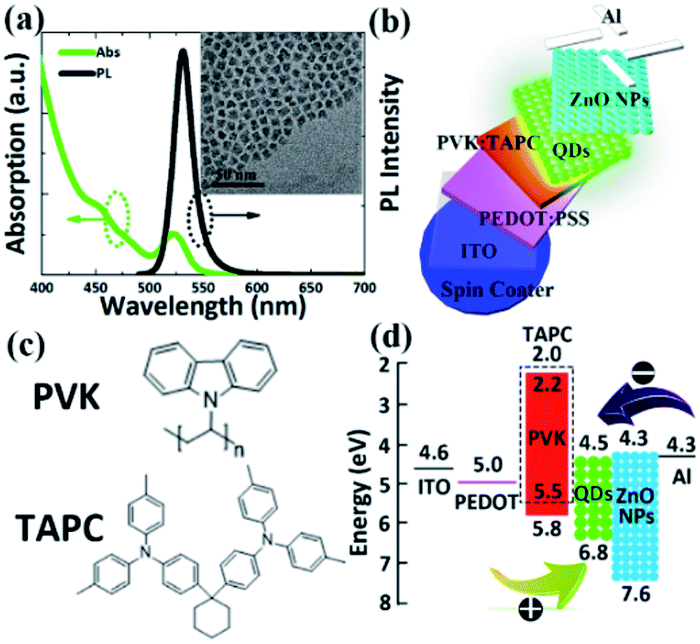 | ||
| Fig. 1 (a) The absorption and PL spectra of the QDs. Inset shows the TEM image of QDs. (b) Device schematic of multilayered QLED. (c) Molecular structure of the HTL materials of PVK and TAPC. (d) Energy diagram of the prepared QLED. | ||
The characteristics of prepared ZnO have been studied further as displayed in Fig. 2. The ZnO NPs have the diameter of approximately 3.5 nm with the absorbance peak of 325 nm and PL peak of 545 nm. It can also be verified from the XRD pattern that our synthesized ZnO NPs have a wurtzite structure as shown in Fig. 2(c). In addition, the high electron mobility of ZnO has been measured to be 4 × 10⁻³ cm2 V−1 s−1 based on the TFT transfer characteristics of ZnO NP film as displayed in Fig. 2(d), which also makes ZnO a good candidate for the ETL. It is found that the holes are restricted due to the relatively low hole mobility of PVK and larger barriers (1.0 eV) at the interface of the HTL/EML compared with that of ETL/EML in the conventional QLED. The imbalance of carrier injection leads to the accumulation of excess electrons in the EML, which consequently enhances the non-radiative Auger assisted recombination or leak to the counter electrode without recombination, thus greatly reducing the efficiency and stability of the devices.20 Therefore, it is necessary to balance the electron and hole currents by promoting the hole transport. TAPC was introduced into PVK to form the doped HTL, taking its fairly high hole mobility into account.
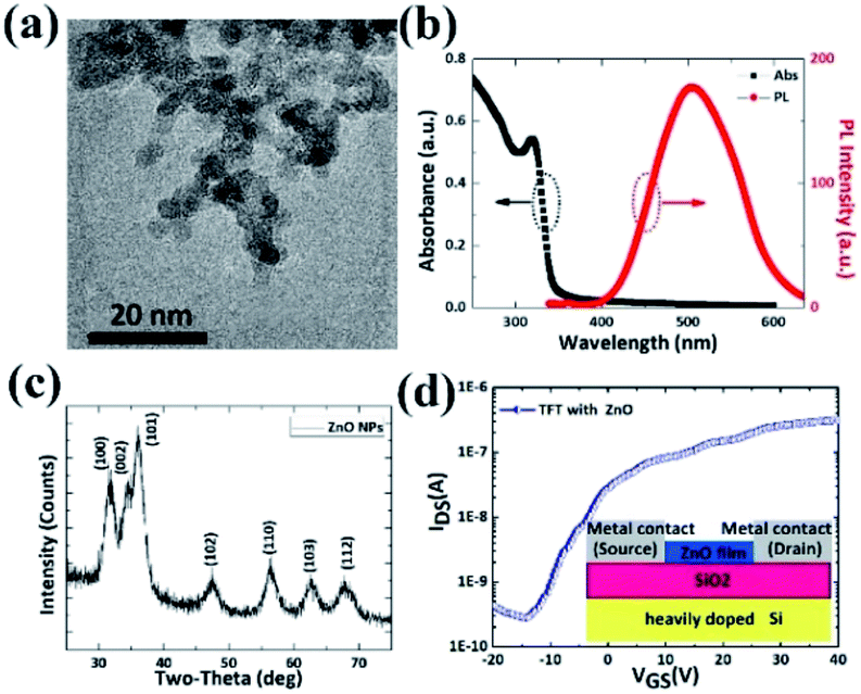 | ||
| Fig. 2 (a) The TEM image, (b) the absorption and PL spectra and (c) XRD image of ZnO NPs. (d) TFT transfer characteristics of ZnO nanoparticle film. | ||
For multilayer QLED devices, the surface roughness of underlayer have great effects on the uniformity of following deposited top layer, further influencing the device performance due to the usage of spin-coating technique.33 For this study, the QDs layer was spin-coated on the HTL layer, therefore the roughness of the HTL layer plays an important role in the film quality of the QDs deposition. As shown in Fig. 3 and Table 1, the bare PVK film coated on the PEDOT:PSS has the smallest roughness of root mean square (Rq) of 0.57 nm, while doping TAPC into PVK degrades the uniformity of the film due to the relatively low Tg of TAPC. In addition, it is worth noting that the uniformity of the film will deteriorate when the blend ratio of PVK exceeds 2:1.
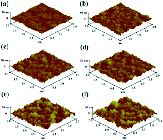 | ||
| Fig. 3 AFM image of different doped HTL coated on the PEDOT:PSS layer (a) PVK (b) PVK:TAPC = 5:1 (c) PVK:TAPC = 4:1 (d) PVK:TAPC = 3:1 (e) PVK:TAPC = 2:1 (f) PVK:TAPC = 1:1. | ||
| The volume ratio of PVK and TAPC | ||||||
|---|---|---|---|---|---|---|
| PVK | 5:1 |
4:1 |
3:1 |
2:1 |
1:1 |
|
| Rpv (nm) | 4.33 | 5.57 | 5.84 | 6.37 | 7.42 | 10.9 |
| Rq (nm) | 0.57 | 0.71 | 0.73 | 0.93 | 1.13 | 3.1 |
| Ra (nm) | 0.45 | 0.56 | 0.58 | 0.78 | 1.01 | 2.25 |
The change of the energy band of the doped HTL should be evaluated seriously because of the difference of the energy band structure between these two HTL materials. Thus, the energy levels of doped HTL has been confirmed by the ultraviolet photoelectron spectroscopy (UPS) measurements. The resulting secondary-electron cutoff and valence-band regions are shown in Fig. 4(a) and (b), respectively. Generally, the work function (WF) could be estimated by the difference between the incident light energy (21.2 eV) and the energy of secondary cutoff.34 In this case, the PVK and PVK:TAPC films are calculated to be 4.75 eV and 4.65 eV, respectively, as labeled in Fig. 4(a). In order to define the position of valence band maximum (VBM), the energy gap between Fermi level and VBM (ΔEVB) is extracted from the valence-band region. As shown in Fig. 3(b), the ΔEVB values of PVK and PVK:TAPC are 1.05 eV and 1.10 eV, respectively. As a result, via the summation of WF and ΔEVB, the VBM levels of PVK and PVK:TAPC films are calculated to be 5.80 eV and 5.75 eV below the vacuum level, respectively. Fig. 3(d) shows the absorption spectra of PVK and PVK:TAPC, which is converted from Fig. 3(c). The band gaps (Eg) of these two materials could be determined through the absorption onset of the linear region and the Eg values for PVK and PVK:TAPC are found to be 3.64 eV and 3.72 eV, respectively. Therefore, the conduction band minimum (CBM) levels are deduced to be 2.16 eV for PVK and 2.03 eV for PVK:TAPC. It is noted that the HOMO remains nearly unchanged at this blending ratio of PVK to TAPC at 3:1, which slightly influences the hole transport.
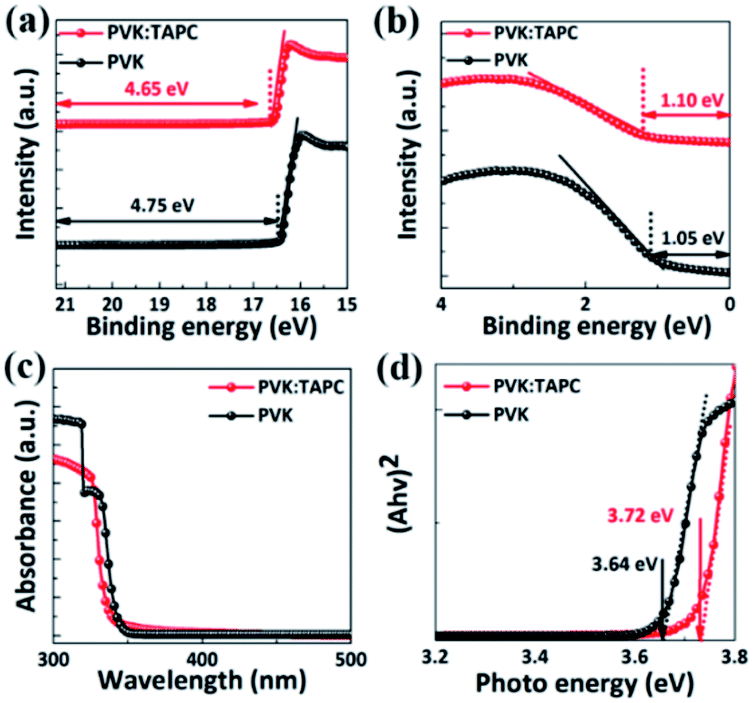 | ||
| Fig. 4 UPS spectra of (a) the secondary cut off region and (b) the HOMO region, (c) absorption spectra, (d) (Ahν)2–hν plots of HTL converted from (a) of PVK and PVK blending TAPC films (blending ratio is 3:1). | ||
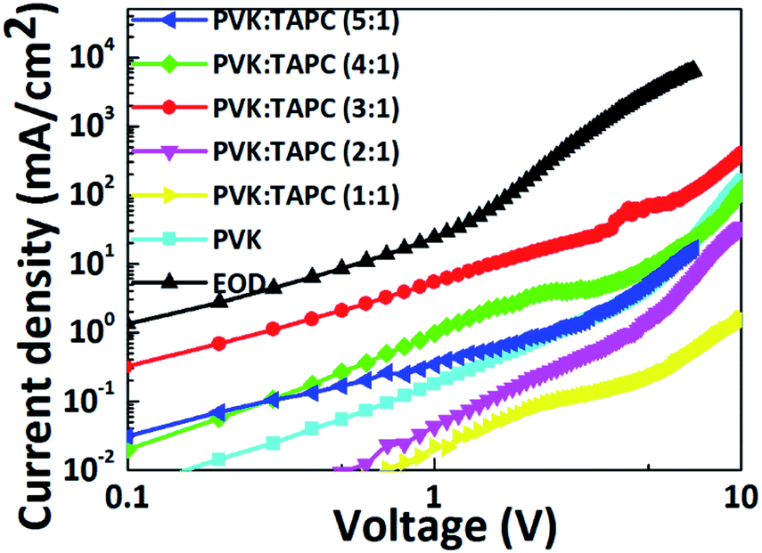
To verify the effect of doping TAPC into PVK on the carrier transport, the electron-only device (EOD) (ITO/ZnO/QDs/ZnO/Al) and hole-only device (HOD) (ITO/PEDOT:PSS/HTL/QDs/MoO3/Al) were fabricated. It should be mentioned that the thicknesses of all layers in the above charge-only devices are identical to those used in the working devices. It can be easily found that the current of EOD is much larger than that of HOD with bare PVK as displayed in Fig. 5, because the ZnO NPs are in favor of electron transport due to its similar LUMO level with the CB of QDs (Fig. 1(d)). In contrast, the holes are restricted due to the low hole mobility and shallow HOMO level of PVK, which results in the imbalance of carrier transport. It is anticipated that doping appropriate amount of TAPC into the PVK leads to the high hole mobility. It is clearly reflected in Fig. 5 that the current density of HOD increases with the increased amount of TAPC in PVK and reaches the highest and closest value to the current of EOD when the doping ratio of PVK:TAPC is 3:1. However, when the doping concentration of TAPC increases, the hole transport can be restricted because the film quality will deteriorate as discussed above and the HOMO will decrease due to the comparatively smaller HOMO of TAPC. Thus, it can be speculated that the QLED device with PVK:TAPC (3:1) has the best performance upon the balance of carrier transport attributed to the high hole mobility and appropriate HOMO level of the doped HTL.
 | ||
| Fig. 5 Current–voltage characteristics of the EOD (ITO/ZnO/QD/ZnO/Al) and HODs (ITO/PEDOT:PSS/HTL/QD/MoO3/Al). | ||
To further verify the effect of doped HTL, QLED devices with different ratios of PVK and TAPC were fabricated. Fig. 6(a) shows higher luminance of QLED with PVK:TAPC (3:1) as doped HTL, indicating the carrier transport is balanced at this condition and it is in favor of the radiative recombination in the EML. At the same time, the HOMO of the doped HTL remains nearly unchanged compared with the bare PVK, which facilitates the hole transport. It is displayed in Fig. 6(a) that both the turn on voltage (3.3 V) of QLED with PVK:TAPC (3:1) as doped HTL and the driving voltage at the highest current efficiency (∼4 V) are lower compared with those (∼6 V and ∼8 V) demonstrated by the other group.35 It is attributed to the carrier balance at this condition due to the enhanced hole transport ability when using the doped HTL, which facilitate the exciton recombination in the EML. In addition, it can be found that the QLEDs with TAPC:PVK = 3:1 show the highest current efficiency and power efficiency of 26.2 cd A−1 and 19.2 lm W−1, i.e. an increase by 55% and 51%, respectively, compared to the device with pristine PVK. It is noted that the efficiencies of the device exceed those of the similar device in the previous work published.25,26 This is because the hole mobility of small molecule used here (TAPC: 1.0 × 10⁻² cm2 V−1 s−1) is much higher than that of the small molecule used in other work (TCTA: 2.0 × 10⁻⁵ cm2 V−1 s−1). Moreover, the doping ratio of doped HTL has been adjusted carefully to facilitate hole transport and ensure the film quality of the HTL layer, which plays an important role in the film quality of the QDs deposition. All these factors contribute to the performance improvement of QLEDs. In addition, the external quantum efficiency (EQE) of the QLED with PVK:TAPC (3:1) as doped HTL reaches the highest value of 6.2% because of the balanced carrier transport due to the improvement in hole transport ability as displayed in Fig. 6(c). It is worth noting that efficiencies close to the peak value (i.e. EQE ≥90% EQE peak) are maintained in a wide range of brightness of 500–22000 cd m−2. The low efficiency roll-off of this device suggests that our QLEDs are promising for high-power applications. A summary of the QLEDs performance with different HTLs is displayed in Table 2. It is worth noting that when the ratio of PVK and TAPC decreases further, such as 1:1, the performance of the QLED will experience a fast roll-off of efficiency. This is because the film quality will deteriorate when the doping concentration of TAPC is larger due to the relatively low Tg of TAPC as displayed in Fig. 3. Another reason is likely that the HOMO of the doped HTL will become shallower as the doping concentration of TAPC increases excessively, attributing to the small HOMO level of TAPC. Therefore, the performance improvement of the QLED device is attributed to the balance of carrier transport when utilizing the doped HTL, which takes advantage of the superior energy level of PVK and high hole mobility of TAPC. In order to make the conclusion more reliable, a comparison of the average current efficiency of QLEDs with respect to TAPC doping is displayed in Fig. 6(d), considering the device-to-device performance variations. It clearly shows the same variation trend as the single device. In addition, an encouraging high reproducibility of this high performance of our QLEDs was demonstrated by testing 36 devices from 8 batches as shown by the histograms in Fig. 6(e), yielding an average efficiency of 24.1 cd A−1. Electroluminescence (EL) of the device with PVK:TAPC (3:1) as doped HTL at different driving voltage is shown in Fig. 6(f), exhibiting the same EL peak wavelength without peaks from neighbouring organic layers. This demonstrates that the excitons effectively recombine in the QDs layer. The luminescence intensity greatly increases with the increased driving voltage and the device emits the vivid light as shown in the inset of Fig. 6(f). Compared with the PL spectrum, the peak location of the EL spectrum is slightly red-shifted (∼10 nm), which is due to enhanced interdot interactions resulting from the reduced interdot distance in close-packed QDs film, electric-field-induced Stark effect and long-range resonance transfer of electronic excitations from the small to the large dots.36
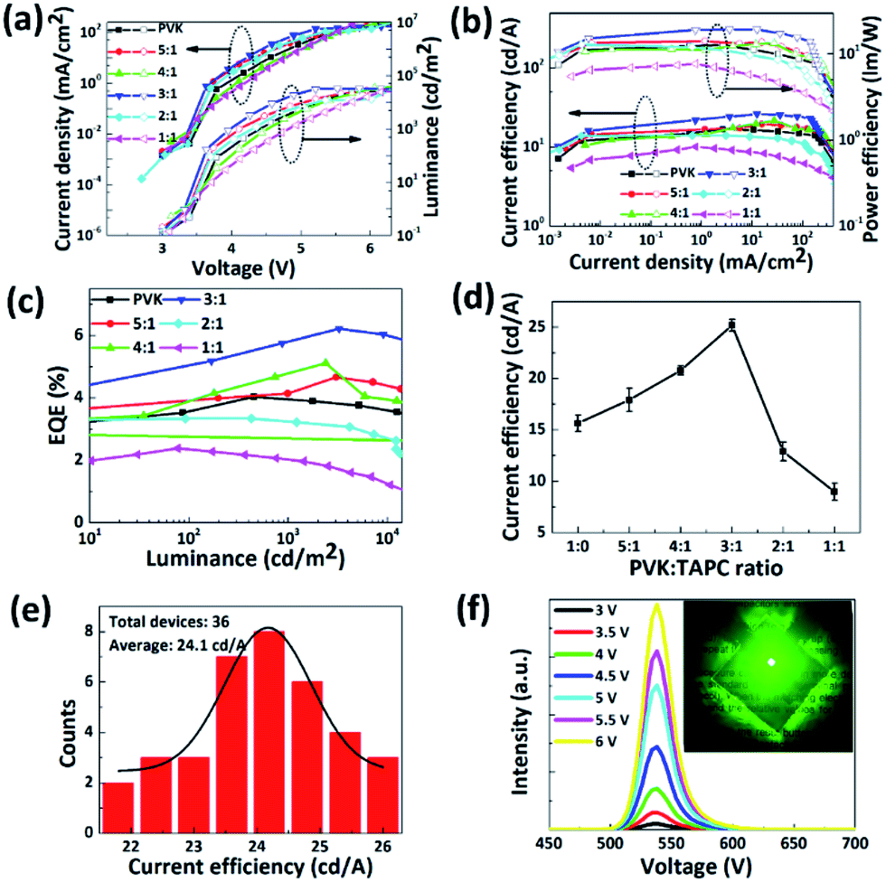 | ||
| Fig. 6 (a) Current-density–luminance–voltage (J–L–V) characteristics, (b) current efficiency and power efficiency characteristics, (c) EQE characteristics of QLEDs with different HTL (d) comparison of the average current efficiency as a function of TAPC doping ratio. Each data point is averaged over 8 devices per data point with the error bars. (e) Histogram of current efficiencies of 36 devices for green QLEDs, and (f) EL spectra of sample QLED with PVK:TAPC (3:1), inset shows luminance photos of QLED device. | ||
| Device | VT | VD | EQE (%) | CE (cd A−1) | PE (lm W−1) | ||
|---|---|---|---|---|---|---|---|
| Peak | @1000 cd m−2 | Peak | @1000 cd m−2 | ||||
| a VT driving voltage corresponding to 1 cd m−2, VD driving voltage corresponding to 1000 cd m−2. | |||||||
| PVK | 3.5 | 4.4 | 4.0 | 16.9 | 16.5 | 12.7 | 11.8 |
| PVK:TAPC (5:1) |
3.4 | 4.5 | 4.6 | 19.4 | 17.3 | 13.6 | 13.3 |
| PVK:TAPC (4:1) |
3.3 | 4.5 | 5.1 | 21.6 | 18.2 | 13.3 | 12.8 |
| PVK:TAPC (3:1) |
3.3 | 4.0 | 6.2 | 26.2 | 24.8 | 19.2 | 19.0 |
| PVK:TAPC (2:1) |
3.5 | 4.3 | 3.5 | 14.1 | 13.7 | 12.9 | 10.2 |
| PVK:TAPC (1:1) |
3.4 | 4.8 | 2.4 | 10.1 | 8.5 | 7.7 | 5.4 |
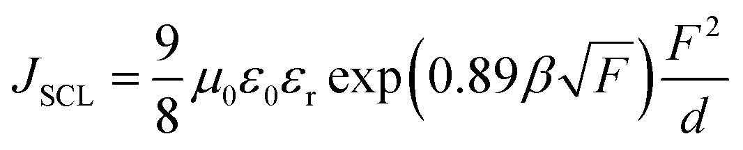
In order to further verify the conclusion that device performance improved is attributed to carrier balance, the same method widely used in OLED is adopted to calculate the injection efficiency of hole in our devices. At first, devices with a structure of ITO/PEDOT:PSS/HTL/Au were fabricated to test the hole injection enhancement of the doped HTL device. It is noted that Au was used as cathode here to ensure only the hole transport in these devices. It is found that the device exhibited a great enhancement of current density when the doping ratio of PVK:TAPC is 3:1 as displayed in Fig. 7(a). For instance, the device with the PVK:TAPC (3:1) as doped HTL shows a current density of 10 mA cm−2, larger than that of any other types of devices. The theoretical SCLC displayed in Fig. 7(a) is the calculated current density. Ideally, if an organic material is under condition of ohmic injection contact as well as trap-free, the steady-state current should follow the space-charge-limited current (SCLC) (JSCL):37
 | (1) |
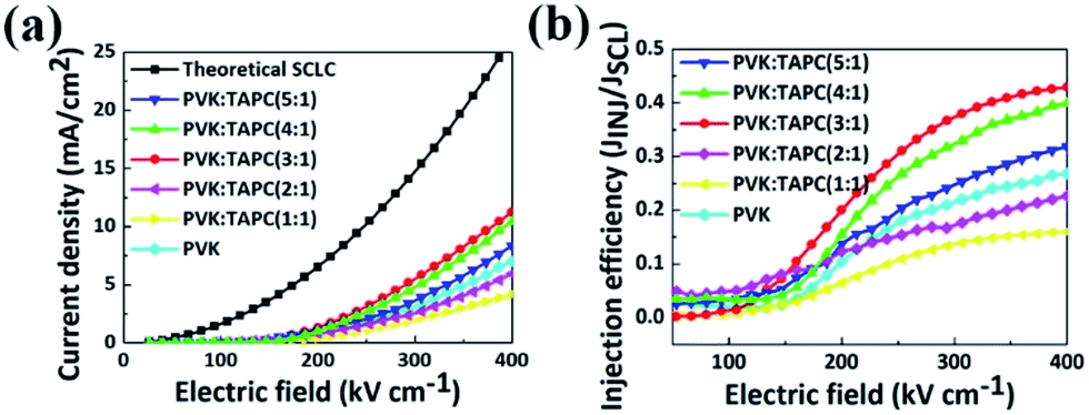 | ||
| Fig. 7 (a) J–V characteristics, and (b) hole injection efficiency, ηINJ, of hole-only device as a function of electric field of devices with different HTL. | ||
The injection efficiency ηINJ can be calculated from the J–V characteristics:40
| ηINJ = JINJ/JSCL | (2) |
The hole injection efficiency (ηINJ) curves of different HTL devices is displayed in Fig. 7(b) according to the formula (1) and (2). It can be easily found that the ηINJ increases from 13.2% of the device with PVK as HTL to 40.1%, when adopting the PVK:TAPC (3:1) as doped HTL. Thus, a significant improvement of hole injection efficiency can be obtained using the PVK:TAPC (3:1) as doped HTL, which facilitates the charge balance as well as high performance QLED.
The QLED utilizing the optimized doped HTL exhibits better ambient stability without any encapsulation techniques compared with that with the pristine HTL. For the fair comparison of device lifetime, the constant current of 39 mA cm−2 was applied for the two devices. The device lifetime is estimated by the relation of L0n × T50 = constant (1.5 ≤ n ≤ 2).17 L0 is the initial luminance, 3900 cd m−2 and 4900 cd m−2 for the device with pristine HTL and device with doped HTL and device with doped HTL, respectively. T50 (defined as the time for the luminance reducing to L0/2) is about 9 h and 14 h respectively for the two devices according to Fig. 8. The values of acceleration factor n was assumed as 1.5 according to the literature.17 The device lifetime at initial luminance of 100 cd m−2, calculated by the relation above, is over 2400 and 4000 h for devices with pristine HTL and device with doped HTL, respectively. An enhancement factor of 60% is obtained for the device lifetime when doped HTL is introduced.
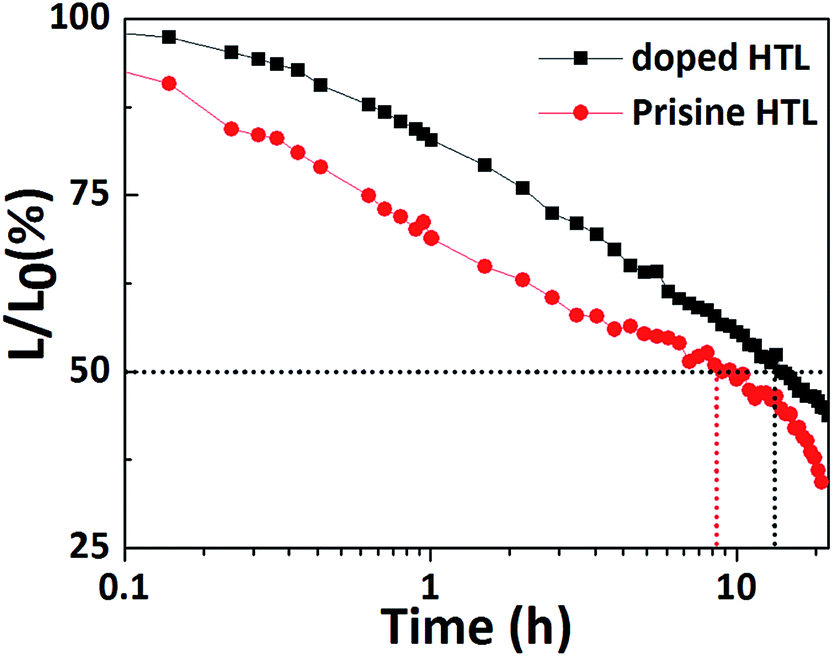 | ||
| Fig. 8 Stability data for QLEDs with different HTL. | ||
Conclusions
Highly efficient solution-processed QLED device with doped HTL composed of PVK and TAPC has been demonstrated. The doping ratio of PVK to TAPC was optimized based on the hole mobility, film quality and HOMO position of the HTL and confirmed at 3:1 at the end. The current efficiency, power efficiency and EQE increased to 26.2 cd A−1 and 19.2 lm W−1 and 6.2%, respectively. In addition, the stability of the device is enhanced due to the suppression of Auger recombination. This is attributed to balance of the carrier transport by modulating the hole transport utilizing doped HTL, which takes advantage of the superior energy level of PVK and high hole mobility of TAPC, while the film quality and energy barrier remain appropriate. The work presented here offers a strategy to obtain the highly efficient QLEDs via efficient and balanced carrier injection/transport, which can be achieved by engineering the HTL.
Conflicts of interest
There are no conflicts to declare.Acknowledgements
This work was supported partially by the National Key R&D Program of China (2016YFB0401600), National Natural Science Foundation Project (61674029, 61571124, and 61372030), Natural Science Foundation Project of Jiangsu Province (BK20151417), NSFC Research Fund for International Young Scientists (61550110243), the Jiangsu Province College Graduate Research Innovation Program under Grant (KYLX15_0100 and KYLX15_0101) and the Scientific Research Foundation of Graduate School of Southeast University YBJJ1714.References
- P. Reiss, J. Bleuse and A. Pron, Nano Lett., 2002, 2, 781–784 CrossRef CAS.
- J. J. Li, Y. A. Wang, W. Guo, J. C. Keay, T. D. Mishima, M. B. Johnson and X. Peng, J. Am. Chem. Soc., 2003, 125, 12567–12575 CrossRef CAS PubMed.
- Q. Sun, Y. A. Wang, L. S. Li, D. Wang, T. Zhu, J. Xu, C. Yang and Y. Li, Nat. Photonics, 2007, 1, 717–722 CrossRef CAS.
- P. O. Anikeeva, J. E. Halpert, M. G. Bawendi and V. Bulović, Nano Lett., 2009, 9, 2532–2536 CrossRef CAS PubMed.
- K.-S. Cho, E. K. Lee, W.-J. Joo, E. Jang, T.-H. Kim, S. J. Lee, S.-J. Kwon, J. Y. Han, B.-K. Kim, B. L. Choi and J. M. Kim, Nat. Photonics, 2009, 3, 341–345 CrossRef CAS.
- H. Shen, S. Wang, H. Wang, J. Niu, L. Qian, Y. Yang, A. Titov, J. Hyvonen, Y. Zheng and L. S. Li, ACS Appl. Mater. Interfaces, 2013, 5, 4260–4265 CAS.
- H. M. Kim, A. R. B. Yusoff, T. W. Kim, Y. G. Seol, H. P. Kim and J. Jang, J. Mater. Chem. C, 2014, 2, 2259–2265 RSC.
- X. Y. Yang, E. Mutlugun, C. Dang, K. Dev, Y. Gao, S. T. Tan, X. W. Sun and H. V. Demir, ACS Nano, 2014, 8, 8224–8231 CrossRef CAS PubMed.
- J. Y. Pan, J. Chen, Q. Q. Huang, Q. Khan, X. Liu, Z. Tao, W. Lei, F. Xua and Z. C. Zhang, RSC Adv., 2015, 5, 82192–82198 RSC.
- J. Pan, J. Chen, Q. Huang, Q. Khan, X. Liu, Z. Tao, Z. Zhang, W. Lei and A. Nathan, ACS Photonics, 2016, 3, 215–222 CrossRef CAS.
- J. Pan, J. Chen, D. Zhao, Q. Huang, Q. Khan, X. Liu, Z. Tao, Z. Zhang and W. Lei, Opt. Express, 2016, 24, A33–A43 CrossRef CAS PubMed.
- V. L. Colvin, M. C. Schlamp and A. P. Alivisatos, Nature, 1994, 370, 354–357 CrossRef CAS.
- V. I. Klimov, A. A. Mikhailovsky, S. Xu, A. Malko, J. A. Hollingsworth, C. A. Leatherdale, H. J. Eisler and M. G. Bawendi, Science, 2000, 290, 314 CrossRef CAS PubMed.
- E. Jang, S. Jun, H. Jang, J. Lim, B. Kim and Y. Kim, Adv. Mater., 2010, 22, 3076–3080 CrossRef CAS PubMed.
- O. E. Semonin, J. M. Luther, S. Choi, H.-Y. Chen, J. Gao, A. J. Nozik and M. C. Beard, Science, 2011, 334, 1530 CrossRef CAS PubMed.
- G. Konstantatos, I. Howard, A. Fischer, S. Hoogland, J. Clifford, E. Klem, L. Levina and E. H. Sargent, Nature, 2006, 442, 180–183 CrossRef CAS PubMed.
- X. Dai, Z. Zhang, Y. Jin, Y. Niu, H. Cao, X. Liang, L. Chen, J. Wang and X. Peng, Nature, 2014, 515, 96–99 CrossRef CAS PubMed.
- Y. Yang, Y. Zheng, W. Cao, A. Titov, J. Hyvonen, R. MandersJesse, J. Xue, P. H. Holloway and L. Qian, Nat. Photonics, 2015, 9, 259–266 CAS.
- P. O. Anikeeva, C. F. Madigan, J. E. Halpert, M. G. Bawendi and V. Bulovic, Phys. Rev. B: Condens. Matter Mater. Phys., 2008, 78, 085434 CrossRef.
- W. K. Bae, Y.-S. Park, J. Lim, D. Lee, L. A. Padilha, H. McDaniel, I. Robel, C. Lee, J. M. Pietryga and V. I. Klimov, Nat. Commun., 2013, 4, 3661 Search PubMed.
- V. Wood, M. J. Panzer, J. E. Halpert, J. M. Caruge, M. G. Bawendi and V. Bulović, ACS Nano, 2009, 3, 3581–3586 CrossRef CAS PubMed.
- J.-M. Caruge, J. E. Halpert, V. Bulović and M. G. Bawendi, Nano Lett., 2006, 6, 2991–2994 CrossRef CAS PubMed.
- T. Ding, X. Yang, L. Ke, Y. Liu, W.-Y. Tan, N. Wang, X.-H. Zhu and X. W. Sun, Org. Electron., 2016, 32, 89–93 CrossRef CAS.
- D.-H. Lee, Y.-P. Liu, K.-H. Lee, H. Chae and S. M. Cho, Org. Electron., 2010, 11, 427–433 CrossRef CAS.
- M. D. Ho, D. Kim, N. Kim, S. M. Cho and H. Chae, ACS Appl. Mater. Interfaces, 2013, 5, 12369–12374 CAS.
- X. Zhang, H. Dai, J. Zhao, S. Wang and X. Sun, Thin Solid Films, 2016, 603, 187–192 CrossRef CAS.
- Y. Tao, C. Yang and J. Qin, Chem. Soc. Rev., 2011, 40, 2943–2970 RSC.
- Q. Huang, J. Pan, Y. Zhang, J. Chen, Z. Tao, C. He, K. Zhou, Y. Tu and W. Lei, Opt. Express, 2016, 24, 25955–25963 CrossRef PubMed.
- N. A. Talik, K. H. Yeoh, C. Y. B. Ng, C. Y. Tan and B. K. Yap, J. Lumin., 2016, 169, 61–64 CrossRef CAS.
- P. Strohriegl and J. V. Grazulevicius, Adv. Mater., 2002, 14, 1439–1452 CrossRef CAS.
- Y. Shirota and H. Kageyama, Chem. Rev., 2007, 107, 953–1010 CrossRef CAS PubMed.
- P. Ravirajan, A. M. Peiro, M. K. Nazeeruddin, M. Graetzel, D. D. C. Bradley, J. R. Durrant and J. Nelson, J. Phys. Chem. B, 2006, 110, 7635–7639 CrossRef CAS PubMed.
- A. Castan, H. M. Kim and J. Jang, ACS Appl. Mater. Interfaces, 2014, 6, 2504–2511 Search PubMed.
- J.-H. Kim, C.-Y. Han, K.-H. Lee, K.-S. An, W. Song, J. Kim, M. S. Oh, Y. R. Do and H. Yang, Chem. Mater., 2015, 27, 197–204 CrossRef CAS.
- K. H. Lee, J. H. Lee, H. D. Kang, B. Park, Y. Kwon, H. Ko, C. Lee, J. Lee and H. Yang, ACS Nano, 2014, 8, 4893–4901 CrossRef CAS PubMed.
- L. Qian, Y. Zheng, J. G. Xue and P. H. Holloway, Nat. Photonics, 2011, 5, 543–548 CrossRef CAS.
- P. N. Murgatroyd, J. Phys. D: Appl. Phys., 1970, 3, 151 Search PubMed.
- Z. Khurelbaatar, K.-H. Shim, J. Cho, H. Hong, V. R. Reddy and C.-J. Choi, Mater. Trans., 2015, 56, 10–16 CrossRef CAS.
- P. Fu, X. Guo, Z. Wang, S. Yu, L. Zhou, W. Yu, J. Zhang and C. Li, RSC Adv., 2016, 6, 56845–56850 RSC.
- C. H. Cheung, W. J. Song and S. K. So, Org. Electron., 2010, 11, 89–94 CrossRef CAS.
| This journal is © The Royal Society of Chemistry 2017 |