DOI:
10.1039/C7RA07848J
(Paper)
RSC Adv., 2017,
7, 44136-44143
Thickness- and temperature-dependent structural and electromechanical properties of (100)-oriented Sc-doped (Na0.85K0.15)0.5Bi0.5TiO3 ferroelectric films
Received
17th July 2017
, Accepted 20th August 2017
First published on 13th September 2017
1. Introduction
The most widely used piezoelectric materials are Pb(Ti,Zr)O3 (PZT)-based three component systems. Because of the toxicity of lead oxide, it is desired to use lead-free piezoelectric materials in place of PZT for environmental protection. In recent years, bismuth sodium titanate (Na0.5Bi0.5)TiO3 (NBT) has been considered as one of the key lead-free piezoelectric materials and attracted considerable research attention.1–5 It is of a perovskite structure and has a relatively large remnant polarization, Pr = 38 μC cm−2, and high Curie temperature, TC = 320 °C. Recently, it has been reported that (Na0.5Bi0.5)TiO3 modified (K0.5Bi0.5)TiO3, 0.85(Na0.5Bi0.5)TiO3-0.15(K0.5Bi0.5)TiO3 (NKBT) bulk ceramics, showed improved dielectric and piezoelectric properties as a consequence of more ferroelectric variation in materials with compositions close to the morphotropic phase boundary (MPB).6–11 Because of substrate constraint effects and limited thicknesses, these factors will influences the phase structure and electrical properties, which make NBT films show inferior piezoelectric properties compared to bulk ceramic materials. Due to the effect of substrate constraints on the phase structure of textured thin films, a different thickness dependence of phase structure and properties will happen as for the film with composition changed to that close to the MPB. In addition, temperature dependence stability of properties is one of important characteristics in view of not only engineering but also basic physics point.
According to our research, an appropriated concentration Sc substitution in NKBT film could enhance piezoelectric properties and increase the Curie temperature.12 In this article, by introducing LaNiO3 (LNO) layer, (100)-oriented Sc-doped NKBT thin films, (Na0.85K0.15)0.5Bi0.5Ti0.75Sc0.25O3 (NKBT-Sc) were fabricated on Pt/Ti/SiO2/Si substrates by using aqueous sol–gel method. Two insertion modes of LNO were adopted. As for the first mode, a LNO layer was inserted at the interface between NKBT-Sc film and substrate; as for the second mode, LNO layers were inserted inside the film alternatively with NKBT-Sc layers, i.e., the composite film was prepared by depositing one LNO layer and four NKBT-Sc layers alternatively, forming a sandwich multilayer structured film. The schematic drawing of these two structured films are shown in Fig. 1. Based on these results, NKBT-Sc thickness- and temperature-dependent structural and electromechanical properties of the films were analyzed in detail. Based on these experiments, the mechanism of the variation was expounded systematically.
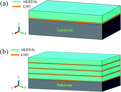 |
| | Fig. 1 The schematic drawing of the two structured films: (a) the first mode, (b) the second mode. | |
2. Experimental
2.1 Materials preparation
For preparation of NKBT-Sc film, bismuth nitrate [Bi(NO3)3·5H2O], tetrabutyl titanate [Ti(OC4H9)4], sodium acetate [NaCOOCH3], potassium acetate [KCOOCH3] and scandium acetate [Sc(COOCH3)3] were chosen as the raw materials with glacial acetic acid, isopropyl alcohol, and distilled water as the solvents. Firstly, a 1![[thin space (1/6-em)]](https://www.rsc.org/images/entities/char_2009.gif) :3:3 weight mixture of Ti(OC4H9)4, isopropyl alcohol, and acetylacetone was prepared. Then, glacial acid with 3:1 in volume ratio was poured into the mixture. Subsequently, a desired amount of Bi(NO)3 was dissolved in the solution, and distilled water with the same volume as the glacial acid was added. Here, 10% excess of bismuth nitrate was added to compensate for possible bismuth loss during the high temperature process. Finally, desired amounts of NaCOOCH3, KCOOCH3 and Sc(COOCH3)3 according to the (Na0.85K0.15)0.5Bi0.5Ti0.75Sc0.25O3 composition, were dissolved into the solution one by one. In order to prevent the appearance of cracks during aging and drying steps, an appropriate formamide was added into the above solution as a stabilizing agent during this process. During the whole preparation process, the precursor sol was carried out under constant stirring in air and at room temperature. The resultant solution, with a concentration of 0.26 M, was aged for ten days before deposition. For preparation of LNO layer, lanthanum nitrate [La(NO3)3] and nickel acetate [Ni(CH3COO)3] were dissolved into solvent with glacial acetic acid and ethylene glycol methyl ether [2-CH3OCH2CH2OH] under constant stirring. The resultant solution present clear green, with a concentration of 0.08 M, was stable and no crystallite forms for ten days before deposition.
:3:3 weight mixture of Ti(OC4H9)4, isopropyl alcohol, and acetylacetone was prepared. Then, glacial acid with 3:1 in volume ratio was poured into the mixture. Subsequently, a desired amount of Bi(NO)3 was dissolved in the solution, and distilled water with the same volume as the glacial acid was added. Here, 10% excess of bismuth nitrate was added to compensate for possible bismuth loss during the high temperature process. Finally, desired amounts of NaCOOCH3, KCOOCH3 and Sc(COOCH3)3 according to the (Na0.85K0.15)0.5Bi0.5Ti0.75Sc0.25O3 composition, were dissolved into the solution one by one. In order to prevent the appearance of cracks during aging and drying steps, an appropriate formamide was added into the above solution as a stabilizing agent during this process. During the whole preparation process, the precursor sol was carried out under constant stirring in air and at room temperature. The resultant solution, with a concentration of 0.26 M, was aged for ten days before deposition. For preparation of LNO layer, lanthanum nitrate [La(NO3)3] and nickel acetate [Ni(CH3COO)3] were dissolved into solvent with glacial acetic acid and ethylene glycol methyl ether [2-CH3OCH2CH2OH] under constant stirring. The resultant solution present clear green, with a concentration of 0.08 M, was stable and no crystallite forms for ten days before deposition.
A LNO layer of about 20 nm was spin-coated deposited on Pt/Ti/SiO2/Si substrate followed by sequentially drying at 100 °C for 10 min and pyrolyzing at 450 °C for 5 min. The as-deposited LNO layer was annealed at 600 °C and 700 °C for 2 min. The NKBT-Sc thin films were deposited onto LNO-coated substrates by spin coating at 4000 rpm for 30 s. After each coating, the films were dried at 100 °C for 10 min, and pyrolyzed at 450 °C for 5 min in ambient atmosphere. This processing was repeated different times to obtain a different thickness. As for the sandwich multilayer structured films with LNO layers inserted inside the NKBT-Sc film, after four NKBT-Sc layer have been deposited onto the LNO-coated substrate, then another LNO layer was deposited onto the as-prepared NKBT-Sc film, i.e. the films were prepared by depositing one LNO layer and four NKBT-Sc layers alternatively. All the films were finally annealed at 700 °C for 3 min by a rapid thermal processing in ambient atmosphere. For the electrical properties measurements, top electrodes of platinum, 0.2 mm in diameter, were sputtering deposited onto the surface of the films. Thereinafter, for sake of illustration, the NKBT-Sc/substrate film, the NKBT-Sc/LNO/substrate composite films and the composite films with LNO layers inside NKBT-Sc film, with various thicknesses of NKBT-Sc film, were denoted as N1, N2-x (x = ∼100, ∼200, ∼320, ∼460 and ∼620 nm) and N3-x respectively.
2.2 Characterization
Surface microstructures of these thin films were observed by scanning probe microscopy (SPM, SPI4000&SPA300HV, Seiko, Japan). The phase structures were characterized by X-ray diffraction (XRD, Rigaku, Japan) with Cu K-alpha radiation. Raman measurements were performed to detect the local structure changes within materials using an instrument of JY LabRam HR800 spectrometer (JOBIN YVON instrument Co., Longjumeau, France) in backscattering geometry. A ferroelectric test module (TF 2000 analyzer, axiACCT, Aachen, Germany) and a precision impedance analyzer (4294A, Agilent) were used to evaluate the ferroelectric and dielectric properties respectively. The piezoelectric properties of the films were measured by SPM under contact AFM mode, using an Rh-coated cantilever (Si-DF3-R, Seiko), which had a spring constant of 1.9 N m−1 and a free resonance frequency of 28 kHz.
3. Results and discussions
The crystal structure and preferential orientation were characterized by high-resolution XRD. Fig. 2 shows the XRD patterns of the N2 composite films with the NKBT-Sc thickness of about 460 nm, fabricated by annealing the LNO layer at 600 °C and 700 °C. Here, the N1 film was present for comparison. All of the diffraction peaks could be indexed according to the reference pattern of NBT powder (JCPDS 89-3109). It was found that all the films exhibited a pure perovskite structure with no trace of secondary phases detected. As for the single-layer N1 film, the (110) diffraction peak showed the highest intensity, while as for the N2 composite films, the (110) diffraction peak intensity weakened and the (100) diffraction peak intensity strengthened greatly, indicating an enhanced degree of the (100) orientation. Meanwhile, the averaged grain size D estimated according to Scherrer's equation (D = Kλ/FWHMcosθ, λ is the wavelength and FWHM is the full width at half maximum of the diffraction peaks) increased, indicating an enhanced degree of crystallinity. Moreover, it was observed that the N2 composite film with the LNO layer annealed at 700 °C exhibited a larger degree of (100) preferred orientation than that with LNO layer annealed at 600 °C. The formation of the (100) orientation was caused by the effect of LNO seeding layer on the surface of platinized silicon substrates.13
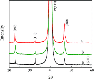 |
| | Fig. 2 XRD patterns for the (a) N1 film and the N2 composite films with the LNO layer annealed at (b) 600 °C, (c) 700 °C. | |
Fig. 3(a) shows the XRD patterns of the N2 composite films with various thicknesses of the NKBT-Sc film. Here, the LNO layer was annealed at 700 °C. A single perovskite phase structure and a preferred (100) orientation with no pyrochlore phase was detected in all the N2 composite films. In order to analyze phase structure of N2 composite films with various thicknesses, the step-scan XRD measurement on the (200) peaks was conducted and the results are shows in Fig. 3(b). A narrow and single (200) peak was obtained for the thinnest film of 100 nm thickness, and the location and shape suggested that the phase structure might be rhombohedral phase structure. Moreover, the location of the (200) peak shifted leftward and became broader generally with increasing thickness. As for the films with large thicknesses (∼460 and ∼620 nm), this phenomenon became pronounced and a broad sharp (200) peak was obtained, suggesting that more contributions from the tetragonal phase. As a result, a gradual change of phase structure from rhombohedral to tetragonal seem to occur with the increase of the NKBT-Sc film thickness.
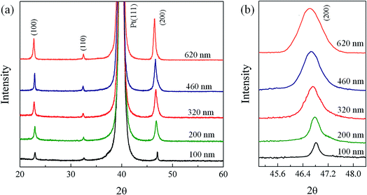 |
| | Fig. 3 (a) XRD pattern of the N2 composite films with various film thicknesses; (b) enlarged XRD pattern of the (200) peak. | |
These N2 composite films were further analyzed using Raman spectroscopy to give insight into the change in their phase structures, as shown in Fig. 4. According to the virtual ion model, the peaks at around 356 cm−1, 507 cm−1 and 611 cm−1, which was assigned to the Raman modes of tetragonal symmetry A1(2TO), E(3TO) and A1(3TO) respectively, were observed in films with thicknesses of about 620 nm.14 However, as the NKBT-Sc thickness decreased, the intensity of A1(2TO) peak got lower and became almost disappeared when thicknesses is about 320 nm. In the meantime, the E(3TO) and A1(3TO) peaks decreased and gradually evolved into a broad rhombohedral transverse mode (Rt)rhom at around 550 cm−1. Moreover, a peak at around 136 cm−1, which is attributed to characteristic Raman mode of rhombohedral phase, was observed in the composite film with NKBT-Sc thickness of about 320 nm. The intensity of this peak became weaker with increased thickness and disappeared as NKBT-Sc thickness above 460 nm, which indicated the formation of a higher degree of tetragonal phase. This observation is in good agreement with the XRD result. Thus, from the results of XRD and Raman analysis, as for the (100)-oriented N2 composite film with NKBT-Sc composition close to the MPB, a phase transition from a rhombohedral structure to a tetragonal occurred when the film thickness was varied from about 100 to 620 nm.
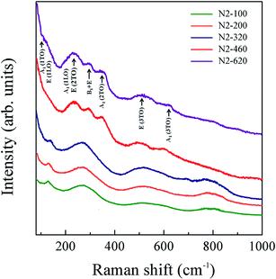 |
| | Fig. 4 Raman spectra of the N2 composite films with various film thicknesses. | |
For each film sample, the polarization–voltage curves with sequentially increasing voltages were measured at 100 Hz and the remnant polarization (Pr), extracted from the measure nested hysteresis loops. The ferroelectric hysteresis loops of the N2 composite films with different film thicknesses at 20 V are shown in Fig. 5 and the obtained thickness-dependent the Pr values is exhibited in the inset. The Pr value was found to increase gradually and reach a maximum of 23.7 μC cm−2 with film thickness of about 460 nm, and then decreased as the thickness was further increased. According to the XRD and Raman results, a phase structure transition occurred with the variation of film thickness, and during this process a two-phase coexistence existed in a proper film thickness region. In this region, polarization rotation from in-plane to out-of-plane will enhanced and hence result in an increase of Pr value. Furthermore, the better crystallinity in the highly (100) oriented could be also contributed to the increased Pr value. As the film thickness further increased, phase structure subsequently changed to a single phase, and consequently result in a lower Pr values. Thus, the remnant polarization exhibited a maximum with NKBT-Sc thickness at proper thickness.
 |
| | Fig. 5 Polarization–voltage hysteresis loops of the N2 composite films with various film thicknesses; the inset shows the thickness-dependent the remnant polarization. | |
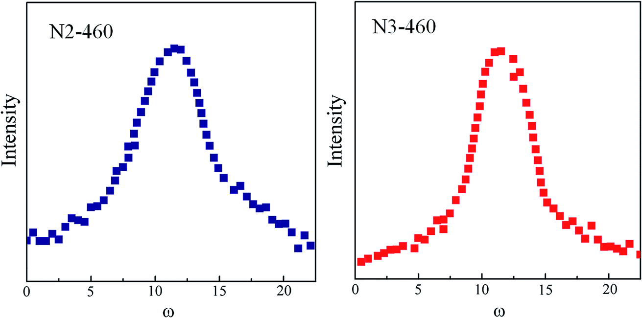
Fig. 6 shows XRD pattern of the N2-460 and N3-460 composite films. After the insertion of the LNO layers inside the NKBT-Sc film, the obtained N3 composite films exhibited a larger degree of (100) preferred orientation than that of N2 composite film. As for the N3 composite film, the LNO layers inside the NKBT-Sc film could play a role of nucleation and enhanced the density of grains along the (100) orientation, while as for the N2 composite film, the LNO layer inserted at the film–substrate interface had a weaker effect on the upper part of the NKBT-Sc films. This might be the main reason cause the higher (100) orientation of the N3 composite film than the N2 composite film. To observe the orientation distribution, ω-scan rocking curves of the (200) diffraction of the N2-460 and N3-460 composite films were measured, as showed in Fig. 7.15,16 During the measurement, the diffraction angle 2θhlk with respect to the diffracting plane (hkl) was fixed and the incidence angle ω of X-ray can be continuously changed from 0 to 2θhlk. Because XRD patterns of textured films are sensitive to incident X-ray beam angles, any small tilting of the film plane will cause substantial variation of the XRD peak position and intensity. According to Guo' report, the peak position and intensity of the same film sample could vary greatly in different measurements under the same instrument operating systems.17 Hence, to ensure precision of the data in peak position and intensity, this scans were measured by using a thin film diffractometer. Both the ω-scan XRD patterns were found to exhibit a symmetric Gauss distribution with the peak positions located approximately at the Bragg angle of corresponding diffraction planes. The FWHM of the N2 and N3 composite films were found to be 8.6 and 7.7, respectively, which meant that a higher distribution of grains along (001) orientation in the N3 composite film than the N2 composite film. Thus, these results indicated that the sandwich multilayer structured composite structure would further enhance the degree of the (001)-orientation.
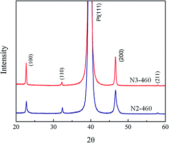 |
| | Fig. 6 XRD patterns of the N2-460 and N3-460 composite films. | |
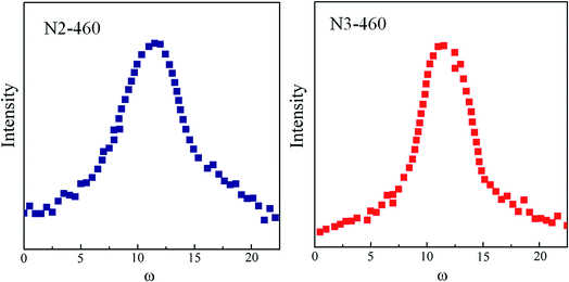 |
| | Fig. 7 XRD ω scan of the N2-460 and N3-460 composite films. | |
Fig. 8 shows the surface morphology of the LNO layer on the substrate and the N3-460 composite film. As shown in the figure, the LNO layer exhibited a dense microstructure without obvious defects such as holes and cracks observed. As for the N3 composite film, it exhibited a dense microstructure with a uniform grain size of about 40 nm.
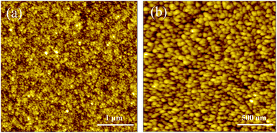 |
| | Fig. 8 Surface AFM images of (a) LNO layer deposited on substrate and (b) N3-460 composite film. | |
Since the composition of NKBT-Sc is close to the rhombohedral–tetragonal MPB, temperature may also induce phase structure evolution.18 Therefore, XRD was carried out at a temperature range of 20–300 °C on the N3-460 composite film to detect the structural change and the results are show in Fig. 9(a). A single perovskite phase structure with no detention of pyrochlore phase was exhibited in this temperature range. A high-resolution enlarged XRD at 2θ = 45–48° is used to characterize crystal structure with increasing testing temperature, shown in Fig. 9(b). A single sharp (200) peak is found in the temperature range of 20–180 °C, suggesting that the film was composed of an rhombohedral phase structure. As the temperature raise to about 240 °C, a trace of (002) shoulder of tetragonal structure appears. When the testing temperature reaches up to 300 °C, the (002) shoulder becomes pronounced, indicating more contributions from the tetragonal phase. Thus, a phase structure change seems to have occurred as the testing temperature gradually increases from 20 °C to 300 °C.
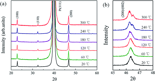 |
| | Fig. 9 (a) XRD pattern of the N3-460 composite film measured at a temperature range of 20 °C to 300 °C; (b) enlarged XRD pattern of the (200) peak. | |
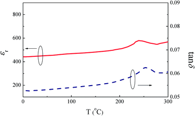
Temperature-dependent the dielectric properties εr and dissipation factors (tanδ) of the N3-460 composite film was given in Fig. 10. As measured at a temperature range of 20 °C to 300 °C, the dielectric constant gradually increased with increasing testing temperature. A shallow and broad dielectric hump was observed in the permittivity curve at about 260 °C. Moreover, this dielectric anomaly also appeared in the dielectric loss curve and some obvious at higher frequencies. With the increase of the testing temperature, tetragonal nanodomains generally grew and in the meantime the rhombohedral domains transform into nano-sized polar regions. Thus, this occurred hump hinted that the phase structure of the film was tend to transform from rhombohedral to tetragonal upon heating, which was consistent with the XRD result.
 |
| | Fig. 10 Temperature-dependent the dielectric constant and dielectric loss of the N3-460 composite film. | |
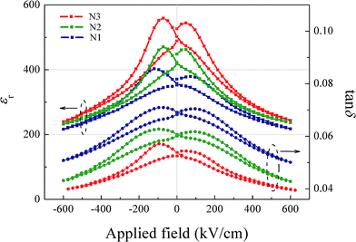
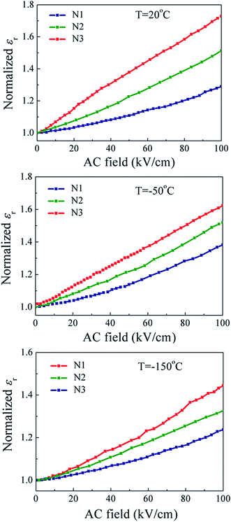
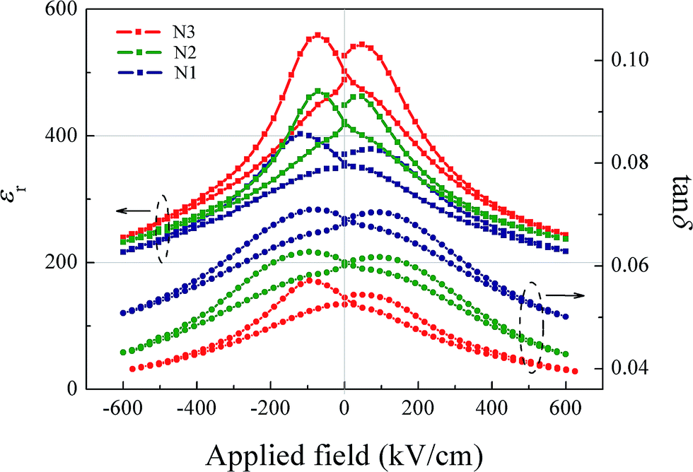
Fig. 11 shows the dielectric constant (εr) and dielectric loss (tanδ) vs. applied voltage curses of the film samples measured at 1 kHz. Here, the total thickness of NKBT-Sc layers is about 460 nm. The butterfly shape of the dielectric constant–applied voltage curve confirmed the ferroelectric characteristics of the film sample. The N3-460 composite film demonstrated the best dielectric properties in terms of the highest εr value of about 523 and the lowest tanδ of about 0.055. In addition, as the applied voltage increased, the difference of the εr value between these films gradually decreased and then became unpronounced at high applied voltage. Dielectric response includes intrinsic contribution and extrinsic contribution. The extrinsic contribution, which mainly come from domain wall motion and is more easier pinned, generally decreases as applied voltage increases. Thus, dielectric response at high DC applied field mainly comes from intrinsic contribution. This indicates that the difference of dielectric constant at zero DC applied field can be mainly attributed to extrinsic contribution, i.e. motion of domain walls. Besides, the domain wall pinned by defects at low AC field can contribute to the dielectric permittivity at higher AC field. Fig. 12 shows the dependence of the normalized dielectric constant on AC field of these films, measured at 20 °C, −50 °C and −150 °C. The dielectric constants increased linearly with increasing AC field, conforming to the Rayleigh relation.19 Rayleigh coefficient is calculated according to the slope of the curses and larger Rayleigh coefficient means there is a larger contribution of domain walls. The N3-460 composite film was found to exhibit the largest Rayleigh coefficient, indicating more domain walls responded and contributed to the dielectric constant at large AC field. As the testing temperature decreased from 20 °C to −150 °C, the dielectric constant of these films decreased generally and meanwhile the dielectric constant difference became smaller. Since domain wall movement is a thermally activated process, this decrease of the dielectric constant was mainly due to the lowered mobility of domain wall at low testing temperature.
 |
| | Fig. 11 Applied voltage-dependent the dielectric properties of the film samples. | |
 |
| | Fig. 12 AC field-dependent the dielectric constant of the film samples measured at different temperature. | |
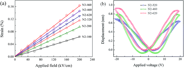
The piezoelectric response measurement was obtained by keeping the SPM tip fixed above the grain and applying a DC voltage while recording the signal. Fig. 13(a) shows the applied field-dependent the strain, which is obtained by measured displacement–voltage curve. The slope of the linear relationship between strain and applied voltage represents the effective piezoelectric coefficient  , and the calculated result were listed in Table 1. Typical displacement–applied voltage loops of the N2 composite films with NKBT-Sc thickness of about 320, 460 and 620 nm were shown in of Fig. 13(b). A similar trend was observed for the piezoelectric properties. As for the N2 composite films, the effective piezoelectric coefficients
  was found to increase from about 32 pm V−1 for the thinnest film to a peak value of about 73 pm V−1 when the film was about 460 nm thickness and then decreased with further increasing thickness. With the decrease of film thickness, the clamping of substrates and the effect of pinning centers at interface became pronounced. Since movement of domain walls might be a predominant contribution to the piezoelectric response, these effects will cause a lowered effective
  . In addition, the N3-460 composite film exhibited the best piezoelectric properties with the highest piezoelectric coefficients
  of about 82 pm V−1.
 |
| | Fig. 13 (a) Applied field-dependent the strain response; (b) displacement–applied voltage loops of the N2 composite films with various thicknesses. | |
Table 1 The effective piezoelectric coefficient  of the film samples
| Sample |
N2-100 |
N2-200 |
N2-320 |
N2-460 |
N2-620 |
N3-460 |
 |
32 |
48 |
60 |
73 |
65 |
82 |
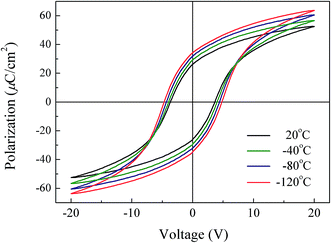
The polarization–applied voltage hysteresis loops of the N3-460 composite film were measured at a temperature range of 20 °C to −120 °C and the results were shown in Fig. 14. The Pr value of the N3-460 composite film at 20 °C was about 26.2 μC cm−2, larger than the N2-460 composite film. The LNO layers inside the NKBT-Sc film could play a role of nucleation and then further increased the crystallinity degree might the main reason caused this enlarged Pr. In addition, it was found that the remnant polarization Pr gradually increased with the decrease of the testing temperature from 20 °C to −120 °C, and in the meantime the coercive voltage (Vc) of the hysteresis loops, gradually moved to higher voltage. Change in remnant polarization may be affected by dipole switching, defects, and interface, etc. Potential wells are usually exists at the film–substrate interface. Charged defects, such as charged vacancies  and charged dipole
  ,20,21 are tend to trap at potential wells and form pinning centers. Thus, charged defects at the interface cause energy barrier and restricts dipole switching nearby. The dipole movement is thermally activated and it is more difficult for these pinned dipoles to switch. As the testing temperature decreases, dipole movement will suppressed by these pinning centers, and consequently a higher electric strength is needed to motivate ferroelectric dipoles to switch.22 Under this circumstance, more dipoles are frozen and their back-switching process will be restricted, leading to a higher Pr and larger Vc. When measuring at elevated temperature, the energy barrier for dipole switching under the electric field will reduce. Accordingly, the pinning-effect from the defects decreases and the N3 composite film exhibits a lower Pr.23,24 A similar phenomenon has also been found in some other perovskite structured ferroelectric film, such as PZT films.25
 |
| | Fig. 14 Polarization–voltage hysteresis loops of the N3-460 composite film measured at a temperature range of 20 °C to −120 °C. | |
4. Conclusion
By introducing LNO layer at film–substrate interface and inside the film, structure and electromechanical properties of the sol–gel-derived (100)-oriented Sc-doped (Na0.85K0.15)0.5Bi0.5TiO3 (NKBT-Sc) films deposited on Pt(111)/Ti/SiO2/Si(100) substrates were investigated. A phase structure transition from rhombohedral to tetragonal occurred when the NKBT-Sc thickness increased from ∼100 to ∼620 nm. The effective piezoelectric coefficients  was found to increase from about 32 pm V−1 for the thinnest film (∼100 nm) to a peak value of about 73 pm V−1 (∼460 nm) and then decreased with further increasing thickness, which showed a similar trend with the dielectric properties. The sandwich multilayer structured film by inserting LNO layers inside the NKBT-Sc film further enhanced the density of crystal grains along the (100) orientation and in favor of the crystallization process, leading to a better electromechanical properties of the films than the N2 composite film. The N3-460 composite film exhibited the piezoelectric coefficients
  of about 82 pm V−1, dielectric constant εr of about 523 and remnant polarization (Pr) of about 26.2 μC cm−2, with gradually increased with the decrease of the testing temperature from 20 °C to −120 °C, together with a low dielectric loss (tanδ) of about 0.055.
Conflicts of interest
There are no conflicts to declare.
Acknowledgements
The work was supported by the National Natural Science Foundation of China (51402020) and the Educational Commission of Hubei Province of China (Grant No. D20172803).
References
- Y. Chiang, G.-W. Farrey and A.-N. Soukhojak, Appl. Phys. Lett., 1998, 73, 3683–3685 CrossRef CAS.
- G.-O. Jones and P.-A. Thomas, Acta Crystallogr., Sect. B: Struct. Sci., 2000, 56, 426–430 Search PubMed.
- J. Kreisel, A.-M. Glazer, P. Bouvier and G. Lucazeau, Phys. Rev. B: Condens. Matter Mater. Phys., 2001, 63, 174106–174110 CrossRef.
- C. Feng, C.-H. Yang, F.-J. Geng, P.-P. Lv, Q. Yao and Q. Zhang, Ceram. Int., 2016, 42, 3531–3534 CrossRef CAS.
- Y.-L. Qin, S.-J. Zhang, Y.-Q. Wu, C.-J. Lua and J.-L. Zhang, J. Eur. Ceram. Soc., 2017, 37, 3493–3500 CrossRef CAS.
- A. Sasaki, T. Chiba, Y. Mamiya and E. Otsuki, Jpn. J. Appl. Phys., Part 1, 1999, 38, 5564–5567 CrossRef CAS.
- T. Yu, K.-W. Kwok and H.-L.-W. Chan, Mater. Lett., 2007, 61, 2117–2120 CrossRef CAS.
- Y.-Y. Wu, X.-H. Wang, C.-F. Zhong and L.-T. Li, Thin Solid Films, 2011, 519, 4798–4803 CrossRef CAS.
- S.-T. Zhang, B. Yang and W. Cao, Acta Mater., 2012, 60, 469–475 CrossRef CAS.
- Y.-Y. Wu, X.-H. Wang, C.-F. Zhong and L.-T. Li, J. Am. Ceram. Soc., 2011, 94, 1843–1849 CrossRef CAS.
- W.-H. Cui, X.-H. Wang and L.-T. Li, Ceram. Int., 2015, 41, S37–S40 CrossRef CAS.
- Y.-Y. Wu, X.-H. Wang and L.-T. Li, J. Am. Ceram. Soc., 2011, 94, 2518–2522 CrossRef CAS.
- Q.-G. Chi, J.-F. Dong, C.-H. Zhang, Y. Chen, X. Wang and Q. Q. Lei, J. Alloys Compd., 2017, 704, 336–342 CrossRef CAS.
- J. Wang, Z.-H. Zhou and J.-M. Xue, Acta Mater., 2006, 54, 1691–1698 CrossRef CAS.
- W.-D. Fei, C.-Q. Liu, M.-H. Ding, W.-L. Li and L.-D. Wang, Rev. Sci. Instrum., 2009, 80, 093903–093906 CrossRef CAS PubMed.
- W.-L. Li, Y. Zhao, W.-D. Fei, Q.-G. Chi and W.-T. Song, J. Sol-Gel Sci. Technol., 2010, 54, 335–339 CrossRef CAS.
- D. Guo, S. Ikeda, K. Saiki, H. Miyazoe and K. Terashima, J. Appl. Phys., 2006, 99, 094502–094507 CrossRef.
- N.-A. Pertsev, V.-G. Kukhar, H. Kohlstedt and R. Waser, Phys. Rev. B: Condens. Matter Mater. Phys., 2003, 67, 054107–054110 CrossRef.
- D.-V. Taylor and D. Damjanovic, J. Appl. Phys., 1997, 82, 1973–1975 CrossRef CAS.
- G. Arlt and H. Neumann, Ferroelectrics, 1988, 87, 109–120 CrossRef CAS.
- G.-E. Pike, W.-L. Warren, D. Dimos, B.-A. Tuttle, R. Ramesh, J. Lee, V.-G. Keramidas and J.-T. Evans Jr, Appl. Phys. Lett., 1995, 66, 484–486 CrossRef CAS.
- C.-F. Zhong, X.-H. Wang, J. Fang and L.-T. Li, J. Am. Ceram. Soc., 2010, 93, 3305–3311 CrossRef CAS.
- Y.-F. Wang, K. Cai, T.-M. Shao, Q. Zhao and D. Guo, J. Appl. Phys., 2015, 117, 164102–164107 CrossRef.
- K. Cai, F. Jiang, P. Y. Deng, J.-T. Ma and D. Guo, J. Am. Ceram. Soc., 2015, 98, 3165–3172 CrossRef CAS.
- F. Xu, S. Trolier-McKinstry, W. Ren, B. Xu, Z.-L. Xie and K.-J. Hemker, J. Appl. Phys., 2001, 89, 1336–1348 CrossRef CAS.
Footnote |
| † These authors contributed equally to this work. |
|
| This journal is © The Royal Society of Chemistry 2017 |
Click here to see how this site uses Cookies. View our privacy policy here. 
 Open Access Article
 This Open Access Article is licensed under a Creative Commons Attribution-Non Commercial 3.0 Unported Licence
 *a,
Yonghong Hu†b,
Xiaohui Wangc,
Caifu Zhongd and
Longtu Lic
*a,
Yonghong Hu†b,
Xiaohui Wangc,
Caifu Zhongd and
Longtu Lic
 initially increased from about 32 pm V−1 for the thinnest film (∼100 nm) to a peak value of about 73 pm V−1 (∼460 nm), but then decreased as the film thickness further increased. With the insertion of the LNO layers alternatively inside the NKBT-Sc film, the sandwich multilayer structure further enhanced the degree of the (001)-orientation and was beneficial for the crystallization process, leading to better electromechanical properties than the NKBT-Sc/LNO/substrate structure composite film. A high piezoelectric coefficient
 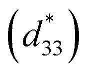 of about 82 pm V−1, dielectric constant εr of about 523 and remnant polarization (Pr) of about 26.2 μC cm−2, which gradually increased with the decrease of the testing temperature from 20 °C to −120 °C, together with a with a low dielectric loss (tan


 , and the calculated result were listed in Table 1. Typical displacement–applied voltage loops of the N2 composite films with NKBT-Sc thickness of about 320, 460 and 620 nm were shown in of Fig. 13(b). A similar trend was observed for the piezoelectric properties. As for the N2 composite films, the effective piezoelectric coefficients
  was found to increase from about 32 pm V−1 for the thinnest film to a peak value of about 73 pm V−1 when the film was about 460 nm thickness and then decreased with further increasing thickness. With the decrease of film thickness, the clamping of substrates and the effect of pinning centers at interface became pronounced. Since movement of domain walls might be a predominant contribution to the piezoelectric response, these effects will cause a lowered effective
  . In addition, the N3-460 composite film exhibited the best piezoelectric properties with the highest piezoelectric coefficients
  of about 82 pm V−1.
 of the film samples

 and charged dipole
  ,20,21 are tend to trap at potential wells and form pinning centers. Thus, charged defects at the interface cause energy barrier and restricts dipole switching nearby. The dipole movement is thermally activated and it is more difficult for these pinned dipoles to switch. As the testing temperature decreases, dipole movement will suppressed by these pinning centers, and consequently a higher electric strength is needed to motivate ferroelectric dipoles to switch.22 Under this circumstance, more dipoles are frozen and their back-switching process will be restricted, leading to a higher Pr and larger Vc. When measuring at elevated temperature, the energy barrier for dipole switching under the electric field will reduce. Accordingly, the pinning-effect from the defects decreases and the N3 composite film exhibits a lower Pr.23,24 A similar phenomenon has also been found in some other perovskite structured ferroelectric film, such as PZT films.25
 was found to increase from about 32 pm V−1 for the thinnest film (∼100 nm) to a peak value of about 73 pm V−1 (∼460 nm) and then decreased with further increasing thickness, which showed a similar trend with the dielectric properties. The sandwich multilayer structured film by inserting LNO layers inside the NKBT-Sc film further enhanced the density of crystal grains along the (100) orientation and in favor of the crystallization process, leading to a better electromechanical properties of the films than the N2 composite film. The N3-460 composite film exhibited the piezoelectric coefficients
  of about 82 pm V−1, dielectric constant εr of about 523 and remnant polarization (Pr) of about 26.2 μC cm−2, with gradually increased with the decrease of the testing temperature from 20 °C to −120 °C, together with a low dielectric loss (tan