
 Open Access Article
 This Open Access Article is licensed under a Creative Commons Attribution-Non Commercial 3.0 Unported Licence
Selective and confined growth of transition metal dichalcogenides on transferred graphene†
Fei Lu a,
Arka Karmakara,
Simran Shahia and
Erik Einarsson*ab
a,
Arka Karmakara,
Simran Shahia and
Erik Einarsson*ab
aDepartment of Electrical Engineering, University at Buffalo, Buffalo, NY, USA. E-mail: erikeina@buffalo.edu
bDepartment of Materials Design and Innovation, University at Buffalo, Buffalo, NY, USA
First published on 27th July 2017
Abstract
We demonstrate confinement of CVD grown MoS2 to a patterned graphene area, forming a vertically stacked 2D heterostructure. The CVD-grown graphene had been transferred onto a Si wafer and patterned using photolithography. Raman mapping and spectral analysis reveal few-layer MoS2 grew selectively on graphene regions, and not on the surrounding SiO2 substrate surface. We also report CVD growth of WS2 directly on transferred graphene. Unlike MoS2, no few-layer regions were found; the WS2 was found to be either monolayer or at least five layers (bulk). The WS2 coverage was only partial, but selectivity to graphene is apparent. These findings have the potential to significantly advance fabrication of vertical 2D heterostructures and related devices, and suggest the selective growth on graphene may be applicable to TMDCs in general.
1 Introduction
As we continue to improve our understanding of two-dimensional (2D) materials, the focus of interest shifts increasingly toward 2D heterostructures. The atomically sharp interfaces in these so-called van der Waals solids give rise to unique properties that depend on the characteristics of their constituent layers.1 Graphene and transition metal dichalcogenides (TMDCs) are the most thoroughly investigated 2D materials to date, and heterostructures based on these materials have yielded numerous potential applications including photodetectors,2,3 photoresponsive memory devices,4 field-effect transistors,5,6 and quantum-well light-emitting diodes.7 Many of these devices are based on vertically stacked 2D heterostructures, which are typically fabricated in one of three ways. One method is mechanical exfoliation, followed by manually picking and placing the exfoliated material at the desired location.4,6,8 A second method is TMDC synthesis atop epitaxial graphene grown on a SiC substrate,9–13 and a third is TMDC synthesis on graphene that has been transferred onto a silicon or quartz substrate.2,3,5 One challenge common to all these methods is how to define the locations of these 2D heterostructures prior to growth. This hurdle must be overcome before fabrication techniques can be scaled beyond single elements.Here we report CVD growth of molybdenum disulfide (MoS2) directly atop, and laterally confined by, an underlying graphene pattern. We also report CVD synthesis of tungsten disulfide (WS2) directly on graphene. While the WS2 coverage was not complete, growth was selective to graphene and did not occur on the SiO2 substrate surface. These results are an important step toward the ability to pre-define the growth location of 2D heterostructures by patterned graphene templates.
2 Experimental
To produce vertically stacked TMDC–graphene heterostructures, we first synthesized graphene at 1000 °C on copper foil using low-pressure chemical vapor deposition (CVD). We then transferred the graphene onto a silicon substrate with a 285 nm oxide layer (SiO2/Si). This was done using an unpublished variation on a widely used wet process,14,15 in which we use a copolymer layer in addition to a layer of poly(methyl methacrylate) (PMMA). We then used the graphene-on-SiO2/Si as a substrate for TMDC growth (MoS2 and WS2). In the case of MoS2 growth, we patterned the transferred graphene prior to CVD using standard photolithography techniques.We grew MoS2 by CVD in a tube furnace at 700 °C and atmospheric pressure. We prepared the molybdenum source by dispersing MoO3 powder in ethanol, and then dropping the dispersion onto a 5 × 5 mm piece of silicon wafer.16 After the ethanol evaporated, approximately 10 mg of MoO3 remained. We then placed the patterned graphene-on-SiO2/Si centered directly above the MoO3 source at a distance of approximately 7 mm, with the patterned graphene side facing toward the MoO3. The sulfur source was placed 30 cm upstream from the MoO3 source (10 cm outside the furnace), and heated separately using a heating belt. Prior to CVD, we purged air from the system by evacuating the quartz tube (26 mm ID) and refilling to atmospheric pressure using pure Ar gas. We continued to supply Ar at a flow rate of 150 sccm throughout the entire CVD process. We increased the furnace temperature by 20 °C per minute until reaching 700 °C, at which point the temperature was held constant for the duration of growth (10 min). The sulfur source was kept at 200 °C throughout. An overview of the process is illustrated in Fig. 1.
 | ||
| Fig. 1 Illustration of processing steps (clockwise from top left) resulting in localized CVD growth of MoS2 on patterned graphene. | ||
The process for WS2 growth was similar to that for MoS2, except that growth occurred at 900 °C instead of 700 °C. One minor difference is a longer growth time for WS2 (15 min instead of 10 min). The tungsten source was also prepared as is common for CVD growth of WS2, but this is different to the Mo source preparation. We simply placed 100 mg of WO3 powder in a quartz boat and positioned it below the target substrate as described above. The placement of the sulfur source was identical in both cases, but we note that these growth procedures have not been fully optimized.
After TMDC growth, we characterized the results using optical microscopy and Raman spectroscopy. We used a Renishaw inVia Reflex micro-Raman spectrometer to collect Raman spectra and perform mapping. Excitation laser wavelengths were 514 nm for MoS2 and 488 nm for WS2 in order to avoid strong resonances at 514 nm.17
3 Results and discussion
3.1 MoS2 growth localized to patterned graphene
The top row of Fig. 2(a)–(c) shows an optical micrograph of as-grown MoS2–graphene heterostructures and two superimposed Raman intensity maps. The Raman map in Fig. 2(b) shows the graphene 2D peak intensity, confirming graphene in the patterned rectangles. The other Raman map in Fig. 2(c) shows the integrated intensity of the two characteristic MoS2 peaks found between 370 cm−1 and 420 cm−1. Both Raman maps correspond to the same area, confirming MoS2 growth was directly atop, and confined by, patterned graphene. | ||
| Fig. 2 (a) Optical micrograph of patterned graphene on SiO2/Si. Scale bar corresponds to 20 μm. (b and c) Superimposed Raman maps showing MoS2 growth corresponds exactly to graphene pattern regions. (b) Intensity of graphene 2D peak at 2711 cm−1 and (c) integrated intensity of MoS2 E12g and A1g peaks (from 370 to 420 cm−1). (d) Raman spectra of (i) graphene, (ii) MoS2 on graphene, and (iii–v) annealed versions of both. All spectra are normalized to the first-order silicon peak (hidden), and λex = 514 nm. (e) Decomposition of Raman spectrum after CVD of MoS2 on graphene ((ii) in (d)). | ||
In the upper panel of Fig. 2d, we show Raman spectra before and after MoS2 growth on graphene. These are labeled (i) and (ii), respectively. In addition to the graphene G and 2D peaks,18 additional peaks appear after MoS2 growth. Based on the decomposition and fitting shown in Fig. 2e, we attribute the small, emergent Raman peaks located at 1259 cm−1 and 1456 cm−1 to C–H stretching and bending modes.19 Although these peaks only appear when sulfur is supplied, the positions and relative intensities more closely match peaks associated with C–H than C–S bonds.20 The origin of hydrogen, however, is not clear. We attribute the larger peaks at 1376 cm−1, 1559 cm−1, and 2887 cm−1 to the D, G, and 2D peaks of amorphous carbon (Da-C, Ga-C, 2Da-C).21
In the lower panel of Fig. 2d we show Raman spectra from graphene-on-SiO2/Si annealed at the MoS2 growth temperature (700 °C). When annealed under pure Ar (Fig. 2d(iii)), no peaks associated with a-C appear. When annealed in the presence of sulfur but in the absence of MoO3 (Fig. 2d(iv)), a-C peaks are clearly visible, and the spectrum is very similar to that of MoS2 grown on graphene (Fig. 2d(ii)). These results indicate that a-C formation is not simply due to elevated temperature, but the presence of sulfur at elevated temperature.20 In spite of this, the amount of a-C can be reduced by annealing in a sulfur environment at even higher temperature. This is shown in Fig. 2d(v), which corresponds to MoS2 on graphene annealed at 900 °C for 20 min in the presence of sulfur. We note that the a-C Raman modes have considerably lower relative intensity, whereas the other peaks remain largely unchanged.
All spectra in Fig. 2d exhibit an upshift of the graphene G and 2D peaks, as well as broadening of the 2D peak relative to the as-transferred graphene. These changes suggest hole doping of the graphene occurs during thermal treatment22,23 and subsequent exposure to the atmosphere.24
Based on the positions of the MoS2 E12g and A1g Raman modes,25,26 we find the MoS2 thickness ranges from two layers to five or more layers (bulk), with the majority being three or four layers of MoS2. We found the layer number to be very sensitive to the local MoO3 concentration. Near the center of the substrate, where the MoO3 concentration is highest (i.e., directly above the MoO3 source), we find MoS2 can nucleate and grow directly on the silicon wafer, but is predominantly bulk. Closer to the substrate edge, where the MoO3 concentration is lower, few-layer MoS2 selectively grows only on graphene. Our hypothesis for the selective growth on graphene is as follows. Since sulfur is introduced to the system from the beginning of the CVD process, it can satisfy dangling bonds present in graphene. When the growth temperature is reached and Mo is present, the attached sulfur atoms act as nucleation sites, leading to selective growth of MoS2 on graphene. This mechanism should also apply to other TMDCs under appropriate conditions, and the following results for WS2 suggest that to be the case.
3.2 WS2 grown directly on graphene
Fig. 3a shows an optical image of WS2 grown on graphene by CVD. We note that patterned graphene was not used here. Instead, we reduced the CVD time in order to avoid forming continuous graphene, and then grew WS2 atop that. Raman intensity maps of the graphene 2D and WS2 E12g peaks are shown in Fig. 3b and c. The mapped area corresponds to the dotted outline in Fig. 3a. Comparing the Raman maps with the optical micrograph, we see that the majority of the surface is covered by graphene, but only some of the graphene is covered by WS2. Darker regions in (a) are WS2 on top of graphene, whereas bright spots correspond to bulk WS2 (five or more layers). A few graphene voids are visible as slightly lighter patches. WS2 appears to grow right up to the edge of several of these voids, but does not extend out onto the SiO2 surface. This indicates that WS2 grows selectively on graphene, as was the case for MoS2.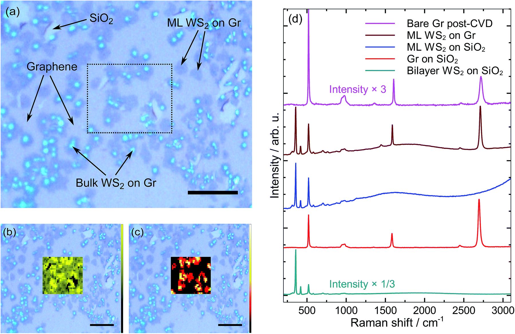 | ||
| Fig. 3 (a) Optical micrograph of WS2 grown on graphene. Dotted line denotes mapped area shown in (b and c). All scale bars are 20 μm, and λex = 488 nm. (b) Intensity map of graphene 2D peak at 2727 cm−1. (c) Intensity map of E12g peak of monolayer WS2 at 354.9 cm−1. (d) Raman spectra of graphene and WS2 with different interfacial conditions. The topmost two spectra are from the map at left, whereas the lower three spectra are from different processes and shown for comparison. All spectra are normalized to the first-order silicon peak. | ||
In Fig. 3d we plot various Raman spectra for comparison. The top two spectra are from the Raman maps shown, whereas the bottom three spectra are from different processes but shown for comparison and clarification. Our analysis reveals several similarities with MoS2 grown on graphene. For example, we find C–H peaks in the Raman spectra for both cases. Despite the presence of sulfur during WS2 growth at 900 °C, no obvious a-C Raman peaks are found. This is consistent with our finding that annealing MoS2 at this temperature in a sulfur environment reduced the amount of a-C. Lowering the WS2 growth temperature from 900 °C to 850 °C increased coverage of WS2 on graphene, but the quality of graphene suffered (i.e., strong C–H and a-C peaks appeared).
Based on the E12g and A1g peak separation,17 one significant difference between WS2 on graphene and MoS2 on graphene is that we find no few-layer regions of WS2. The WS2 grown on graphene is either monolayer (ML) or bulk (5+ layers). Importantly, we noticed small shifts in the E12g and A1g peak positions for ML WS2 on graphene compared to ML WS2 on SiO2/Si. The E12g peak position shifts down slightly from 355.6 cm−1 to 355.1 cm−1, whereas the A1g peak shifts up slightly from 417.2 cm−1 to 417.6 cm−1. This is only slightly larger than the uncertainty of 0.3 cm−1, but the shift is consistent for more than 10 independent measurements. We find the E12g and A1g peak separation for monolayer WS2 on graphene to be 62.5 cm−1. This is slightly larger than the 61.6 cm−1 for WS2 on SiO2, yet still less than the 63.4 cm−1 that corresponds to bilayer WS2 on SiO2.17
By comparing the WS2 E12g and A1g peak intensities to the Si substrate peak at 520 cm−1, we can confirm the darker regions seen in Fig. 3a are indeed monolayer rather than bilayer WS2 on graphene. The presence of a fluorescence tail (onset visible near 3000 cm−1) is further evidence that the spectrum labeled “ML WS2 on SiO2” is indeed monolayer. The absence of this tail for monolayer WS2 on graphene is due to ultrafast charge transfer to graphene,27 indicating a clean and sharp interface in the heterostructure. Moreover, the strong Raman signal suggests graphene quality remains high despite the high-temperature growth environment.
4 Conclusion
In conclusion, we report CVD growth of few-layer MoS2 directly atop patterned graphene in which the MoS2 is confined to the graphene region. The MoS2 covered the entire graphene pattern, demonstrating the ability to define the shape and location of vertically stacked 2D heterostructures prior to CVD. We also report WS2 selectively grown on transferred graphene. Unlike MoS2, coverage of WS2 was incomplete, and was found to be either bulk or monolayer. Obtaining complete coverage of WS2 should be a matter of finding appropriate growth conditions and is left for future study. For both MoS2 and WS2, we hypothesize that sulfur atoms that satisfy dangling bonds on the graphene act as nucleation sites, confining the growth location. Similar findings using two different TMDCs, despite considerably different growth conditions, suggests this graphene-templated selective growth may apply to TMDCs in general. We expect these results will facilitate batch fabrication of 2D heterostructure systems and devices.Acknowledgements
This work was supported by Award FA9550-16-1-0188 from the Air Force Office of Scientific Research, and by the Innovative Micro-Programs Accelerating Collaboration in Themes (IMPACT) program funded by the Office of Vice President of Research and Economic Development at the University at Buffalo.References
- A. C. Ferrari, F. Bonaccorso, V. Fal'ko, K. S. Novoselov, S. Roche, P. Bøggild, S. Borini, F. H. L. Koppens, V. Palermo, N. Pugno, J. A. Garrido, R. Sordan, A. Bianco, L. Ballerini, M. Prato, E. Lidorikis, J. Kivioja, C. Marinelli, T. Ryhänen, A. Morpurgo, J. N. Coleman, V. Nicolosi, L. Colombo, A. Fert, M. Garcia-Hernandez, A. Bachtold, G. F. Schneider, F. Guinea, C. Dekker, M. Barbone, Z. Sun, C. Galiotis, A. N. Grigorenko, G. Konstantatos, A. Kis, M. Katsnelson, L. Vandersypen, A. Loiseau, V. Morandi, D. Neumaier, E. Treossi, V. Pellegrini, M. Polini, A. Tredicucci, G. M. Williams, B. H. Hong, J.-H. Ahn, J. M. Kim, H. Zirath, B. J. van Wees, H. van der Zant, L. Occhipinti, A. Di Matteo, I. A. Kinloch, T. Seyller, E. Quesnel, X. Feng, K. Teo, N. Rupesinghe, P. Hakonen, S. R. T. Neil, Q. Tannock, T. Löfwander and J. Kinaret, Nanoscale, 2015, 7, 4598–4810 RSC.
- C. Chen, Z. Feng, Y. Feng, Y. Yue, C. Qin, D. Zhang and W. Feng, ACS Appl. Mater. Interfaces, 2016, 8, 19004–19011 CAS.
- W. Zhang, C.-P. Chuu, J.-K. Huang, C.-H. Chen, M.-L. Tsai, Y.-H. Chang, C.-T. Liang, Y.-Z. Chen, Y.-L. Chueh, J.-H. He, M.-Y. Chou and L.-J. Li, Sci. Rep., 2014, 4, 3826 CrossRef PubMed.
- K. Roy, M. Padmanabhan, S. Goswami, T. P. Sai, G. Ramalingam, S. Raghavan and A. Ghosh, Nat. Nanotechnol., 2013, 8, 826–830 CrossRef CAS PubMed.
- M. Zhao, Y. Ye, Y. Han, Y. Xia, H. Zhu, S. Wang, Y. Wang, D. A. Muller and X. Zhang, Nat. Nanotechnol., 2016, 11, 954–959 CrossRef CAS PubMed.
- T. Georgiou, R. Jalil, B. D. Belle, L. Britnell, R. V. Gorbachev, S. V. Morozov, Y.-J. Kim, A. Gholinia, S. J. Haigh, O. Makarovsky, L. Eaves, L. A. Ponomarenko, A. K. Geim, K. S. Novoselov and A. Mishchenko, Nat. Nanotechnol., 2013, 8, 100–103 CrossRef CAS PubMed.
- F. Withers, O. Del Pozo-Zamudio, A. Mishchenko, A. P. Rooney, A. Gholinia, K. Watanabe, T. Taniguchi, S. J. Haigh, A. K. Geim, A. I. Tartakovskii and K. S. Novoselov, Nat. Mater., 2015, 14, 301–306 CrossRef CAS PubMed.
- L. Britnell, R. M. Ribeiro, A. Eckmann, R. Jalil, B. D. Belle, A. Mishchenko, Y.-J. Kim, R. V. Gorbachev, T. Georgiou, S. V. Morozov, A. N. Grigorenko, A. K. Geim, C. Casiraghi, A. H. Castro Neto and K. S. Novoselov, Science, 2013, 340, 1311–1314 CrossRef CAS PubMed.
- Y. Shi, W. Zhou, A.-Y. Lu, W. Fang, Y.-H. Lee, A. L. Hsu, S. M. Kim, K. K. Kim, H. Y. Yang, L.-J. Li, J.-C. Idrobo and J. Kong, Nano Lett., 2012, 12, 2784–2791 CrossRef CAS PubMed.
- C. E. Giusca, I. Rungger, V. Panchal, C. Melios, Z. Lin, Y.-C. Lin, E. Kahn, A. L. Elías, J. A. Robinson, M. Terrones and O. Kazakova, ACS Nano, 2016, 10, 7840–7846 CrossRef CAS PubMed.
- A. Rossi, H. Büch, C. D. Rienzo, V. Miseikis, D. Convertino, A. Al-Temimy, V. Voliani, M. Gemmi, V. Piazza and C. Coletti, 2D Materials, 2016, 3, 031013 CrossRef.
- Y.-C. Lin, C.-Y. S. Chang, R. K. Ghosh, J. Li, H. Zhu, R. Addou, B. Diaconescu, T. Ohta, X. Peng, N. Lu, M. J. Kim, J. T. Robinson, R. M. Wallace, T. S. Mayer, S. Datta, L.-J. Li and J. A. Robinson, Nano Lett., 2014, 14, 6936–6941 CrossRef CAS PubMed.
- D. Pierucci, H. Henck, C. H. Naylor, H. Sediri, E. Lhuillier, A. Balan, J. E. Rault, Y. J. Dappe, F. Bertran, P. L. Fèvre, A. T. C. Johnson and A. Ouerghi, Sci. Rep., 2016, 6, 26656 CrossRef CAS PubMed.
- X. Li, Y. Zhu, W. Cai, M. Borysiak, B. Han, D. Chen, R. D. Piner, L. Colombo and R. S. Ruoff, Nano Lett., 2009, 9, 4359–4363 CrossRef CAS PubMed.
- G. B. Barin, Y. Song, I. F. Gimenez, A. G. Souza Filho, L. S. Barreto and J. Kong, Carbon, 2015, 84, 82–90 CrossRef.
- Z. Lin, Y. Zhao, C. Zhou, R. Zhong, X. Wang, Y. H. Tsang and Y. Chai, Sci. Rep., 2015, 5, 18596 CrossRef CAS PubMed.
- A. Berkdemir, H. R. Gutiérrez, A. R. Botello-Méndez, N. Perea-López, A. L. Elías, C.-I. Chia, B. Wang, V. H. Crespi, F. López-Urías, J.-C. Charlier, H. Terrones and M. Terrones, Sci. Rep., 2013, 3, 1–8 Search PubMed.
- A. C. Ferrari, J. C. Meyer, V. Scardaci, C. Casiraghi, M. Lazzeri, F. Mauri, S. Piscanec, D. Jiang, K. S. Novoselov, S. Roth and A. K. Geim, Phys. Rev. Lett., 2006, 97, 187401 CrossRef CAS PubMed.
- H. Wu, J. V. Volponi, A. E. Oliver, A. N. Parikh, B. A. Simmons and S. Singh, Proc. Natl. Acad. Sci. U. S. A., 2011, 108, 3809–3814 CrossRef CAS PubMed.
- L. Zhang, L. Ji, P.-A. Glans, Y. Zhang, J. Zhu and J. Guo, Phys. Chem. Chem. Phys., 2012, 14, 13670–13675 RSC.
- J. Hong, M. K. Park, E. J. Lee, D. Lee, D. S. Hwang and S. Ryu, Sci. Rep., 2013, 3, 2700 CrossRef PubMed.
- S. Ryu, L. Liu, S. Berciaud, Y.-J. Yu, H. Liu, P. Kim, G. W. Flynn and L. E. Brus, Nano Lett., 2010, 10, 4944–4951 CrossRef CAS PubMed.
- J. E. Lee, G. Ahn, J. Shim, Y. S. Lee and S. Ryu, Nat. Commun., 2012, 3, 1024 CrossRef PubMed.
- L. Liu, S. Ryu, M. R. Tomasik, E. Stolyarova, N. Jung, M. S. Hybertsen, M. L. Steigerwald, L. E. Brus and G. W. Flynn, Nano Lett., 2008, 8, 1965–1970 CrossRef CAS PubMed.
- C. Lee, H. Yan, L. E. Brus, T. F. Heinz, J. Hone and S. Ryu, ACS Nano, 2010, 4, 2695–2700 CrossRef CAS PubMed.
- H. Li, Q. Zhang, C. C. R. Yap, B. K. Tay, T. H. T. Edwin, A. Olivier and D. Baillargeat, Adv. Funct. Mater., 2012, 22, 1385–1390 CrossRef CAS.
- J. He, N. Kumar, M. Z. Bellus, H.-Y. Chiu, D. He, Y. Wang and H. Zhao, Nat. Commun., 2014, 5, 5622 CrossRef CAS PubMed.
Footnote |
| † Electronic supplementary information (ESI) available: Optical micrograph of MoS2 on graphene, details regarding the curve fitting analysis of Raman spectra, and additional Raman spectra of MoS2 on graphene, WS2 on graphene, and graphene under various conditions are included. See DOI: 10.1039/c7ra07772f |
| This journal is © The Royal Society of Chemistry 2017 |