
 Open Access Article
 This Open Access Article is licensed under a
 Creative Commons Attribution 3.0 Unported Licence
BiFeO3 nanorings synthesized via AAO template-assisted pulsed laser deposition and ion beam etching
Guo Tiana,
Deyang Chen *a,
Junxiang Yaoa,
Qiuyuan Luoa,
Zhen Fana,
Min Zenga,
Zhang Zhanga,
Jiyan Daib,
Xingsen Gao*a and
Jun-Ming Liuc
*a,
Junxiang Yaoa,
Qiuyuan Luoa,
Zhen Fana,
Min Zenga,
Zhang Zhanga,
Jiyan Daib,
Xingsen Gao*a and
Jun-Ming Liuc
aInstitute for Advanced Materials (IAM), Guangdong Provincial Key Laboratory of Quantum Engineering and Quantum Materials, South China Normal University, Guangzhou 510006, China. E-mail: dychen1987@gmail.com; xingsengao@scnu.edu.cn
bDepartment of Applied Physics, Hong Kong Polytechnic University, Hong Kong, China
cLaboratory of Solid State Microstructures, Innovation Center of Advanced Microstructures, Nanjing University, 210093, China
First published on 23rd August 2017
Abstract
We propose a novel and facile method to fabricate epitaxial ferroelectric BiFeO3 (BFO) nanorings using anodized alumina (AAO) template-assisted PLD and ion-beam etching. The morphology and dimensions of these nanorings are revealed by atomic force microscopy (AFM) and confirmed by transmission electron microscopy (TEM). The typical dimensions of the BFO nanorings are 12 nm inner diameter with 30 nm wall thickness and heights of around 10 nm. The X-ray diffraction (XRD), reciprocal space mapping (RSM) and TEM data demonstrate the epitaxial structure of these nanorings. Moreover, the ferroelectric properties are investigated by piezoresponse force microscopy (PFM), showing the polarization reversal behaviors of the isolated BFO nanorings, which have great potential applications for high-density non-volatile memory devices. In addition, this novel method could also be extended to other material systems (such as BaTiO3, ZnO and Au). Furthermore, the fabrication of high quality nanoring structures may open a pathway to explore related emerging physical phenomena (e.g., ferroelectric vortices).
Introduction
Currently ferroelectric nanorings are attracting a great deal of interest mainly for two reasons. First, ferroelectric nanorings have potential applications in next generation, high-density, and non-volatile memory devices.1–3 Second, a new state of matter called ferroelectric vortices (toroidal ordering of dipoles) has been theoretically predicted in ferroelectric nanorings (due to the release of the strain energy in the core), which would provide a new platform for the study of fascinating physical phenomena and as a novel ferroelectric memory in data storage.2,4–8 Very recently, the flux-closure domains and polar vortices were observed in PbTiO3/SrTiO3 multilayers9 and their superlattices,10 while it remains experimentally elusive in nanorings. The main challenge nowadays is the fabrication of high quality ferroelectric nanorings, which is hampering the study of this emerging field.In the last decade, a number of attempts have been made to fabricate ferroelectric nanostructures, such as using focused ion beam (FIB) milling, electron beam direct writing (EBDW), anodized alumina (AAO) template-assisted ion beam etching, self-assembly and hydrothermal method to produce ferroelectric nanodots, nanowires and nanotubes.11–18 Nevertheless, the study of the fabrication methods of ferroelectric nanorings is very limited. Our recent work reported the fabrication of BiFeO3 (BFO) nanorings before the formation of BFO nanodots,14 but this method is not well-controllable for fabricating nanorings. The lead zirconium titanate (PZT) nanorings were produced by chemical solution deposition on the pore walls of nanoporous alumina membranes,19 and BaTiO3 (BTO) nanorings were synthesized by hydrothermal method,20 while both PZT and BTO nanorings are polycrystalline and the ferroelectricity has not been demonstrated. The lead zirconium titanate (PZT) nanorings were also fabricated by nanospheres-assisted pulsed laser deposition, ion milling and thermal annealing method,21 and using the laser interference lithography (LIL) process combined with pulsed laser deposition (PLD) and thermal annealing,22 whereas these methods are both relatively complicated. SrBi2Ta2O9 nanoring-like structure was fabricated by changing the growth conditions during PLD through latex sphere monolayer and double-layer masks.23 However, these nanorings were not stable which vanished or broke into pieces after annealing. Therefore, the difficulties in fabrication of high quality epitaxial ferroelectric nanorings have hindered the study of fundamental physical phenomena and the realization of high-density memory device applications.
As the model multiferroic material, BFO is most widely studied due to its superior ferroelectricity,24 fascinating domain wall functionalities,25–27 rich phase structures,28–31 and strong magnetoelectric couplings.32–34 Besides, previous studies have demonstrated that BFO has large domain wall energy,35,36 and small spontaneous strain,37,38 which would help to stabilize the ferroelectric vortices.5
In this study, we propose a novel and facile approach to fabricate ordered multiferroic BFO nanoring arrays by combining pulsed laser deposition (PLD) with ion beam etching, taking anodic aluminum oxide (AAO) as a mask. The topographies and dimensions of the rings are performed by atomic force microscopy (AFM) and confirmed by transmission electron microscopy (TEM), revealing that well-ordered BFO nanoring arrays are produced and the typical dimensions of the nanorings are 12 nm inner diameter with 30 nm wall thickness and heights around 10 nm. The X-ray diffraction (XRD), reciprocal space mapping (RSM) and TEM data demonstrate the epitaxial single crystal structure of these nanorings. Moreover, piezoresponse force microscopy (PFM) measurements indicate the strong ferroelectric properties and the polarization reversal behaviors of the isolated BFO nanorings. These obtained nanorings have great potential applications for high-density non-volatile memory devices and offer a pathway to explore ferroelectric vortices.
Experimental
Fabrication procedures
The fabrication procedures of BFO nanorings using AAO template-assisted PLD and ion-beam etching method, are presented in the schematic flowchart in Fig. 1. First, the AAO mask with ∼250 nm in thickness and ∼60 nm in pore size is transferred onto the (001)-oriented Nb:SrTiO3 (Nb:STO) substrate in a liquid environment, as shown in Fig. 1a. Then, the well-ordered BFO nanodot array is synthesized on the Nb:SrTiO3 (001) substrate by pulsed laser deposition (PLD), using AAO as the mask, at 660 °C in an oxygen ambient of 15 Pa with a KrF excimer laser (wavelength λ = 248 nm), as displayed in Fig. 1b. Next, the BFO nanodots with AAO mask are etched using Ar ion beam, to form the BFO nanoring structure, in a vacuum pressure of 7 × 10⁻⁴ Pa at room temperature (Fig. 1c). During the etching process, the incident ion beam is perpendicular to the sample surface. The etching parameters have been carefully optimized, using a cathode current of 15 A, an anode voltage of 50 V, a plate voltage of 300 V, an ion accelerating voltage of 250 V, a neutralization current of 11.7 A, and a bias current of 1.2 A. Finally, the AAO membranes are mechanically removed using adhesive tape, leaving the ordered BFO nanoring arrays alone (Fig. 1d).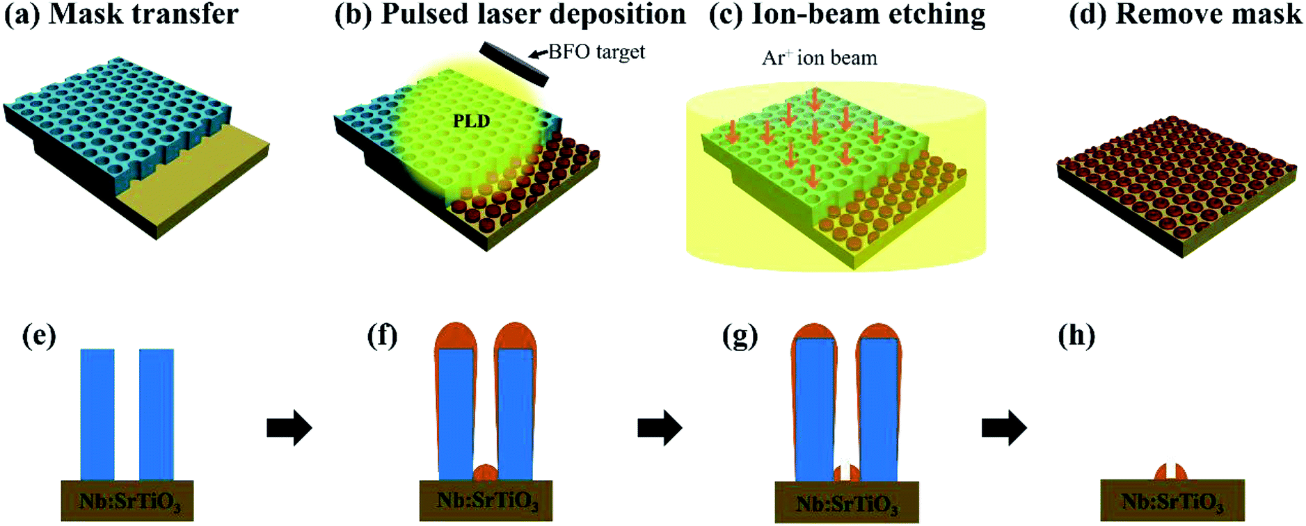 | ||
| Fig. 1 Schematic diagrams of the fabrication process of BFO nanorings. (a) AAO mask transferring; (b) synthesis of BFO nanodots by AAO-assisted pulsed laser deposition; (c) Ar ion-beam etching of BFO nanodots; (d) AAO mask removal; (e–h) the sketches of a single nanoring fabrication process. | ||
To illustrate the formation mechanism of BFO nanorings, the sketches of a single nanoring fabrication process are described in Fig. 1e–h, corresponding to Fig. 1a–d, respectively. The through-hole AAO template is taken as a mask to define nanodots as shown in Fig. 1e. PLD is used to fabricate BFO nanodots through the AAO mask as shown in Fig. 1f. It is worth to note that, during this PLD process, BFO is deposited both on the substrate and the pore walls. This is followed by Ar ion beam etching that produces the BFO nanoring due to the blocking of the deposited BFO on the walls, as shown in Fig. 1g. The redeposition of BFO nanodots inside the pore during the ion beam etching might help to form the nanoring as well. In the following step, after removal of the AAO template, a BFO nanoring is fabricated as presented in Fig. 1h.
Characterizations
Atomic force microscopy (AFM) and piezoresponse force microscopy (PFM) were measured using scanning probe microscope (Cypher Asylum research) with conducting Pt/Ir coated AFM probes (nanoworld). The crystal structures of the BFO films were characterized by X-ray diffraction (XRD, PANalytical X'Pert PRO). The microstructures were verified by transmission electron microscopy (TEM, JOEL-2011, 200 kV). AFM and plan-view TEM measurements were performed to study the topographies of the obtained BiFeO3 nanoring arrays. To demonstrate the epitaxial structure of the nanorings, XRD θ–2θ scan, reciprocal space mapping (RSM) and cross-sectional TEM were applied. The ferroelectric properties and polarization switching behaviors have also been revealed by PFM.Results and discussion
AFM measurements
The topography of the BFO nanoring array, captured by AFM, is shown Fig. 2a. It is revealed that well-ordered BFO nanorings are fabricated using this facile route. To better understand the fabrication process of BFO nanoring array, high-resolution 3D AFM images of the nanodot and nanoring topographies are shown in Fig. 2b and c. The AFM image in Fig. 2b shows the morphology of the sample after PLD growth (corresponding to Fig. 1b and f), demonstrating the formation of isolated BFO nanodots with diameters around 70 nm. Then, BFO nanorings are fabricated after ion beam etching (Fig. 1c and g) and AAO mask removal (Fig. 1d and h). The 3D AFM image in Fig. 3c further confirms the high quality of the isolated BFO nanorings. Combing the AFM image (Fig. 2c) with the cross-section line profile (Fig. 2d), it is found that the typical dimensions of the nanorings are 12 nm inner diameter with 30 nm wall thickness and heights around 10 nm. These results demonstrate the successful synthesis of ordered BFO nanoring array using this novel method. In addition, it is worth to note that size-tunable nanorings could be produced by using different sizes of AAO template. | ||
| Fig. 2 (a) The AFM topography image of a large scale BFO nanoring array; (b) the 3D AFM image of BFO nanodots after AAO-assisted PLD in Fig. 1b; (c) the 3D AFM image of the isolated BFO nanorings; (d) the cross-section line profile along the blue line in (c). | ||
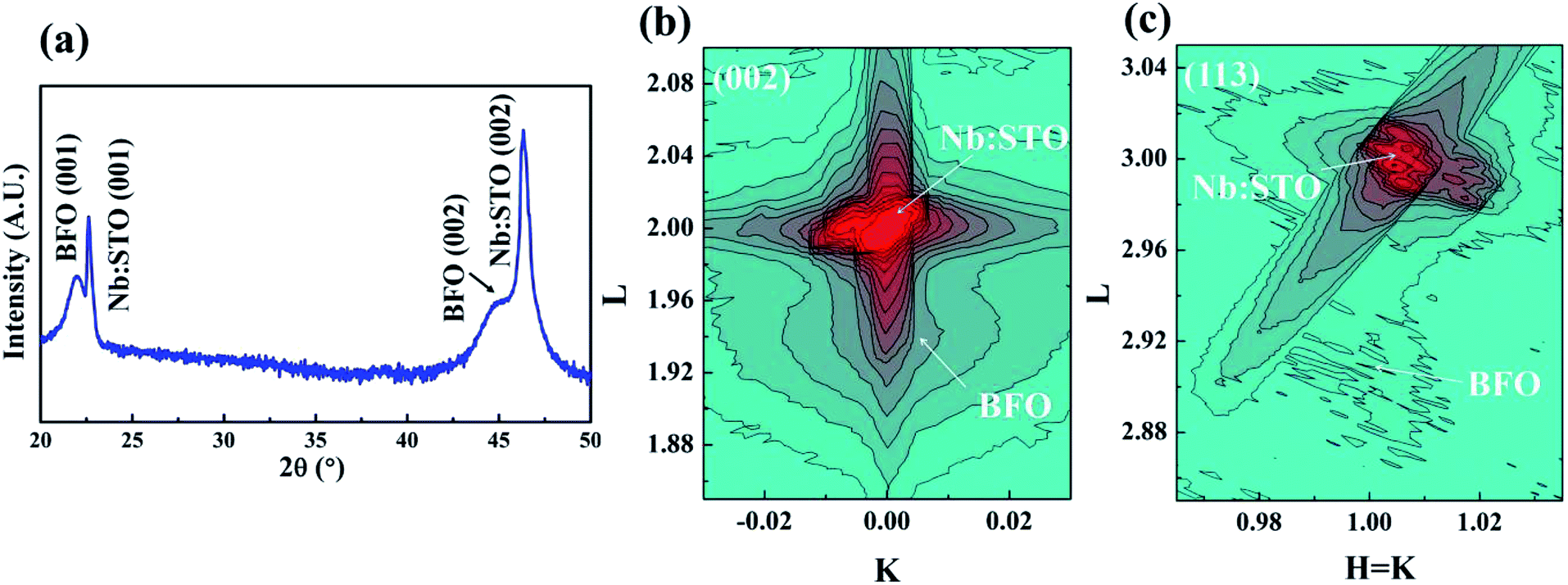 | ||
| Fig. 3 (a) X-ray diffraction θ–2θ scan; (b) (002) and (c) (113) reciprocal space mapping (RSM) of BFO nanoring array. | ||
XRD and RSM characterizations
The structure of the obtained BFO nanoring array is characterized by XRD as shown in Fig. 3. XRD θ–2θ scan shows the (002) diffraction peaks of BFO nanorings and the single crystal Nb:STO substrate (Fig. 3a), indicating the epitaxial structure the BFO nanorings. This is further confirmed by (002) and (103) RSM data shown in Fig. 3b and c. It is worth to mention that both the intensity of (002) and (103) peaks relative to BFO is weak because the thickness of the BFO nanoring sample is very thin and it is isolated nanoring array. To verify this, we measured the RSM data of both the BFO nanoring sample on Nb:STO and a bare Nb:STO substrate (not shown here). As expected, the peaks marked with BFO in Fig. 3b and c are from BFO nanorings, where no BFO peaks are found in the bare Nb:STO substrate. In addition, it is expected that BFO nanorings are fully strained with the Nb:STO substrate as the thickness (height) of the ring is very thin (∼10 nm). The in-plane and out-of-plane lattice constants of BFO nanodots are a ∼ 3.905 Å and c ∼ 4.02 Å according to the XRD θ–2θ scan and RSM data in Fig. 3, confirming the fully compressive strain imposed by the Nb:STO substrate (bulk BFO, a ∼ 3.96 Å; Nb:STO, a ∼ 3.905 Å).TEM and FFT measurements
The successful synthesis of BFO nanorings is also demonstrated by the plan-view TEM image of the nanoring array (Fig. 4a) and the cross-sectional TEM image of a single ring (Fig. 4b). It is also revealed, in Fig. 4a and b, that the dimensions of the rings are 12 nm inner diameter with 30 nm wall thickness and heights around 10 nm, which is in consistent with the AFM data in Fig. 2. The high-resolution TEM image of the left nanoring wall in Fig. 2b is shown in Fig. 2c, demonstrating the sharp interface between BFO and Nb:STO. The fast Fourier transformation (FFT) patterns of the red rectangle marked BFO region and blue rectangle marked Nb:STO region in Fig. 4c further reveal the epitaxial growth of BFO nanorings and the fully strain state (these data are in agreement with the XRD data in Fig. 3), which are shown in Fig. 4d and e, respectively. Thus, these results have verified the fabrication of high quality epitaxial BFO nanorings using AAO template-assisted pulsed laser deposition and ion beam etching method. | ||
| Fig. 4 (a) A plan-view TEM image of the obtained BFO nanoring array; (b) a cross-sectional TEM image of a single ring; (c) high-resolution TEM image showing sharp interfaces between the wall of BFO nanoring and Nb:STO substrate; fast Fourier transformation (FFT) patterns of (d) the red rectangle marked BFO region and (e) the blue rectangle marked Nb:STO region in (c). | ||
Characterizations of ferroelectric properties
We then turn to study the ferroelectric properties of the BFO nanoring array. The ferroelectric domain structures of these nanorings were characterized by PFM with a scanning probe mode (Asylum Research) using conductive PFM probes. The local piezoresponse loop measurements are carried out by fixing the PFM probe on a selected point of a nanoring and then applying a triangle square waveform accompanying with an ac driven voltage, via the conductive PFM probe. The vector PFM function of the AFM unit allows simultaneously mapping the vertical (out-of-plane) and lateral (in-plane) phase signals of the nanorings.The topography, vertical (out-of-plane) phase and lateral (in-plane) phase PFM images are presented in Fig. 5a–c. Dark contrast of the vertical PFM phase (Fig. 5b) indicates the polarization direction of the as prepared nanorings is upward. To exclude the possible cross-talk effects and demonstrate the ferroelectricity of these nanorings, the electrical switching study were conducted, as shown in Fig. 5d and e. The polarization direction is switched by applying a DC voltage of +5 V, while it does not change with −5 V, again revealing the upward polarization direction of the as prepared nanorings. Here we would like to mention that the relatively low conductivity of Nb:STO substrate leads to the imperfect switching of all nanorings with a voltage of +5 V. The retention properties of BFO nanorings were investigated as well, as shown in Fig. 5f. There is not obvious change of the vertical phase contrast after 24 h. In addition, the piezoresponse phase–voltage hysteresis (Fig. 5e) and butterfly-like amplitude–voltage loops (Fig. 5f) of three randomly selected nanorings in Fig. 5d are conducted. It is revealed that all the three phase loops are with 180° switching and the amplitude loops are butterfly-like. It is also found that the switching voltage of the nanorings is around 2.5 V. These results shown in Fig. 5 demonstrate the ferroelectricity and polarization reversal of the BFO nanoring array, which is promising for high-density non-volatile memory devices.
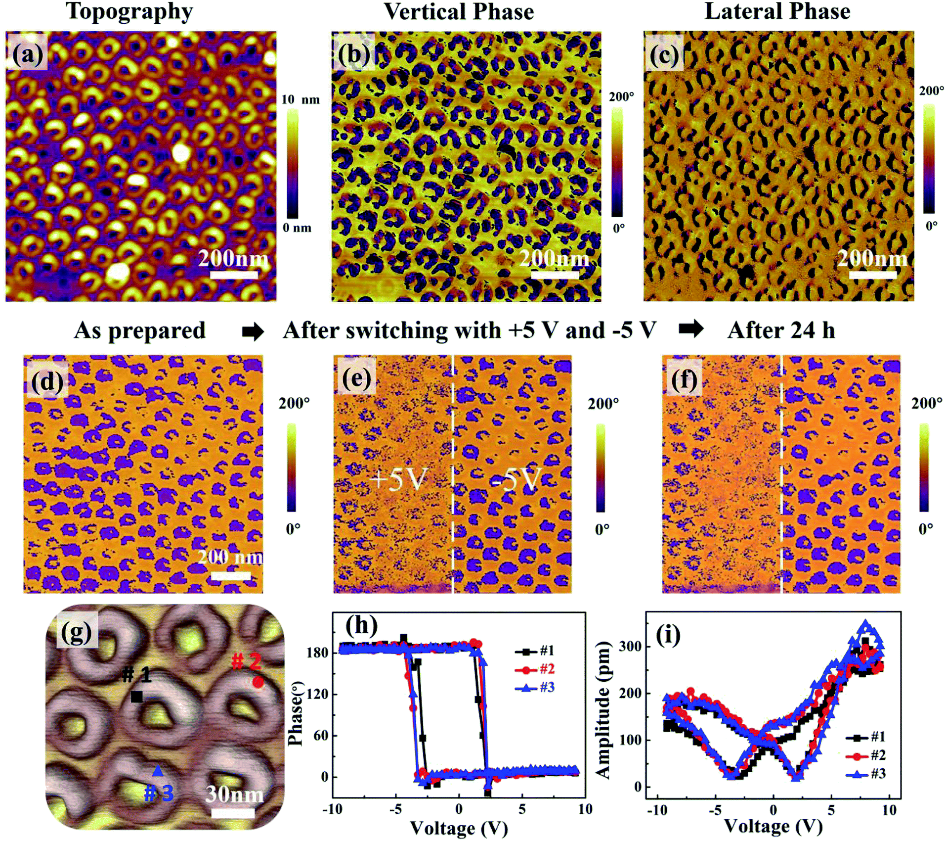 | ||
| Fig. 5 (a) Topography, (b) vertical (out-of-plane), and (c) lateral (in-plane) PFM phase images of BFO nanoring array; (d)–(f) vertical PFM phase images showing electrical switching and the retention properties of the nanorings: (d) as prepared state; (e) after switching with +5 V and −5 V DC voltage; (f) vertical phase images re-captured after 24 h; (g) a random selected 3D AFM topography image of the obtained BFO nanoring array; (h) the phase–voltage loops, and (i) butterfly-like amplitude–voltage loops of three randomly selected nanorings in (g). | ||
Conclusions
In summary, ordered BFO nanorings have been successfully fabricated using AAO template-assisted pulsed laser deposition and ion beam etching method. The typical dimensions of the BFO nanorings are 12 nm inner diameter with 30 nm wall thickness and heights around 10 nm. Moreover, the BFO nanoring array synthesized using this method maintains the epitaxial structure, strong ferroelectricity and polarization reversal, which is promising for high-density non-volatile memory devices. The dimensions of the nanorings could be tunable by using different sizes of AAO templates. Furthermore, the fabrication of BFO nanorings opens a pathway to study related new physical phenomena (such as ferroelectric vortices). This novel and facile approach could also be extended to other materials systems to fabricate nanorings (such as BaTiO3, ZnO and Au).Conflicts of interest
There are no conflicts to declare.Acknowledgements
The authors would like to thank the National Key Research Program of China (No. 2016YFA0201002), the State Key Program for Basic Researches of China (No. 2015CB921202), the Natural Science Foundation of China (No. 11674108, 51072061, 51272078, 51431006), the Project for Guangdong Province Universities and Colleges Pearl River Scholar Funded Scheme (2014), the Natural Science Foundation of Guangdong Province (No. 2016A030308019), and the Science and Technology Planning Project of Guangdong Province (No. 2015B090927006).Notes and references
- J. F. Scott, Nat. Mater., 2005, 4, 13–14 CrossRef CAS.
- J. F. Scott, Science, 2007, 315, 954–959 CrossRef CAS PubMed.
- D. Chen, X. Gao and J.-M. Liu, MRS Commun., 2016, 6, 330–340 CrossRef CAS.
- I. I. Naumov, L. Bellaiche and H. Fu, Nature, 2004, 432, 737–740 CrossRef CAS PubMed.
- G. Catalan, J. Seidel, R. Ramesh and J. F. Scott, Rev. Mod. Phys., 2012, 84, 119–156 CrossRef CAS.
- F.-T. Huang, B. Gao, J.-W. Kim, X. Luo, Y. Wang, M.-W. Chu, C.-K. Chang, H.-S. Sheu and S.-W. Cheong, npj Quantum Materials, 2016, 1, 16017 CrossRef.
- S. Prosandeev, I. I. Naumov, H. Fu, L. Bellaiche, M. P. D. Campbell, R. G. P. McQuaid, L.-W. Chang, A. Schilling, L. J. McGilly, A. Kumar and J. Marty Gregg, in Nanoscale Ferroelectrics and Multiferroics, John Wiley & Sons, Ltd, 2016, pp. 700–728 Search PubMed.
- H. Pang, F. Zhang, M. Zeng, X. Gao, M. Qin, X. Lu, J. Gao, J. Dai and Q. Li, npj Quantum Materials, 2016, 1, 16015 CrossRef.
- Y. L. Tang, Y. L. Zhu, X. L. Ma, A. Y. Borisevich, A. N. Morozovska, E. A. Eliseev, W. Y. Wang, Y. J. Wang, Y. B. Xu, Z. D. Zhang and S. J. Pennycook, Science, 2015, 348, 547–551 CrossRef CAS PubMed.
- A. K. Yadav, C. T. Nelson, S. L. Hsu, Z. Hong, J. D. Clarkson, C. M. Schlepüetz, A. R. Damodaran, P. Shafer, E. Arenholz, L. R. Dedon, D. Chen, A. Vishwanath, A. M. Minor, L. Q. Chen, J. F. Scott, L. W. Martin and R. Ramesh, Nature, 2016, 530, 198–201 CrossRef CAS PubMed.
- H. Han, Y. Kim, M. Alexe, D. Hesse and W. Lee, Adv. Mater., 2011, 23, 4599–4613 CrossRef CAS PubMed.
- S. R. Burns, J. M. Gregg and V. Nagarajan, Adv. Funct. Mater., 2016, 26, 8367–8381 CrossRef CAS.
- A. Schilling, D. Byrne, G. Catalan, K. G. Webber, Y. A. Genenko, G. S. Wu, J. F. Scott and J. M. Gregg, Nano Lett., 2009, 9, 3359–3364 CrossRef CAS PubMed.
- G. Tian, L. Zhao, Z. X. Lu, J. X. Yao, H. Fan, Z. Fan, Z. W. Li, P. L. Li, D. Y. Chen, X. Y. Zhang, M. H. Qin, M. Zeng, Z. Zhang, J. Y. Dai, X. S. Gao and J. M. Liu, Nanotechnology, 2016, 27, 485302 CrossRef PubMed.
- Y. Kim, Y. Kim, H. Han, S. Jesse, S. Hyun, W. Lee, S. V. Kalinin and J. K. Kim, J. Mater. Chem. C, 2013, 1, 5299–5302 RSC.
- H. Zheng, J. Wang, S. E. Lofland, Z. Ma, L. Mohaddes-Ardabili, T. Zhao, L. Salamanca-Riba, S. R. Shinde, S. B. Ogale, F. Bai, D. Viehland, Y. Jia, D. G. Schlom, M. Wuttig, A. Roytburd and R. Ramesh, Science, 2004, 303, 661–663 CrossRef CAS PubMed.
- S. Mohan and B. Subramanian, RSC Adv., 2013, 3, 23737–23744 RSC.
- D. Moitra, B. K. Ghosh, M. Chandel and N. N. Ghosh, RSC Adv., 2016, 6, 97941–97952 RSC.
- X. H. Zhu, P. R. Evans, D. Byrne, A. Schilling, C. Douglas, R. J. Pollard, R. M. Bowman, J. M. Gregg, F. D. Morrison and J. F. Scott, Appl. Phys. Lett., 2006, 89, 122913 CrossRef.
- W. Dong, B. Li, Y. Li, X. Wang, L. An, C. Li, B. Chen, G. Wang and Z. Shi, J. Phys. Chem. C, 2011, 115, 3918–3925 CAS.
- D. Byrne, A. Schilling, J. F. Scott and J. M. Gregg, Nanotechnology, 2008, 19, 165608 CrossRef CAS PubMed.
- H. Han, R. Ji, Y. J. Park, S. K. Lee, G. Le Rhun, M. Alexe, K. Nielsch, D. Hesse, U. Goesele and S. Baik, Nanotechnology, 2009, 20, 015301 CrossRef PubMed.
- W. H. Ma, D. Hesse and U. Gosele, Nanotechnology, 2006, 17, 2536–2541 CrossRef CAS PubMed.
- J. Wang, J. B. Neaton, H. Zheng, V. Nagarajan, S. B. Ogale, B. Liu, D. Viehland, V. Vaithyanathan, D. G. Schlom, U. V. Waghmare, N. A. Spaldin, K. M. Rabe, M. Wuttig and R. Ramesh, Science, 2003, 299, 1719–1722 CrossRef CAS PubMed.
- D. Chen, Z. Chen, Q. He, J. D. Clarkson, C. R. Serrao, A. K. Yadav, M. E. Nowakowski, Z. Fan, L. You, X. Gao, D. Zeng, L. Chen, A. Y. Borisevich, S. Salahuddin, J.-M. Liu and J. Bokor, Nano Lett., 2017, 17, 486–493 CrossRef CAS PubMed.
- J. Seidel, L. W. Martin, Q. He, Q. Zhan, Y. H. Chu, A. Rother, M. E. Hawkridge, P. Maksymovych, P. Yu, M. Gajek, N. Balke, S. V. Kalinin, S. Gemming, F. Wang, G. Catalan, J. F. Scott, N. A. Spaldin, J. Orenstein and R. Ramesh, Nat. Mater., 2009, 8, 229–234 CrossRef CAS PubMed.
- S. Y. Yang, J. Seidel, S. J. Byrnes, P. Shafer, C. H. Yang, M. D. Rossell, P. Yu, Y. H. Chu, J. F. Scott, J. W. Ager III, L. W. Martin and R. Ramesh, Nat. Nanotechnol., 2010, 5, 143–147 CrossRef CAS PubMed.
- R. J. Zeches, M. D. Rossell, J. X. Zhang, A. J. Hatt, Q. He, C. H. Yang, A. Kumar, C. H. Wang, A. Melville, C. Adamo, G. Sheng, Y. H. Chu, J. F. Ihlefeld, R. Erni, C. Ederer, V. Gopalan, L. Q. Chen, D. G. Schlom, N. A. Spaldin, L. W. Martin and R. Ramesh, Science, 2009, 326, 977–980 CrossRef CAS PubMed.
- D. Chen, C. T. Nelson, X. Zhu, C. R. Serrao, J. D. Clarkson, Z. Wang, Y. Gao, S.-L. Hsu, L. R. Dedon, Z. Chen, D. Yi, H.-J. Liu, D. Zeng, Y.-H. Chu, J. Liu, D. G. Schlom and R. Ramesh, Nano Lett., 2017 DOI:10.1021/acs.nanolett.7b03030.
- C. Huang and L. Chen, Materials, 2014, 7, 5403–5426 CrossRef CAS PubMed.
- J. G. Wu, Z. Fan, D. Q. Xiao, J. G. Zhu and J. Wang, Prog. Mater. Sci., 2016, 84, 335–402 CrossRef CAS.
- Z. Chen, J. Liu, Y. Qi, D. Chen, S.-L. Hsu, A. R. Damodaran, X. He, A. T. N'Diaye, A. Rockett and L. W. Martin, Nano Lett., 2015, 15, 6506–6513 CrossRef CAS PubMed.
- S. Dong, J.-M. Liu, S.-W. Cheong and Z. Ren, Adv. Phys., 2015, 64, 519–626 CrossRef CAS.
- J. T. Heron, J. L. Bosse, Q. He, Y. Gao, M. Trassin, L. Ye, J. D. Clarkson, C. Wang, J. Liu, S. Salahuddin, D. C. Ralph, D. G. Schlom, J. Iniguez, B. D. Huey and R. Ramesh, Nature, 2014, 516, 370–373 CrossRef CAS PubMed.
- G. Catalan, H. Bea, S. Fusil, M. Bibes, P. Paruch, A. Barthelemy and J. F. Scott, Phys. Rev. Lett., 2008, 100, 027602 CrossRef CAS PubMed.
- A. Lubk, S. Gemming and N. A. Spaldin, Phys. Rev. B, 2009, 80, 104110 CrossRef.
- N. Balke, S. Choudhury, S. Jesse, M. Huijben, Y. H. Chu, A. P. Baddorf, L. Q. Chen, R. Ramesh and S. V. Kalinin, Nat. Nanotechnol., 2009, 4, 868–875 CrossRef CAS PubMed.
- C. T. Nelson, B. Winchester, Y. Zhang, S.-J. Kim, A. Melville, C. Adamo, C. M. Folkman, S.-H. Baek, C.-B. Eom, D. G. Schlom, L.-Q. Chen and X. Pan, Nano Lett., 2011, 11, 828–834 CrossRef CAS PubMed.
| This journal is © The Royal Society of Chemistry 2017 |