DOI:
10.1039/C7RA07640A
(Paper)
RSC Adv., 2017,
7, 42455-42461
Electronic and excitonic properties of two-dimensional and bulk InN crystals
Received
11th July 2017
, Accepted 24th August 2017
First published on 1st September 2017
Abstract
Motivated by potential extensive applications in nanoelectronics devices of III–V materials, we calculate the structural and optoelectronic properties of two-dimensional (2D) InN as well as its three-dimensional (3D) counterparts by using density functional theory (DFT). Compared with the 3D form, the In–N bonding in the 2D InN layer is stronger in terms of the shorter bond length, and the formation of the 2D one is higher in terms of the lower cohesive energy. The bandgap of monolayer InN is 0.31 eV at PBE level and 2.02 eV at GW0 level. By many-body GW0 and BSE within RPA calculations, monolayer InN presents an exciton binding energy of 0.12 eV. The fundamental bandgap increases along with layer reduction and is converted from direct (0.7–0.9 eV) in bulk InN to indirect (2.02 eV) in monolayer InN. Under biaxial compressive strain, the bandgap of 2D-InN can be further tuned from indirect to direct.
1. Introduction
Since the discovery of graphene,1,2 2D materials have attracted great interest due to their large surface area and unusual mechanical, electronic and optical properties.3–13 These novel properties make the 2D materials promising for applications in photocatalysis, nanoelectronic devices, energy storage, thermal conductors and even topological insulators. The III–V materials, in their bulk form developed over a rather long time, have also joined the 2D materials family. Boron-nitride (BN) sheets have the same planar honeycomb structure as graphene, and their ionic character causes an energy gap of 4.64 eV at the K point.2 Layered hexagonal AlN, which was experimentally realized by Tsipas et al.14 recently, displays transparent features in the visible light range. Monolayer honeycomb structured GaN, even if at high temperature, can remain stable, confirmed by high-temperature ab initio molecular-dynamics simulations.15 The experimental realization of 2D materials by chemical vapor deposition and molecular beam epitaxy, etc, requires suitable substrates. A. K. Singh et al.16 theoretically predicts that several transition-metal and rare-earth-metal substrates can be used to synthesize and stabilize 2D hexagonal III–V materials.
Among III–V materials, bulk InN has a less than 1.0 eV direct bandgap which could be suitable for low-bandgap device applications such as future-generation solar cells because the nitride alloys can cover the whole solar spectrum range.17 Doping other III or V element into the host could achieve an extent potential application prospect in optoelectronic and high power/temperature electronic devices including light emitting diodes (LEDs), laser diodes (LDs), solar blind photodetectors and heterostructure field effect transistors.18–21 2D materials display different properties from their 3D counterparts, and the knowledge of the 3D form cannot be directly delivered to the 2D one. To the best of our knowledge, the studies on the 2D-InN are rare and most of them are focused on the geometry, growth dynamics, and intrinsic electronic properties of monolayers. The optical properties, and the modification of optoelectronic properties of 2D-InN, which are of great importance for potential nanoelectronic and optical applications, remain open.
In this study, the mechanical, stability, electronic and optical properties of bulk and 2D hexagonal planar InN based on density functional theory (DFT) are investigated to elucidate the difference between bulk and 2D structure, to determine the effect of strain on bandgap of 2D-InN as well as the bandgap variation of bilayer and multilayer structures (include van der Waals). Besides, by many-body calculations, exciton binding energy of 2D-InN is also obtained. The paper is organized as follows. In Section 2, we describe details of computational methods. The results and discussions are provided in Section 3. Finally, a brief summary is summarized in Section 4.
2. Methods and computational details
All the theoretical calculations are carried out by using DFT22 of the projector augmented wave method (PAW)23,24 as implemented in the Vienna ab initio simulation package (VASP).25 The exchange-correlation potential is in the form of generalized gradient approximation (GGA) of the Perdew–Burke–Ernzerhof (PBE).26 The plane-wave basis set is defined by an energy cutoff of 520 eV for all calculations. The structural optimization is allowed to relax until the maximum force on each atom becomes less than 0.001 eV Å−1 and maximum energy change between two steps is smaller than 10−6 eV. The Γ-centered 7 × 7 × 7 and 12 × 12 × 1 K-point meshes are used in the first Brillouin zone for 3D and 2D InN respectively. The height of each unit cell of 2D InN is maintained at 20 Å to eliminate the interaction between periodic images of slabs in z-direction. The van der Waals interactions that have a significant role on layered materials are taken into account for the multilayered structures.27,28
In order to overcome the bandgap problem of GGA potential, we employ HSE06![[thin space (1/6-em)]](https://www.rsc.org/images/entities/char_2009.gif) 29 and quasiparticle (QP) GW0 corrections,30–32 because of their accuracy in describing the electronic structures of semiconductors and insulators. Regarding the optical response calculations, the random phase approximation (RPA)33,34 is undertaken on top of HSE06 and GW0 approaches. The attraction between quasi-electron and hole (on top of GW0 approximation) by solving BSE35,36 is taken into account. A unified K-point mesh 36 × 36 × 1 is adopted for the GW0 and BSE methods, which is enough for BSE calculation. The total number of empty bands is 336 used for the GW0 calculations. The six highest valence bands and the eight lowest conduction bands are included as basis for the excitonic state. BSE is solved using the Tamm–Dancoff approximation.
29 and quasiparticle (QP) GW0 corrections,30–32 because of their accuracy in describing the electronic structures of semiconductors and insulators. Regarding the optical response calculations, the random phase approximation (RPA)33,34 is undertaken on top of HSE06 and GW0 approaches. The attraction between quasi-electron and hole (on top of GW0 approximation) by solving BSE35,36 is taken into account. A unified K-point mesh 36 × 36 × 1 is adopted for the GW0 and BSE methods, which is enough for BSE calculation. The total number of empty bands is 336 used for the GW0 calculations. The six highest valence bands and the eight lowest conduction bands are included as basis for the excitonic state. BSE is solved using the Tamm–Dancoff approximation.
3. Results and discussions
3.1 3D InN crystals
We carry out structure optimization and electronic structures calculations of wurtzite (wz) and zinc-blende (zb) InN crystals with GGA-PBE and HSE06 potentials, respectively. The equilibrium lattice constants, In–N bond length d, cohesive energy per In–N pair Ec, bulk modulus B and direct bandgap EΓ–Γ of wz and zb-InN are presented in Table 1 and Table 2, together with other theoretical and experimental data. The present calculations predict a = 3.62 Å, c = 5.83 Å for wz-InN, the c/a ratio is 1.61, which are in good agreement with previous GGA calculations of a = 3.61, 3.55 Å and c = 5.88, 5.73 Å, while slightly larger than those of LDA calculations, a = 3.54, 3.53 Å and c = 5.76, 5.54 Å.37,38 With respect to experimental values of a = 3.53 Å and c = 5.69 Å,41–45 the calculated results are large by 2.55% and 2.46% respectively. And the measured bond length of In–N is 2.21 Å. Here, the cohesive energy per In–N pair (Ec) can be given by,| | |
Ec = E(In) + E(N) − E(InN)
| (1) |
where E(In) and E(N) represent the energies of free In and N atoms and E(InN) is the optimized total energy of InN. The higher the positive Ec, the stronger is the binding. The experimentally measured Ec is 7.97 eV,41–45 our obtained value is 10.12 eV. Meanwhile there are some other theoretical results of 8.69 and 6.87 eV. In addition, the predicted bulk modulus is 82.04 GPa, which is lower than the experimental values of 125 GPa.
Table 1 Lattice constants a = b and c, c/a ratio, bond length d, cohesive energy per In–N pair Ec, bulk modulus B, and direct bandgap EΓ–Γ of wz-InN crystal calculated by using PBE and HSE06 approaches. For the sake of comparison, values obtained from the previous theoretical studies and experiments are also included
| |
a (Å) |
c (Å) |
c/a |
d (Å) |
Ec (eV/InN) |
B (GPa) |
Eg (eV) |
| PBE/HSE06 |
3.62 |
5.83 |
1.61 |
2.21 |
10.12 |
82.04 |
0/0.50 |
| LDA37,38 |
3.54, 3.53 |
5.76, 5, 54 |
1.62, 1.57 |
|
8.69 |
140, 146.2 |
0.27, 0.017 |
| GGA37,38 |
3.61, 3.55 |
5.88, 5.73 |
1.63, 1.61 |
|
6.87 |
116.1, 121.58 |
0.37, 0.029 |
| mBJ38 |
|
|
|
|
|
|
0.399 |
| HSE39,40 |
|
|
|
|
|
|
0.57, 0.68 |
| Expt.41–45 |
3.53 |
5.69 |
1.61 |
|
7.97 |
125 |
0.78–0.90 |
Table 2 Lattice constants a = b = c, bond length d, cohesive energy per In–N pair Ec, bulk modulus B, and direct bandgap EΓ–Γ of zb-InN crystal calculated by using PBE and HSE06 approaches. For the sake of comparison, previous theoretical results and experiments are also included
| |
a (Å) |
d (Å) |
Ec (eV/InN) |
B (GPa) |
Eg (eV) |
| PBE/HSE06 |
5.10 |
2.21 |
9.57 |
97.74 |
0/0.30 |
| LDA37,38 |
5.00, 4.94 |
|
8.67 |
140, 147.24 |
−0.40, 0 |
| GGA37,38 |
5.11, 5.04 |
|
6.85 |
116.96, 122.10 |
−0.55, 0 |
| EV-GGA38 |
|
|
|
|
0.53 |
| mBJ38 |
|
|
|
|
0.73 |
| Expt.43–47 |
4.98 |
|
|
137 |
0.70–0.90 |
As for zb-InN, the lattice constant obtained from previous theoretical result is between 4.94 and 5.11 Å37,38 and is predicted here as 5.10 Å, which is 2.41% larger than experimental value of 4.98 Å.43–47 The equivalent In–N bond length is 2.21 Å. The cohesive energy per In–N pair calculated as Ec = 9.57 eV is slightly smaller than that of wz-InN because thermodynamically stable phase of 3D InN crystal has a wurtzite structure, which corresponds to a global minimum. Furthermore, the bulk modulus of 97.74 GPa is smaller than experimental value of 137 GPa.
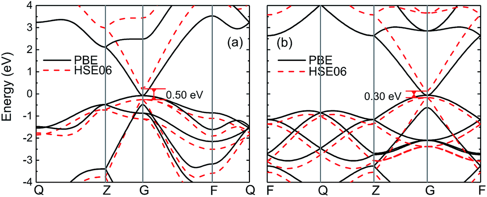
Fig. 1 shows the band structures of wz and zb-InN crystals obtained by using PBE and HSE06 methods. The energy bands of wz-InN calculated by PBE predict a near zero bandgap, which is largely underestimated with respect to the reported experimental values of 0.78–0.9 eV.41–45 With corrections by using HSE06, the direct bandgap increases to 0.50 eV, while it maintains 0.28 eV below the experimental value. Similar to wz structure, as shown in Fig. 1(b), zb-InN exhibits a near zero bandgap with PBE. After HSE06 corrections, it has a direct bandgap 0.30 eV, which is still 0.40 eV smaller than experimentally measured value. Our prediction agrees with the previous calculations within PBE and HSE corrections.37–40
 |
| | Fig. 1 The electronic band structures of (a) wz and (b) zb-InN are obtained by using PBE (black solid curve) and HSE06 (red dashed curve) methods, respectively. The direct band gap EΓ–Γ by HSE06 is indicated. | |
3.2 2D InN
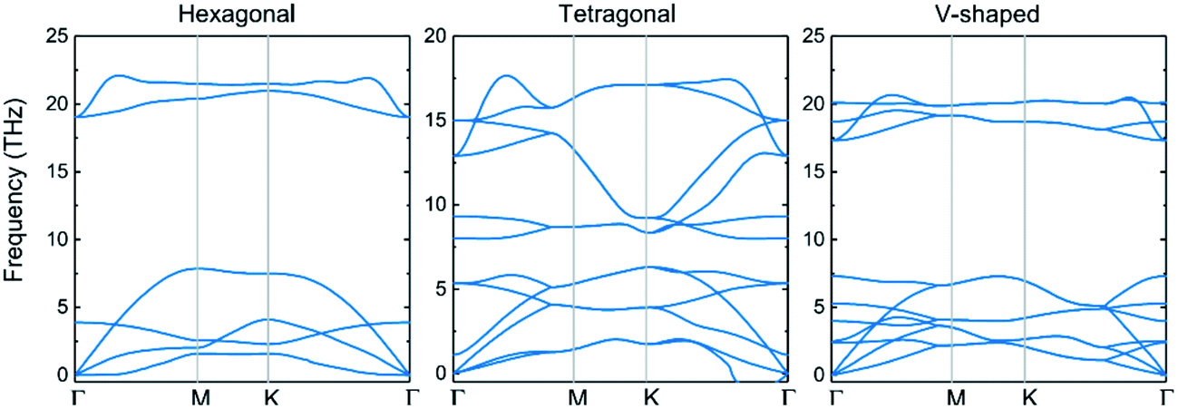
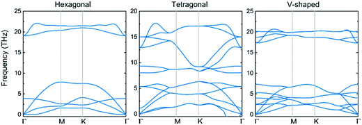
3.2.1 Stability and geometry-based properties. To provide a consistent comparison with 3D crystals to reveal the effect of dimensionality, we first establish three possible structures of 2D-InN, which are hexagonal (H), tetragonal (T) and V-shaped (V) structures, as shown in Fig. 2. The H structure (Fig. 2(a)) has the space group P![[6 with combining macron]](https://www.rsc.org/images/entities/char_0036_0304.gif) M2 and of which the orbital hybridization is sp2. The T structure (Fig. 2(b)) has the space group P4/NMM, unlike the threefold coordinated planar hexagonal structure, each cation and anion in the T structure is bonded to four neighboring anions and cations, respectively.48 The V structure (Fig. 2(c)) with the space group PMN21, which has inequilateral hexagonal rings from the top view. The orbital hybridization in the V structure is neither sp2 nor sp3. In order to determine the dynamical stability of each structure, the phonon spectra are calculated in Fig. 3. For the T and V structures, there exist imaginary frequency in the calculated frequencies of phonon modes, which reveal instability. The phonon dispersions of H structure are positive and indicate stability, which are similar to previous calculated results.48–50
M2 and of which the orbital hybridization is sp2. The T structure (Fig. 2(b)) has the space group P4/NMM, unlike the threefold coordinated planar hexagonal structure, each cation and anion in the T structure is bonded to four neighboring anions and cations, respectively.48 The V structure (Fig. 2(c)) with the space group PMN21, which has inequilateral hexagonal rings from the top view. The orbital hybridization in the V structure is neither sp2 nor sp3. In order to determine the dynamical stability of each structure, the phonon spectra are calculated in Fig. 3. For the T and V structures, there exist imaginary frequency in the calculated frequencies of phonon modes, which reveal instability. The phonon dispersions of H structure are positive and indicate stability, which are similar to previous calculated results.48–50
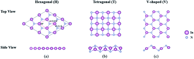 |
| | Fig. 2 The schematic diagram of (a) hexagonal, (b) tetragonal and (c) V-shaped 2D-InN structures from the top and side views, respectively. The hexagonal primitive unit cell is delineated by dashed lines. The lattice constants, bond angle between In–N bonds and In–N bond length are indicated. | |
 |
| | Fig. 3 Calculated phonon-dispersion curves of hexagonal, tetragonal and V-shaped structures, Γ versus K, along major symmetry directions of the Brillouin zone. | |
For optimized H structure, hybrid orbitals of In-sp2 and N-sp2 form σ-bonds along In–N bonds arranged as a hexagon. Due to the planar sp2 bonding, the bond angle between In–N bonds is 120°. In addition to three sp2 hybrid orbitals of each constituent, In and N, their pz orbitals are perpendicular to the plane of InN. While the σ-bonds attain the strength of InN, the π-bonds between nearest In-pz and N-pz orbitals maintain the planar geometry of InN.15 The optimized atomic structure and its lattice constant a, bond length d, cohesive energy Ec and minimum value of the energy gap, Eg calculated by using PBE, HSE06 and GW0 together with previous theoretical results are shown in Fig. 2(a) and Table 3. Our calculations predict a = 3.63 Å, which agrees well with previous values.48,49 The In–N bond of 2D-InN constructs from planar sp2 hybrid orbitals and pz orbitals, the value here we obtain is 2.10 Å, which is 0.11 Å shorter than the In–N bond of 3D wz(zb)-InN constructed from tetrahedrally coordinated sp3 hybrid orbitals. This indicates that In–N bonds in 2D-InN are stronger than those in wz(zb)-InN. Despite the stronger bonding in planar InN, the cohesive energy of 3D wz-InN crystal is 0.72 eV higher than that of 2D-InN (Ec = 9.40 eV).
Table 3 Lattice constant a, bond length d, cohesive energy Ec, minimum value of the energy gap, Eg calculated by using PBE, HSE06 and GW0. Previous theoretical values are also included
| |
a (Å) |
d (Å) |
Ec (eV) |
Eg (eV) |
| PBE/HSE06/GW0 |
3.63 |
2.10 |
9.40 |
0.31/1.48/2.02 (ΓK) |
| PBE/HSE06/G0W0 (ref. 48) |
3.63 |
|
|
—/1.52 (ΓK)/1.57 (ΓK) |
| LDA/GW0 (ref. 49) |
3.57 |
2.06 |
10.93 |
0.62 (ΓK)/5.76 (ΓΓ) |
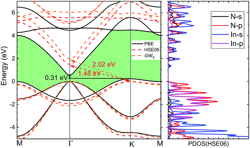
3.2.2 Electronic properties. Fig. 4 shows the band structures from PBE, HSE06 hybrid functional and GW0 method and Table 3 compares the bandgaps with present theoretical values. The valence band maximum (VBM) occurs at the K point, whereas the conduction band minimum (CBM) appears at the Γ point. Accordingly, the energy bands calculated by PBE predict an indirect bandgap EΓ–K = 0.31 eV. With corrections by using HSE06 and GW0 methods, indirect bandgap increases by 1.17 and 1.71 eV respectively. This is different from corresponding 3D wz(zb)-InN crystals, which have a near zero bandgap by PBE and a direct bandgap (0.50 eV) for wz and 0.30 eV for zb by HSE06. Obviously, the fundamental bandgap increases along with dimensionality reduction and is converted from direct to indirect, as the same of GaN.15 From the partial density of states (PDOS) by HSE06, we can note that the VBM is mainly from the N-p states together with certain contributions from the In-p states, while the CBM is dominated by the In-s states hybridization with the N-s states.
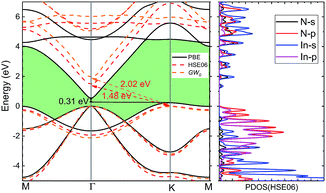 |
| | Fig. 4 The electronic band structure of monolayer InN is obtained by using PBE, HSE06 hybrid functional and GW0 method and indirect bandgap EΓ–K is indicated. The corresponding partial density of states (HSE06) is given in right side. | |
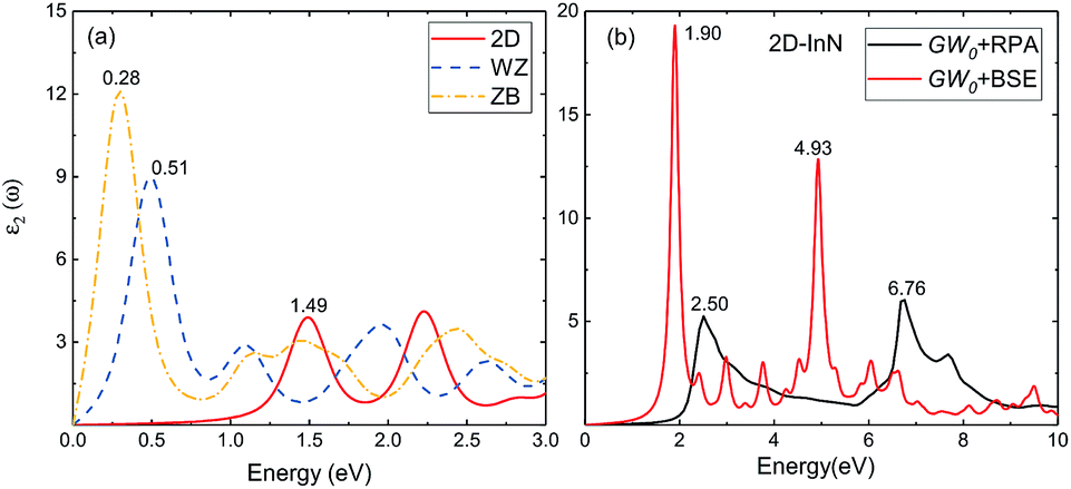
3.2.3 Optical properties. We use HSE06 functional and quasiparticle GW0 corrections within RPA to obtain the optical absorption energy. The electron–hole (e–h) interactions are taken into account by solving the BSE. In Fig. 5(a), we show imaginary part of the dielectric function for 2D, bulk wz and zb-InN, all the calculations using HSE06-RPA. The first absorption peak of 2D-InN is at 1.49 eV within near-infrared regime, which yields a blueshift compared to wz and zb-InN with the first absorption peak at 0.51 and 0.28 eV respectively. There is another single distinct peak at 2.23 eV. WZ-InN displays similar features that three peaks around 1.10, 1.93 and 2.64 eV. ZB-InN shows a broadened absorption phenomenon, leading to multipeaks, occurring in the vicinity of 1.4 and 2.4 eV. The oscillator strengths of major peaks in 2D-InN are evidently lower than those of wz(zb)-InN due to weaker linear optical response of a single-layer InN. Bulk wz(zb)-InN crystals are periodically repeated multiples of buckled InN planes along z direction. Hence, the optical spectra of monolayer and bulk InN show significant differences, indicating that they could be used for different optoelectronic applications.51
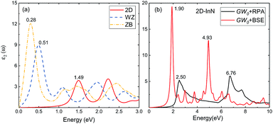 |
| | Fig. 5 Imaginary part of the dielectric function (a) for 2D-, bulk wz- and zb-InN using HSE06-RPA, (b) for 2D-InN using GW0 corrections with electron–hole interactions taken into account, together with GW0-RPA spectrum. | |
The absorption spectrum of 2D-InN given by GW0-BSE calculation is displayed in Fig. 5(b), together with GW0-RPA spectrum. We can obtain that the oscillator strengths of these peaks are enhanced considerably with electron–hole interactions taken into account. Under the quasiparticle direct bandgap (2.02 eV), there is a very significant light absorption peak (1.90 eV). This result is substantially dominated by the excitonic effect, due to the e–h interactions stemming from weak screening in low-dimensional InN. Comparing the lower GW0-BSE peak with quasiparticle bandgap excitation indicates the exciton binding energy is 0.12 eV, which is apparently higher than that of its wurtzite bulk structure (25 meV).52 The strongly bound excitons underline that for 2D-InN, e–h interaction can be significant to enhance the optical features in the absorption spectrum. The exciton effect is slightly weaker than that of other two-dimensional III–V materials, such as 1.7 eV in AlN monolayer honeycomb.51
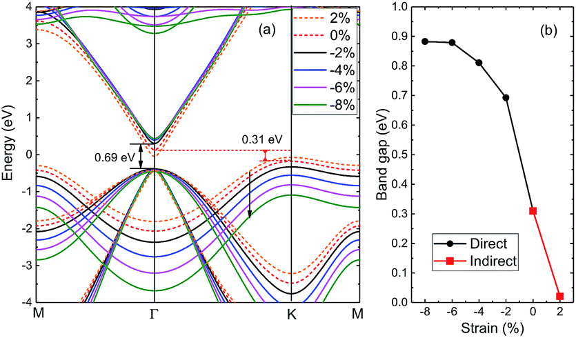
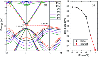
3.2.4 Strain effects. Strain has remarkable effect in tailoring electronic, and tunable electronic properties of 2D materials are crucial for their applications in optoelectronics. Here we examine the effect of strain on the fundamental bandgap of 2D-InN within PBE. Fig. 6 shows the values of bandgaps as a function of applied strain in the range of −8% to 2%. The positive and negative values of strain correspond to lattice expansion and compression, respectively. The bandgap of monolayer InN decreases under biaxial tensile strain, while it still remains an indirect semiconductor. When a biaxial compressive strain is exerted, monolayer InN converts from an indirect to direct bandgap. The bandgap increases to 0.69 eV at a −2% strain and continuously increases from 0.69 to 0.89 eV as strain up to −6%. Nevertheless, the further increase of strain up to −8% doesn't change the gap much. This variation is analogous to BN.53 Our calculations demonstrate that the bandgap of monolayer InN is sensitive to the biaxial strain, and exists an indirect to direct transition point, which is promising for optoelectronic applications due to their tunable bandgaps. Furthermore, those results would give a guild to find a suitable substrate.
 |
| | Fig. 6 (a) Variation of the energy bands of 2D-InN under applied biaxial strain. (b) Computed electronic bandgaps versus the biaxial strain ranging from −8% to 2%. | |
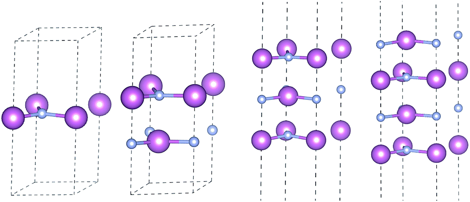
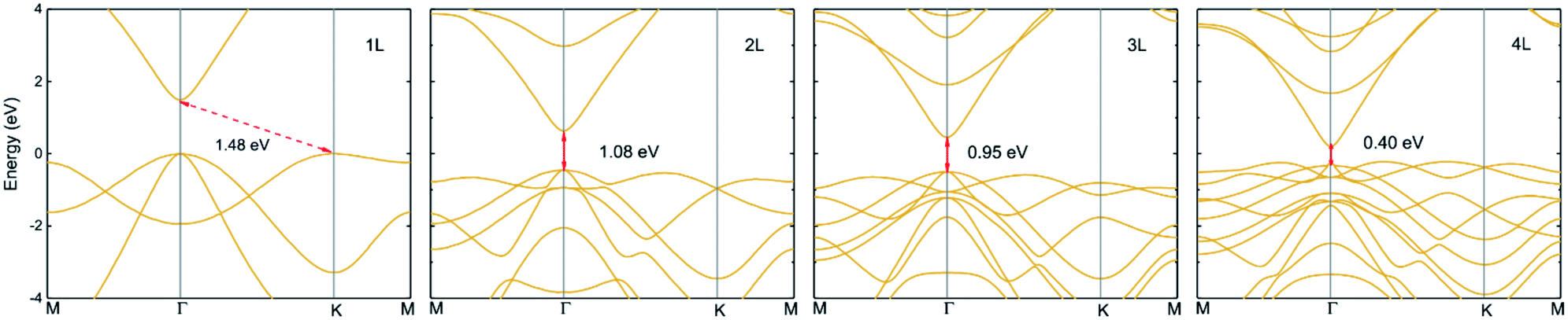
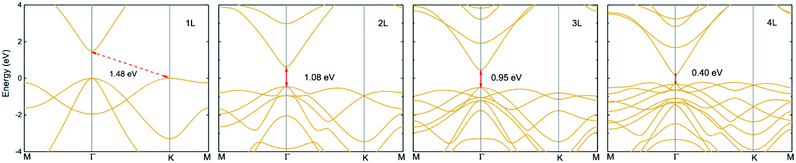
3.2.5 Layer dependence. Previous investigation shows thickness of two-dimensional materials has a significant effect in electronic properties. We explore this aspect of 2D-InN up to four layers and reveal its properties within HSE06 potential. The optimized structures for monolayer, bilayer, trilayer and four-layered InN are shown in Fig. 7, where the stacking sequences is hexagons on top of each other, with the In atom being above N.
 |
| | Fig. 7 Optimized atomic configuration for monolayer, bilayer, trilayer and four-layered InN. | |
 |
| | Fig. 8 Electronic band structures of monolayer, bilayer, trilayer and four-layered InN within HSE06 potential. The fundamental bandgaps are shown by arrows. | |
The lattice constant and bond length have no significant change with increasing layer up to three layers, an increase is found in four-layered InN, as listed in Table 4. However, interlayer distance and minimum bandgap display the different trend that they decrease with increasing layers, since interlayer interaction increases. The fundamental bandgap which is shown in Fig. 8 decreases from 1.48 eV to 1.08 eV in bilayer, to 0.95 eV in trilayer and to 0.40 eV in four-layered, these bandgaps are direct. There exists a crossover from indirect to direct in multilayered InN. Our calculations give a trend of band structure evolution with layers and the results shown here indicate rapid bandgap reduction. It indicates that the optoelectronic properties of layered 2D-InN can be controlled and tuned by modifying their structures.
Table 4 Lattice constants a, bond length d, interlayer distance h and fundamental bandgap Eg of monolayer, bilayer, trilayer and four-layered InN
| Layer |
a (Å) |
d (Å) |
h (Å) |
Eg (eV) |
| 1 |
3.63 |
2.10 |
— |
1.48 |
| 2 |
3.64 |
2.10 |
2.67 |
1.08 |
| 3 |
3.64 |
2.10 |
2.66/2.78 |
0.95 |
| 4 |
3.84 |
2.21 |
2.56/2.58/2.48 |
0.40 |
4. Conclusions
We perform mechanical, electronic and optical properties of monolayer and few layers 2D-InN as well as 3D counterparts based on density functional theory. The In–N bond of 2D-InN is 0.11 Å shorter than that of 3D wz(zb)-InN indicating stronger bonding, despite the stronger bonding in planar InN, 3D wz-InN crystal has a higher cohesive energy. Going from 3D to 2D InN, the bandgap increases and is converted from direct to indirect. In optical properties, the absorption spectrum yields a blueshift compared to (wz)zb-InN. By many-body calculations, 2D-InN presents an exciton binding energy of 0.12 eV. When a biaxial compressive strain is exerted, monolayer InN changes from an indirect to direct semiconductor, which is promising for optoelectronic applications due to their tunable bandgaps. Finally, we investigate the bandgap variation of bilayer and multilayer structures (include van der Waals) that decreases from 1.48 eV to 0.40 eV in four-layered InN, these bandgaps are direct. This indicates that the optoelectronic properties of layered 2D-InN can be controlled and tuned by modifying their structures.
Conflicts of interest
The authors declare no competing financial interests.
Acknowledgements
This work was supported by the National Natural Science Foundation of China (NO.61675032, 61671085), the National Key Research and Development Program of China (No. 2017YFB0405100), National Basic Research Program of China (973 Program) under Grant No. 2014CB643900, the Open Program of State Key Laboratory of Functional Materials for Informatics. We acknowledge the computational support from the Beijing Computational Science Research Center (CSRC).
References
- K. S. Novoselov, A. K. Geim, S. V. Morozov, D. Jiang, Y. Zhang, S. V. Dubonos, I. V. Grigorieva and A. A. Firsov, Science, 2004, 306, 666–669 CrossRef CAS PubMed
 .
. - K. S. Novoselov, D. Jiang, F. Schedin, T. J. Booth, V. V. Khotkevich, S. V. Morozov and A. K. Geim, Proc. Natl. Acad. Sci. U. S. A., 2005, 102, 10451–10453 CrossRef CAS PubMed .
- D. Liang, H. He, P. F. Lu, L. Y. Wu, C. F. Zhang, P. F. Guan and S. M. Wang, J. Mater. Sci., 2017, 52, 5799–5806 CrossRef CAS .
- K. F. Mak, C. Lee, J. Hone, J. Shan and T. F. Heinz, Phys. Rev. Lett., 2010, 105, 136805 CrossRef PubMed .
- H. He, P. F. Lu, L. Y. Wu, C. F. Zhang, Y. X. Song, P. F. Guan and S. M. Wang, Nanoscale Res. Lett., 2016, 11, 330 CrossRef PubMed .
- P. F. Lu, L. Y. Wu, C. H. Yang, D. Liang, R. G. Quhe, P. F. Guan and S. M. Wang, Sci. Rep., 2017, 7, 3912 CrossRef PubMed .
- Y. W. Zhu, S. Murali, M. D. Stoller, K. J. Ganesh, W. W. Cai, P. J. Ferreira, A. Pirkle, R. M. Wallace, K. A. Cychosz, M. Thommes, D. Su, E. A. Stach and R. S. Ruoff, Science, 2011, 332, 1537–1541 CrossRef CAS PubMed .
- J. Dai, Z. Y. Li, J. L. Yang and J. G. Hou, Nanoscale, 2012, 4, 3032–3035 RSC .
- L. Y. Wu, P. F. Lu, J. Y. Bi, C. H. Yang, Y. X. Song, P. F. Guan and S. M. Wang, Nanoscale Res. Lett., 2016, 11, 525 CrossRef PubMed .
- J. Feng, X. Sun, C. Z. Wu, L. L. Peng, C. W. Lin, S. L. Hu, J. L. Yang and Y. Xie, J. Am. Chem. Soc., 2011, 133, 17832–17838 CrossRef CAS PubMed .
- W. Q. Xu, P. F. Lu, L. Y. Wu, C. H. Yang, Y. X. Song, P. F. Guan, L. H. Han and S. M. Wang, IEEE J. Sel. Top. Quantum Electron., 2016, 23, 9000305 Search PubMed .
- C. Y. Zhi, Y. Bando, C. C. Tang, H. Kuwahara and D. Golberg, Adv. Mater., 2009, 21, 2889–2893 CrossRef CAS .
- G. Wang, X. G. Zhu, Y.-Y. Sun, Y. Y. Li, T. Zhang, J. Wen, X. Chen, K. He, L. L. Wang, X. C. Ma, J. F. Jia, S. B. Zhang and Q. K. Xue, Adv. Mater., 2011, 23, 2929–2932 CrossRef CAS PubMed .
- P. Tsipas, S. Kassavetis, D. Tsoutsou, E. Xenogiannopoulou, E. Golias, S. A. Giamini, C. Grazianetti, D. Chiappe, A. Molle, M. Fanciulli and A. Dimoulas, Appl. Phys. Lett., 2013, 103, 251605 CrossRef .
- A. Onen, D. Kecik, E. Durgun and S. Ciraci, Phys. Rev. B, 2016, 93, 085431 CrossRef .
- A. K. Singh, H. L. L. Zhuang and R. G. Hennig, Phys. Rev. B, 2014, 89, 245431 CrossRef .
- P. Carrier and S. H. Wei, J. Appl. Phys., 2005, 97, 033707 CrossRef .
- S. Nagahama, T. Yanamoto, M. Sano and T. Mukai, Jpn. J. Appl. Phys., 2001, 40, 3075–3081 CrossRef CAS .
- H. Morkoc, Nitride Semiconductors and Devices, Springer, New York, 1999 Search PubMed .
- P. M. Asbeck, E. T. Yu, S. S. Lau, G. J. Sullivan, J. Van Hove and J. Redwing, Electron. Lett., 1997, 33, 1230 CrossRef CAS .
- E. T. Yu, X. Z. Dang, L. S. Yu, D. Qiao, P. M. Asbeck and S. S. Lau, Appl. Phys. Lett., 1998, 73, 1880–1882 CrossRef CAS .
- W. Kohn and L. J. Sham, Phys. Rev. A, 1965, 140, 1133–1138 CrossRef .
- P. E. Blöchl, Phys. Rev. B, 1994, 50, 17953 CrossRef .
- G. Kresse and D. Joubert, Phys. Rev. B, 1999, 59, 1758–1775 CrossRef CAS .
- G. Kresse and J. Furthmüller, Phys. Rev. B, 1996, 54, 11169 CrossRef CAS .
- J. P. Perdew, K. Burke and M. Ernzerhof, Phys. Rev. Lett., 1996, 77, 183865 CrossRef PubMed .
- S. Grimme, Comput. Chem., 2006, 27, 1787–1799 CrossRef CAS PubMed .
- T. Bucko, J. Hafner, S. Lebegue and J. G. Angyan, J. Phys. Chem. A, 2010, 114, 11814–11824 CrossRef CAS PubMed .
- J. Heyd, G. E. Scuseria and M. Ernzerhof, J. Chem. Phys., 2003, 118, 8207–8215 CrossRef CAS .
- L. Hedin, Phys. Rev., 1965, 139, 663–696 CrossRef .
- M. S. Hybertsen and S. G. Louie, Phys. Rev. B, 1986, 34, 5390–5413 CrossRef CAS .
- M. Shishkin and G. Kresse, Phys. Rev. B, 2006, 74, 035101 CrossRef .
- D. Bohm and D. Pines, Phys. Rev., 1953, 92, 609–625 CrossRef CAS .
- H. Ehrenreich and M. H. Cohen, Phys. Rev., 1959, 115, 786–790 CrossRef .
- M. Rohlfing and S. G. Louie, Phys. Rev. B, 2000, 62, 4927–4944 CrossRef CAS .
- G. Onida, L. Reining and A. Rubio, Rev. Mod. Phys., 2002, 74, 601–659 CrossRef CAS .
- C. Stampfl and C. G. Van de Walle, Phys. Rev. B, 1999, 59, 5521–5535 CrossRef CAS .
- R. Graine, R. Chemam, F. Z. Gasmi, R. Nouri, H. Meradji and R. Khenata, Int. J. Mod. Phys. B, 2015, 29, 1550028 CrossRef CAS .
- Y. F. Duan, L. X. Qin, L. W. Shi, G. Tang and H. L. Shi, J. Phys.: Condens. Matter, 2014, 26, 025501 CrossRef PubMed .
- Q. M. Yan, P. Rinke, A. Janotti, M. Scheffler and C. G. Van de Walle, Phys. Rev. B, 2014, 90, 125118 CrossRef .
- K. Kim, W. R. Lambrecht and B. Segall, Phys. Rev. B, 1996, 53, 16310 CrossRef CAS .
- B. Paulus, F. H. Shi and H. Stoll, J. Phys.: Condens. Matter, 1997, 9, 2745–2758 CrossRef CAS .
- J. H. Edgar, Properties of Group-III Nitrides. EMIS Datareviews Series, IEE, London ( 1994) Search PubMed .
- P. Carrier and S. H. Wei, J. Appl. Phys., 2005, 97, 033707 CrossRef .
- J. Wu, et al., Appl. Phys. Lett., 2002, 80, 3967–3969 CrossRef CAS .
- V. Y. Davydov, et al., Phys. Status Solidi B, 2002, 229, R1–R3 CrossRef CAS .
- T. Matsuoka, H. Okamoto, M. Nakao, H. Harima and E. Kurimoto, Appl. Phys. Lett., 2002, 81, 1246–1248 CrossRef CAS .
- H. L. Zhuang, A. K. Singh and R. G. Hennig, Phys. Rev. B, 2013, 87, 165415 CrossRef .
- H. Şahin, S. Cahangirov, M. Topsakal, E. Bekaroglu, E. Akturk, R. T. Senger and S. Ciraci, Phys. Rev. B, 2009, 80, 155453 CrossRef .
- C. J. Tong, H. Zhang, Y. N. Zhang, H. Liu and L. M. Liu, J. Mater. Chem. A, 2014, 2, 17971–17978 CAS .
- D. Kecik, C. Bacaksiz, R. T. Senger and E. Durgun, Phys. Rev. B, 2015, 92, 165408 CrossRef .
- M. Dvorak, S. H. Wei and Z. G. Wu, Phys. Rev. Lett., 2013, 110, 016402 CrossRef PubMed .
- H. L. Zhuang and R. G. Hennig, Appl. Phys. Lett., 2012, 101, 153109 CrossRef .
|
| This journal is © The Royal Society of Chemistry 2017 |
Click here to see how this site uses Cookies. View our privacy policy here. 
 Open Access Article
 This Open Access Article is licensed under a Creative Commons Attribution-Non Commercial 3.0 Unported Licence
 *b,
Yingjie Chenc,
Liyuan Wua,
Qian Wanga,
Pengfei Guan*d,
Shumin Wangef and
Pengfei Lu
*b,
Yingjie Chenc,
Liyuan Wua,
Qian Wanga,
Pengfei Guan*d,
Shumin Wangef and
Pengfei Lu