DOI:
10.1039/C7RA07597A
(Paper)
RSC Adv., 2017,
7, 47165-47169
Controllable photoinduced scattering and optimized light emission intensity in Nd3+ doped (Pb,La)(Zr,Ti)O3 perovskite ceramics†
Received
10th July 2017
, Accepted 25th September 2017
First published on 6th October 2017
Abstract
Controllable photoinduced scatterers were investigated in Nd3+-doped lead lanthanum zirconate titanate (PLZT) perovskite ceramics, the total number of which will increase dramatically with the induction of light intensity. The changes in the transmittance, reflectance and absorption coefficients of light were calculated and measured, which matched well with each other. The increased absorption and reflection of light in the disordered materials originate from the increased concentration of scatterers and multiple scattering of light. Furthermore, the up-converted light emission spectra for three different dopant concentrations of Nd3+-doped PLZT ceramics were modulated based on the enhanced path lengths and multiple scattering of light, and the optimized light emission intensities were obtained at different scattering strengths based on the physical picture proposed above. This study could be used to modulate light emission intensity and design high efficient luminescence structures for solar cells, lasers and sensors.
Introduction
In recent years, random walk and multiple scattering of light in disordered materials and surfaces have been widely used in the potential applications of random lasers,1 solar cells,2 bio-tissues diagnose and treatment,3 and Anderson localization of light.4 Thus far, highly efficient random lasers and solar cells have been realized in ZnO semiconductor clusters,5 photonic crystal structures,6 nanowire surface modified materials,7 bio-tissues8 and many other disordered structures,9–15 in which the light emission intensity could be controlled by changing the scattering distribution and strength.16–20 Technically speaking, these materials' structures could be designed intentionally with extreme disorder to increase the scattering strength by chemical vapor deposition method,21 photolithography,22 molecular beam epitaxy,23 chemical etching method,24 and femtosecond laser ablation technique.25,26 However, controlling the light emission behavior is very difficult because these structures could not be altered easily as desired. Recently, photo- and electro-induced scatterers have been investigated in rare earth doped PLZT ceramics and phosphate glass, followed by many interesting phenomena, such as random lasing action,27,28 novel amplification of light29 and spectrum modulation.30–32 To further study the benefits of the photoinduced scattering effect, in this paper, abundant photoinduced scatterers were investigated in Nd3+-doped lead lanthanum zirconate titanate (PLZT) ceramics. An increase in scattering strength was accurately described by the changes in the transmittance, reflectance and absorption coefficients of light. The increased absorption and reflection of light in the disordered materials with three different dopant concentrations of the Nd3+-doped PLZT ceramics played a significantly important role in the optimized light emission behavior. This study is promising for the modulation of light emission intensity and the design of effective luminescence structures for solar cells and photoelectric devices. We report our study as follows.
Materials preparation
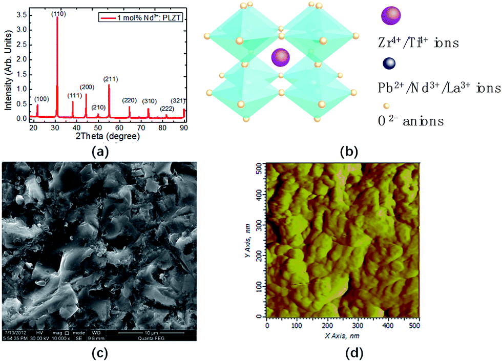
To study the photoinduced scattering and light emission spectrum modulation in typically transparent Nd3+-doped PLZT ceramics, the slugs from which the specimens were cut consisted of 10 mol% lanthanum plus 90 mol% lead in the A-sites and 65 mol% lead zirconate plus 35 mol% lead titanate in the B-sites, which was generally written as PLZT (10/65/35), to which 1.0 mol% Nd3+ ions in the form of Nd2O3 were added. A typical sintering process of the ceramics and the origins of the components used in preparation of the ceramics have been stated elsewhere.33 The solid cylindrically-shaped specimens had a diameter of 2.0 mm and a height of 2.0 mm with a pair of spherical surfaces optically polished and coated with anti-reflection (AR) films. The XRD data of the transparent 1.0 mol% Nd3+-doped PLZT samples was recorded on a X-ray diffractometer (D/MAX-rB, Rigaku, Japan) (Fig. 1(a)). The strong (110) diffraction peaks correspond to a cubic perovskite (ABO3) structure, which consists of A sites occupied with Pb2+ and La3+ ions and a linked network of oxygen octahedral B sites occupied with Zr4+ and Ti4+ ions within the octahedral cage as shown in Fig. 1(b). Since La3+ (added as La2O3) substitutes for Pb2+, the charge balance was maintained by the creation of lattice site vacancies. Similar vacancies can also be formed at the B sites. In addition, as widely accepted, oxygen vacancies can also be formed in a complex oxide like PLZT ceramic. Furthermore, defects could also form on the boundaries of the grains due to the slight variation in the composition among each other. Other disturbed peaks at (111), (200), (210), and (211) were very weak, which implies less pores and impurity mixing at the time of the growth of the specimens. The surface appearance of the prepared 1.0 mol% Nd3+:PLZT specimen was characterized using scanning electron microscopy (SEM) and atomic force microscopy (AFM), as shown in Fig. 1(c) and (d). From these two images, the disordered structure of the specimen from grain to grain could be seen. The intrinsic disordered structure of the Nd3+:PLZT ceramic makes it relatively rich in defects and vacancies, and an ideal material for exploring photoinduced scatterers and multiple scattering of light.
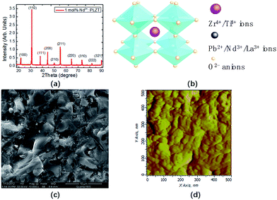 |
| | Fig. 1 (a) X-ray diffraction curve of 1.0 mol% Nd3+-doped PLZT ceramic. (b) Typical ABO3 perovskite structure of PLZT ceramics. Micro-topography of 1.0 mol% Nd3+-doped PLZT ceramics obtained using (c) scanning electron microscope (SEM) and (d) atomic force microscope (AFM). | |
Experimental results and discussion
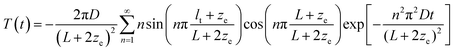
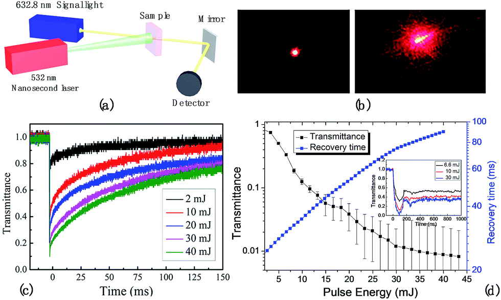
As shown in Fig. 2(a), a continuous wave-signal light centered at 590 nm walked through the 1.0 mol% Nd3+-doped PLZT ceramics. A nanosecond pulse laser centered at 532 nm with pulse width of about 20 nm was used to produce the photoinduced scattering events. After turning on the pulse laser, the intensity of the signal-light spot at the center part decreases rapidly and the scattering patterns around the spot significantly increase, as shown in Fig. 2(b). The dynamic changes of the laser spot intensity were monitored using a Si-based detector and output from an oscilloscope. As shown in Fig. 2(c), the intensity of the signal-light spot at the center part decreased in several nanoseconds along with the laser pulse. Moreover, the stronger the laser pulse energy, the higher was the drop in transmitted light. When the laser pulse energy was 2 mJ, the transmittance of the signal laser spot dropped to 70 percent of its original value, while it decreased to 10 percent when the laser pulse energy reached 40 mJ as shown in the dynamic curve in Fig. 2(c). To avoid missing the lowest point information of the dynamic curves, the decrease in the transmittance of light was recorded in the time scale of 200 ns per grid and the recovery time of transmittance of light was recorded in the time scale of 20 ms per grid. In addition, the intensity of the signal light comes back to its original value gradually within about 30–90 ms, which delayed with the increase in the laser pulse energy as shown in Fig. 2(d). Moreover, the higher the laser pulse energy, the lower was the transmittance, leading to longer recovery time. These experimental results provided direct evidence that photoinduced scattering events occurred when the pulse laser was pumped in the sample.
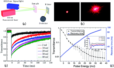 |
| | Fig. 2 (a) Schematic illustration of the photoinduced scattering effect in 1.0 mol% Nd3+-doped PLZT ceramics; (b) signal laser spot changes before and after photoinduced scattering effect; (c) transient changes in the transmittance of light due to the photoinduced scattering effect under different laser energy; (d) changes in the transmittance of light and recovery time vs. laser pulse energy. | |
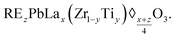
On closing the bandgap energy of the material, free electrons and holes were first excited to the conduction band and recombination centers upon exposure to the laser pulse of 532 nm and trapped by these vacancies and defects in the recombination process (Fig. 3(a)). Afterwards the pumping pulse propagated in the medium was consumed to excite those trapped electrons to the conduction band. These released electrons combined again with the recombination centers, followed by several photons emitting from random frequencies and directions. It appears that the photons are scattered in another direction with a different frequency, which could be defined as the inelastic scattering of light as shown by the colored lines in Fig. 3(b). In addition, the refractive index and optical properties of some local regions could be modified by a large number of trapped electrons or holes accumulation based on the Drude–Lorenz equation in ferroelectric materials, such as lithium niobate (LiNbO3) and (Pb,La)(Zr,Ti)O3 ceramics,34 and III–V semiconductors such as gallium arsenide (GaAs) and indium phosphide (InP) based systems,35 and a refractive index change as large as 0.3 could be estimated. Some of the photons propagated in the medium were scattered directly by the refractive index variation without any energy loss, which is defined as elastic scattering, as shown by the green dashed line in Fig. 3(b). Moreover, a similar photoinduced scattering effect could also be investigated when the specimens were pumped with both ultra-violet light at 405 nm (ref. 36) and infrared light at 808 nm.28 To better understand the photoinduced scattering process, the number of photoinduced scattering events and scattering mean free path length ls were studied both theoretically and experimentally. When the RE3+ ions were doped into the ABO3 perovskite structure, they replace the Pb2+ ions in the A-sites in most cases and the chemical formula of this material could be expressed as follows:
| |
 | (1) |
where ◊ represents the vacancies formed in the A-sites. In addition, when they replace the Zr
4+ and Ti
4+ ions in the B-sites, the chemical formula of this material could be expressed as follows:
| |
 | (2) |
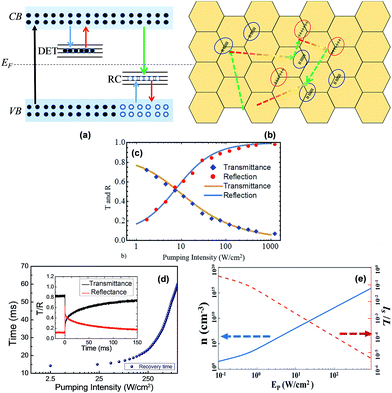 |
| | Fig. 3 (a) Schematic illustration of the band structure and abundant traps distribution in the Nd3+-doped PLZT ceramics. (b) Graphical representation of inelastic and elastic scattering process in the Nd3+-doped PLZT ceramics. (c) Simulation and experimental results for the changes in transmittance and reflection of light along with the pumping intensity (the yellow-brown solid line and blue rhombus points represent the theoretical and experimental results of the transmittance of light, respectively, and the blue-grey solid line and red circular points represent the theoretical and experimental results of the reflections of light, respectively). (d) Recovery time of the original reflectance and transmittance of light (the inset is the dynamic changes in the transmittance and reflectance of light). (e) Concentration of scattering events and scattering mean free path vs. pumping energy at 804 nm. | |
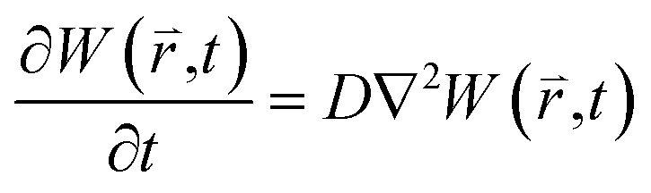
In this study, we made an approximation that all the Nd3+ ions would replace the Pb2+ ions in the A-sites because the number is much higher than that in the B-sites. Based on the eqn (1), the concentration of vacancies in the A-site of 1.0 mol% Nd3+-doped (Pb,La)(Zr,Ti)O3 was calculated as 8.63 × 1020 cm−3. The light propagation dynamic process in disordered medium could be described by the diffusion equation,37
| |
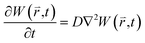 | (3) |
where
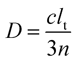
D is the diffusion coefficient, which could be expressed as

, where
c is light velocity in vacuum,
n is the effective refractive index of the specimen, and
lt is the transport mean free path length of light in the scattering medium. Based on the monochromatic transmission matrix,
38 eqn (3) could be derived by the time-reversal method, and the transmittance and reflection of light could be expressed as
39| |
 | (4) |
| |
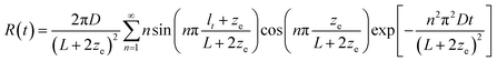 | (5) |
where
L is the optical length of the sample,
ze is the extrapolation length of the incoming light

and
ri is the average internal reflection coefficient, which can be calculated using the Fresnel co-efficient. Then, the total transmittance and reflection of light in disordered media could be written as follows:
| |
 | (6) |
To verify the photoinduced scattering process in the 1.0 mol% Nd3+-doped PLZT ceramics, the transmittance and reflection of light were measured along with an increase in the intensity of the continuous wave diode laser at 804 nm (Apollo Instruments, Inc. S30-804-6). A broad incoherent light source between 400 and 900 nm was collimated and used as a reference beam, which was incident to a slab specimen at 70° to the surface of the sample. The changes in transmittance (T(λ)) and reflectance (R(λ)) of light under an increasing intensity of the diode laser were monitored using a spectrometer, as shown by the blue rhombic and red circular markers in Fig. 3(c). The transmittance curve of light dropped down exponentially along with the increasing reflectance of light, implying that the number of scatterers grew remarkably with the increase in pumping power. In addition, the recovery of the original reflectance and recovery of the original transmittance have the same timescales, as shown in Fig. 3(d); the recovery times increased exponentially along with the increasing reflectance of light. In theory, the number of photoinduced scatterers and transport mean free path length lt in this study could be estimated by the trapped electrons and holes in the specimens. As discussed in our previous study30 and ESI,† the calculation results of the number of the photoinduced scatterers (n) and transport mean free path length (lt) are shown in Fig. 3(e). In addition, based on eqn (2)–(4), the calculation results for the changes in the total transmittance and reflections of light in the 1.0 mol% Nd3+-doped PLZT ceramics could be simulated, as shown by the yellow-brown and blue-grey solid lines in Fig. 3(c), which matched the experimental results very well.
Moreover, the light propagation length in scattering media could not be described only by the thickness of the specimen. This is because the absorption co-efficient of the specimen also changed along with the increased photoinduced scattering events, which could be modified in weak absorption media (αL ≪ 1) as follows:
| |
 | (7) |
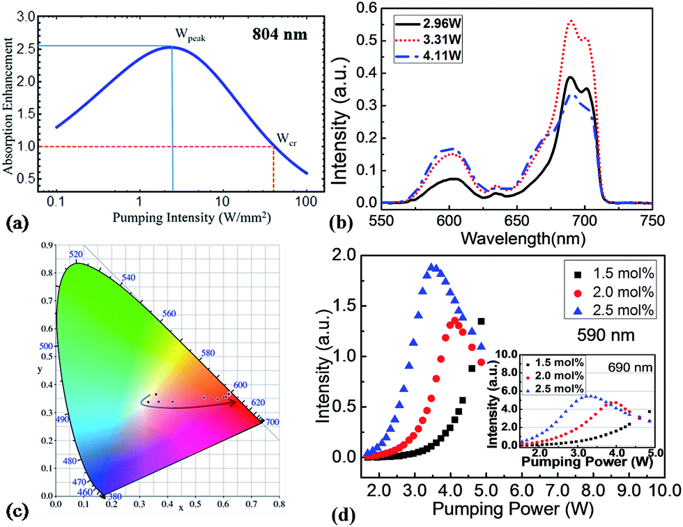
where

is the total propagation length of light in the specimen, which could be much larger than the thickness of the optical direction of the sample. Moreover, the reflection of light (
R) could also increase along with the growing number of scattering events and as a result, the enhancement factor of absorption coefficient of 1.0 mol% Nd
3+-doped PLZT ceramics at 804 nm not only increased but also declined at a critical value, as shown the simulation result in
Fig. 4(a). Hence, there is a threshold beyond which the change in absorption is negative. In this case, the photoluminescence intensity of the sample could also change significantly as shown in
Fig. 4(b). The light emission intensity for all wavelengths increased at first and then decreased gradually upon increasing the pumping power at 804 nm. In this region, the light emission spectra could be controlled effectively because the ratio of the two major emission peaks are very sensitive to the scattering intensity. As shown in
Fig. 3(c), the chromatograph of light emission under different pumping powers was recorded using CIE1931 Chromaticity Coordinate Calculation software; the color of the light emission changed greatly from dark white to luminous yellow, then to red and finally to yellow-red around 600 nm. To further study the influence of the photoinduced scattering effect on light emission and absorption modification in the Nd
3+-doped PLZT ceramics, the light emission intensity of the 1.5, 2.0 and 2.5 mol% Nd
3+-doped PLZT ceramics was measured under different pumping intensities at 590 nm and 690 nm as shown in
Fig. 4(d). With higher Nd
3+ ions-doping in the samples, more vacancies were formed in the replacement process, followed by more electrons and holes trapped in the specimen. As a result, the photoinduced scattering effect was enhanced and the absorption and light emission peaks occurred at a lower pumping intensity.
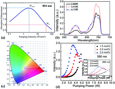 |
| | Fig. 4 (a) Enhancement of absorption coefficient under different pumping intensities. (b) Light emission spectra at different pumping powers. (c) Chromatograph of light emission changes recorded using CIE1931 Chromaticity Coordinate Calculation software. (d) Light emission intensity of 1.5, 2.0 and 2.5 mol% Nd3+-doped PLZT ceramics vs. pumping power at 590 nm and 690 nm. | |
These experimental and theoretical simulation results could be applied in many aspects. First, the photoinduced refractive index change could be increased to 0.3 and such strong scattering events could be designed intentionally to study random lasers and the weak localization of light. Second, the light emission intensity could be modified by the scattering intensity of the sample, which is promising for the design of highly efficient photoelectric devices, solar cells and lasers. Third, they provide another strategy to tune the chromatograph of light emission for white light generation.
Conclusions
In conclusion, the photoinduced scattering effect formed by both pulse laser and continuous wave laser has been investigated in Nd3+-doped lead lanthanum zirconate titanate (PLZT) ceramics. The changes in the transmittance, reflectance and absorption coefficients of light along with the scattering strength were studied theoretically and experimentally, which matched well with each other. The increased absorption and reflection of light observed for the 1.5, 2.0 and 2.5 mol% Nd3+-doped PLZT ceramics were used to modulate the light emission intensity and optimized light emission intensities were obtained at different scattering strengths. This study is extremely promising for the design of photoinduced scattering structures, exploring random lasers and Anderson localization of light, designing highly efficient photoelectric devices and solar cells, and tuning the chromatograph of light emission for white light generation.
Conflicts of interest
There are no conflicts to declare.
Acknowledgements
This study is supported by the grant of Fundamental Research Funds for the Central Universities of China under project XDJK2017C061 and SWU116051 and National Natural Science Foundation of China under project No. 11374076.
References
- D. S. Wiersma and A. Lagendijk, Phys. Rev. E: Stat. Phys., Plasmas, Fluids, Relat. Interdiscip. Top., 1996, 54(4), 4256 CrossRef CAS.
- M. Law, L. E. Greene, J. C. Johnson, R. Saykally and P. Yang, Nat. Mater., 2005, 4(6), 455 CrossRef CAS PubMed.
- R. Horstmeyer, H. Ruan and C. Yang, Nat. Photonics, 2015, 9(9), 563–571 CrossRef CAS PubMed.
- P. W. Anderson, Phys. Rev., 1958, 109(5), 1492–1505 CrossRef CAS.
- H. Cao, Y. G. Zhao, S. T. Ho, E. W. Seelig, Q. H. Wang and R. P. H. Chang, Phys. Rev. Lett., 1999, 82(11), 2278 CrossRef CAS.
- D. S. Wiersma, Nat. Photonics, 2013, 7(3), 188–196 CrossRef CAS.
- X. Y. Liu, C. X. Shan, S. P. Wang, Z. Z. Zhang and D. Z. Shen, Nanoscale, 2012, 4(9), 2843–2846 RSC.
- Q. Song, S. Xiao, Z. Xu, J. Liu, X. Sun, V. Drachev and Y. L. Kim, Opt. Lett., 2010, 35(9), 1425–1427 CrossRef PubMed.
- D. S. Wiersma, Nat. Phys., 2008, 4(5), 359–367 CrossRef CAS.
- S. F. Yu, C. Yuen, S. P. Lau and H. W. Lee, Appl. Phys. Lett., 2004, 84(17), 3244–3246 CrossRef CAS.
- N. Bachelard, S. Gigan, X. Noblin and P. Sebbah, Nat. Phys., 2014, 10(6), 426–431 CrossRef CAS.
- J. H. Noh, S. H. Im, J. H. Heo, T. N. Mandal and S. I. Seok, Nano Lett., 2013, 13(4), 1764–1769 CrossRef CAS PubMed.
- V. E. Ferry, L. A. Sweatlock, D. Pacifici and H. A. Atwater, Nano Lett., 2008, 8(12), 4391–4397 CrossRef CAS PubMed.
- Q. Zhang and G. Cao, Nano Today, 2011, 6(1), 91–109 CrossRef CAS.
- J. A. Chang, J. H. Rhee, S. H. Im, Y. H. Lee, H. J. Kim, S. I. Seok and M. Gratzel, Nano Lett., 2010, 10(7), 2609–2612 CrossRef CAS PubMed.
- F. Fabregat-Santiago, G. Garcia-Belmonte, I. Mora-Seró and J. Bisquert, Phys. Chem. Chem. Phys., 2011, 13(20), 9083–9118 RSC.
- A. J. Frank, N. Kopidakis and J. van de Lagemaat, Coord. Chem. Rev., 2004, 248(13), 1165–1179 CrossRef CAS.
- A. S. Gomes, E. P. Raposo, A. L. Moura, S. I. Fewo, P. I. Pincheira, V. Jerez and C. B. De Araújo, Sci. Rep., 2016, 6, 27987 CrossRef CAS PubMed.
- F. Luan, B. Gu, A. S. Gomes, K. T. Yong, S. Wen and P. N. Prasad, Nano Today, 2015, 10(2), 168–192 CrossRef CAS.
- A. L. Moura, V. Jerez, L. J. Maia, A. S. Gomes and C. B. De Araújo, Sci. Rep., 2015, 5, 13816 CrossRef PubMed.
- M. R. Leyden, L. K. Ono, S. R. Raga, Y. Kato, S. Wang and Y. Qi, J. Mater. Chem. A, 2014, 2(44), 18742–18745 CAS.
- S. Sivasubramaniam and M. M. Alkaisi, Microelectron. Eng., 2014, 119, 146–150 CrossRef CAS.
- A. Aho, V. Polojärvi, V. M. Korpijärvi, J. Salmi, A. Tukiainen, P. Laukkanen and M. Guina, Sol. Energy Mater. Sol. Cells, 2014, 124, 150–158 CrossRef CAS.
- Z. Su, K. Sun, Z. Han, H. Cui, F. Liu, Y. Lai and M. A. Green, J. Mater. Chem. A, 2014, 2(2), 500–509 CAS.
- X. Zhang, H. Liu, X. Huang and H. Jiang, J. Mater. Chem. C, 2015, 3(14), 3336–3341 RSC.
- A. Büchler, S. Kluska, F. Meyer, A. A. Brand, G. Cimiotti, J. Bartsch and M. Glatthaar, Sol. Energy Mater. Sol. Cells, 2017, 166, 197–203 CrossRef.
- J. Zhang, L. Xu, L. Wang, F. Huang, X. Sun, H. Zhao and X. Chen, Appl. Phys. Lett., 2013, 102(2), 021109 CrossRef.
- L. Xu, J. Zhang, C. Xu and H. Zhao, J. Lumin., 2016, 173, 185–191 CrossRef CAS.
- L. Xu, H. Zhao, C. Xu, S. Zhang, Y. K. Zou and J. Zhang, Appl. Opt., 2014, 53(4), 764–768 CrossRef CAS PubMed.
- C. Xu, J. Zhang, L. Xu and H. Zhao, Opt. Mater. Express, 2017, 7(6), 1745–1753 CrossRef.
- L. Xu, H. Zhao, S. Zhang, C. Xu, Y. K. Zou and J. Zhang, J. Appl. Phys., 2013, 113(22), 223101 CrossRef.
- L. Xu, H. Zhao, S. Zhang, C. Xu and J. Zhang, J. Appl. Phys., 2014, 116(6), 063104 CrossRef.
- G. H. Haertling, Ferroelectrics, 1987, 75(1), 25–55 CrossRef CAS.
- E. Feigenbaum, K. Diest and H. A. Atwater, Nano Lett., 2010, 10(6), 2111–2116 CrossRef CAS PubMed.
- C. Xu, J. Zhang, L. Xu, X. Ma and H. Zhao, J. Appl. Phys., 2017, 121(24), 243104 CrossRef CAS; G. T. Reed and C. E. Png Jason, Mater. Today, 2005, 8(1), 40–50 CrossRef.
- C. Xu, J. Zhang, L. Xu and H. Zhao, J. Appl. Phys., 2015, 117(2), 023107 CrossRef.
- D. S. Wiersma, A. Muzzi, M. Colocci and R. Righini, Phys. Rev. E: Stat. Phys., Plasmas, Fluids, Relat. Interdiscip. Top., 2000, 62(5), 6681 CrossRef CAS.
- S. M. Popoff, G. Lerosey, R. Carminati, M. Fink, A. C. Boccara and S. Gigan, Phys. Rev. Lett., 2010, 104(10), 100601 CrossRef CAS PubMed.
- R. Mupparapu, K. Vynck, T. Svensson, M. Burresi and D. S. Wiersma, Opt. Express, 2015, 23(24), A1472–A1484 CrossRef PubMed.
Footnote |
| † Electronic supplementary information (ESI) available. See DOI: 10.1039/c7ra07597a |
|
| This journal is © The Royal Society of Chemistry 2017 |
Click here to see how this site uses Cookies. View our privacy policy here. 
 Open Access Article
 This Open Access Article is licensed under a
  *ab,
Jingwen Zhangb,
Hua Zhaob and
Caixia Xu*c
*ab,
Jingwen Zhangb,
Hua Zhaob and
Caixia Xu*c

 , where c is light velocity in vacuum, n is the effective refractive index of the specimen, and lt is the transport mean free path length of light in the scattering medium. Based on the monochromatic transmission matrix,38 eqn (3) could be derived by the time-reversal method, and the transmittance and reflection of light could be expressed as39

 and ri is the average internal reflection coefficient, which can be calculated using the Fresnel co-efficient. Then, the total transmittance and reflection of light in disordered media could be written as follows:

 is the total propagation length of light in the specimen, which could be much larger than the thickness of the optical direction of the sample. Moreover, the reflection of light (R) could also increase along with the growing number of scattering events and as a result, the enhancement factor of absorption coefficient of 1.0 mol% Nd3+-doped PLZT ceramics at 804 nm not only increased but also declined at a critical value, as shown the simulation result in Fig. 4(a). Hence, there is a threshold beyond which the change in absorption is negative. In this case, the photoluminescence intensity of the sample could also change significantly as shown in Fig. 4(b). The light emission intensity for all wavelengths increased at first and then decreased gradually upon increasing the pumping power at 804 nm. In this region, the light emission spectra could be controlled effectively because the ratio of the two major emission peaks are very sensitive to the scattering intensity. As shown in Fig. 3(c), the chromatograph of light emission under different pumping powers was recorded using CIE1931 Chromaticity Coordinate Calculation software; the color of the light emission changed greatly from dark white to luminous yellow, then to red and finally to yellow-red around 600 nm. To further study the influence of the photoinduced scattering effect on light emission and absorption modification in the Nd3+-doped PLZT ceramics, the light emission intensity of the 1.5, 2.0 and 2.5 mol% Nd3+-doped PLZT ceramics was measured under different pumping intensities at 590 nm and 690 nm as shown in Fig. 4(d). With higher Nd3+ ions-doping in the samples, more vacancies were formed in the replacement process, followed by more electrons and holes trapped in the specimen. As a result, the photoinduced scattering effect was enhanced and the absorption and light emission peaks occurred at a lower pumping intensity.