
 Open Access Article
 This Open Access Article is licensed under a
 Creative Commons Attribution 3.0 Unported Licence
Nonlinear optical properties of metal nanoparticles: a review
Yu-xi Zhang and
Yu-hua Wang *
*
Hubei Province Key Laboratory of Science in Metallurgical Process, Wuhan University of Science and Technology, Wuhan 430081, China. E-mail: wangyuhua@wust.edu.cn; Fax: +86-27-68862772; Tel: +86-27-61094568
First published on 21st September 2017
Abstract
Metal nanoparticles (MNPs) hold great technological promise because of the possibility of engineering their electronic and optical properties through material design. One of the effective methods to fabricate MNPs is ion implantation. In this review, recent results on the nonlinear optical properties of nanoparticles (including copper, silver, gold, and bismuth nanoparticles) doped in various bases have been discussed. Some specific optical nonlinear properties, such as nonlinear refraction, two-photon absorption, and optical limiting, for femtosecond, picosecond, and nanosecond laser pulses have also been covered. In addition to ion implantation, we have summarized several other methods for the preparation of composite materials, and Z-scan has been used to study the nonlinear optical properties of these materials.
1 Nonlinear optical properties
1.1 Introduction
Some important formulas describing ordinary optical phenomena often exhibit mathematical linear characteristics. For example, to explain the refractive index, scattering, and birefringence of the medium, an important physical mass-dielectric polarization vector P was introduced, and it was speculated that it had a simple linear relationship with the incident wave field E, that is
| P = χE | (1) |
To make a perfect interpretation of the effects of optical secondary harmonics, third harmonic and rectification effects were observed in a series of media. In this regard, it is necessary to speculate that under the action of an intense laser, the dielectric strength of the medium is no longer linearly related to the intensity of the incident light field, but rather a more general power relationship (including the nonlinear component, which is proportional to the high power of the field) must be applied. That is
| P = χ(1)E + χ(2)EE + χ(3)EEE +… | (2) |
In the last two decades, a variety of studies have been performed on the NOPs of novel materials because of the potential of these materials in optical device applications,10 and novel materials with enhanced nonlinearities need to be identified.11 It was thought that many nonlinear effects could only be observed on the bulk scale, but researchers showed that some nonlinear effects could occur at the nano-scale. As is known, nonlinear optical nanomaterials have a potential to enhance the efficiency and extend the applications of this technique in many new device applications such as in the areas of communications,12 optical devices,13 biosensors, and imaging. Nanomaterials with large nonlinear responses can be used as contrast agents in nonlinear microscopy,14 photocatalysis, and optical limiting applications.15
In the past two decades, efficient nonlinear optical materials have made significant progress in laser technology, and these materials have large nonlinear optical properties and a fast nonlinear response for various photonic and optoelectronic applications such as laser ablation, pulsed laser deposition, optical communication, optical information processing, and optical data storage and as optical limiters.16–21 Optical limiting is one of the most promising practical applications of all nonlinear optical properties and can be used to protect the human eye and photosensitive components of delicate optical instruments from damage caused by intense optical radiation.22 Optical limiters strongly attenuate a potentially dangerous laser beam while exhibiting a transmittance to low ambient light.23 Some of the materials used for nonlinear optical limiting applications are GaSe, CdSe, AgAsS3, and LiIO3, which have utility for different applications.24 In addition, electro-optic crystals, such as LiNbO3, BaTiO3, and KNbO3, have major potential for nonlinear optical limiting applications.25
The search for new nanostructured materials is one of the defining characteristics of modern science and technology.26 New nanostructured materials can be used to fabricate many devices such as new mechanical, electrical, magnetic, chemical, biological, and optical devices. This review summarizes the advances, such as the development of nonlinear optical random metal–dielectric and metal–semiconductor composites based on metal nanoparticles (MNPs) synthesized by ion implantation,28 made in optical science and technology in recent years.27 While seeking and developing new technologies for the synthesis of nanoparticles, substantial practical efforts are made to control the size of the MNP. This is because different applications require different optical properties, and the optical properties are determined by the size of the MNP. In this context, ion implantation nanotechnology allows the fabrication of materials with almost any MNP structures, types of metals, and their alloys29 and opens up a new way for the fabrication of nanomaterials with the required properties. The electromagnetic properties of these composites are very special, and these composites are very different from the ordinary bulk materials because they may become even more important in the drive towards the miniaturization of electronic and optoelectronic components.
Nonlinear optics plays a key role in the realization and development of many photon technologies, and it can be used to process the optical signal information at enhanced speed. Novel nonlinear optical materials with an ultrafast response time, high resistance to bulk and surface laser damage, and low two-photon absorption have been fabricated, and large optical nonlinearities are critical for their implementation in many applications. Nonlinear materials with these characteristics are also widely used in waveguide applications.
With the development of waveguide media with intensity-dependent refractive indices, optoelectronic devices can be converted into all-optical configurations. A huge enhancement of the nonlinear optical response in random media with MNPs is often associated with optical excitation of the surface plasmon resonances (SPR) that are collective electromagnetic modes and strongly dependent on the geometry structure of the composite medium.30 Therefore, MNP-containing transparent dielectric and semiconductor materials can be effectively used in new integrated optoelectronic devices.
Although both the classical and quantum-mechanical effects in the linear optical response of MNP composites have been studied for decades, the first experimental results on the nonlinear optical effects in MNPs in ruby-glass have been obtained quite recently by Ricard et al. in 1985.31 The ability to create nonlinear optical elements with MNPs for application in all-optical switching and computing devices has generated significant interest, and consequently, various studies have been directed at the preparation of composite materials. In practice, to make a composite material in the SPR spectral region, a strong linear absorption is required; thus, attempts are being made to improve the concentration of the MNPs. When all the other parameters of the composite are the same, a system with a higher fill factor will have a higher nonlinear susceptibility.
1.2 Z-Scan technique
In 1989, Sheik-Bahae et al.32 proposed a new method for measuring the nonlinear refractive index of nonlinear optical materials. The method was characterized by high sensitivity and single-beam measurement. Since the test sample is required to move along the direction of the optical axis, the method is referred to as the Z-scan method. In 1990, Sheik-Bahae et al.33 applied this method to the nonlinear absorption coefficient of a measurement material. In 1992, Sheik-Bahae et al. proposed a two-color Z-scan method and applied it to measure non-degenerate nonlinear and non-degenerate nonlinear two-photon absorption coefficients. Within a short time period, the Z-scan technology has continuously improved, and it has been tested and studied in other aspects such as thermal lens effects, laser beam quality testing, and Gaussian beam transmission characteristics. Z-Scanning technology has since developed into having a significant practical value among the test methods used in the study of nonlinear optical properties.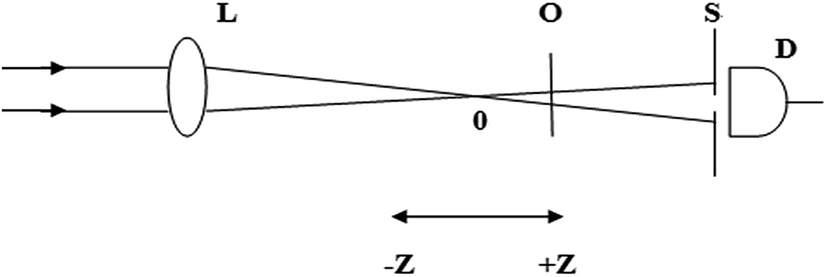 | ||
| Fig. 1 Schematic of the basic device of the Z-scan method. | ||
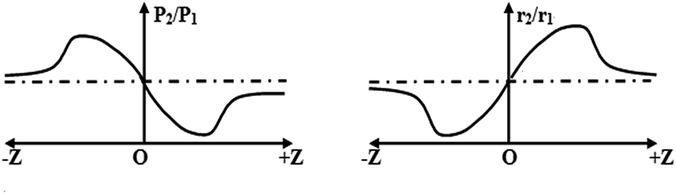 | ||
| Fig. 2 Z-Scan curve for (left) negative optical nonlinear samples and (right) positive optical nonlinear samples. | ||
| Pi(t) = πω02I0(t)/2 | (3) |
| s = 1 − exp(−2ra2/ωa2) | (4) |
 | (5) |
The phase change of the wave surface at the focal point on the axis is
| Δφ0 = kΔn0(t)Leff | (6) |
Among them,  , λ is the laser wavelength, Leff = (1 − e−αL), α is the linear absorption coefficient, L is the sample thickness, and Δn0 = γI0(t).
By definition ΔTP-V = TP − T, which represents the difference in the normalized transmittance of the peak-valley in the normalized Z-scan curve, when Δφ0 ≤ π
| ΔTP-V ≈ 0.406(1 − s0.25)|Δφ0| | (7) |
Therefore, according to the obtained Z-scan curve, γ can be obtained using (6) and (7).
| α(I) = α + βI | (8) |
 | (9) |
| q0(z,t) = βI0(t)Leff/(1 + z2/z02), when |q0| < 1, |
 | (10) |
When a Z-scan is performed without an aperture, numerical fitting can be conducted on the experimental results according to the abovementioned formula.
2 NOPs of metal ions implanted into various matrices
In many studies, composite materials with MNPs exhibiting nonlinear optical characteristics were fabricated by various methods and then generally studied using lasers operating at frequencies corresponding to the spectral range of the SPR, as shown in Table 1. However, in fact, when novel materials with MNPs are used, their properties should be systematically studied. Hence, to create new materials promising for practical use in laser systems and integral optics and to optimize their characteristics, the nonlinear optical properties of these materials should be studied not only in the SPR spectral region but also at the specific lasers for industry need.| Metal (ion) | Matrix | Synthesis conditions: energy (E), keV, dose (D), ion per cm2, current density (J), μA cm−2, annealing temperature (T), °C, time (t) ps | Study nonlinear optical method | Laser parameters: wavelength (λ), nm, pulse duration (τ), ps, repetition rate (ν), Hz, intensity (I0), W cm−2, pulse energy (P) mJ | Nonlinear parameters: refract. coeff. (n2), cm2 W−1, absorption coeff. (β), cm W−1, satur. intensity (Isat), W cm−2, Re[χ(3)], Im[χ(3)], [χ(3)], esu | Author |
|---|---|---|---|---|---|---|
| Cu | STO (SrTiO3) | D = 1 × 10¹⁶, t < 1 | DFWM, Z-scan | λ = 775 nm, τ = 250 fs, ν = 1000 Hz | β = 1.78 × 10⁻¹², χ(3) = 1.55 × 10⁻¹⁰, [χ(3)] = 2.2 × 10⁻¹⁰ | Cetin et al. 2010 (ref. 35) |
| Cu | STO (SrTiO3) | D = 5 × 10¹⁶, t = 2.46 | DFWM, Z-scan | λ = 775 nm, τ = 250 fs, ν = 1000 Hz | β = 4.23 × 10⁻¹², χ(3) = 3.66 × 10⁻¹⁰, [χ(3)] = 4.5 × 10⁻¹⁰ | |
| Tb | STO (SrTiO3) | D = 1 × 10¹⁷, t = 3.58 | DFWM, Z-scan | λ = 775 nm, τ = 280 fs, ν = 1000 Hz | β = 6.15 × 10⁻¹², χ(3) = 5.33 × 10⁻¹⁰, [χ(3)] = 6.54 × 10⁻¹⁰ | |
| Tb | STO (SrTiO3) | D = 1 × 10¹⁷, t = 3.58 | DFWM, Z-scan | λ = 775 nm, τ = 280 fs, ν = 1000 Hz | β = 5.53 × 10⁻¹², χ(3) = 4.79 × 10⁻¹⁰, [χ(3)] = 5.9 × 10⁻¹⁰ | |
| Tb | STO (SrTiO3) | D = 5 × 10¹⁶, t = 3.55 | DFWM, Z-scan | λ = 775 nm, τ = 280 fs, ν = 1000 Hz | β = 11.6 × 10⁻¹², χ(3) = 10 × 10−10, [χ(3)] = 12.5 × 10⁻¹⁰ | |
| Tb | STO (SrTiO3) | D = 1 × 10¹⁷, t = 4.15 | DFWM, Z-scan | λ = 775 nm, τ = 280 fs, ν = 1000 Hz | β = 13.4 × 10⁻¹², χ(3) = 11.6 × 10⁻¹⁰, [χ(3)] = 14.2 × 10⁻¹⁰ | |
| As2+ | GaAs–AlGaAs | E = 4 × 10³, D = 5 × 10¹², T = 775, t > 60 | λ = 1545–1565, ν = 7.56 × 10⁷ | n2 = 71% | Wagner et al. 2009 (ref. 36) | |
| Ag | SiNx | E = 4 × 10³, D = 1.5 × 10¹⁶, D = 3.0 × 10¹⁶, D = 4.5 × 10¹⁶ | HRTEM, XS-TEM | λ = 475 nm | Bayle et al. 2015 (ref. 37) | |
| Ag | SiO2 | E = 200, D = 2 × 10¹⁷ | Z-Scan | λ = 532 nm | χ(3) = 4.0 × 10⁻⁸ | Wang et al. 2008 (ref. 38) |
| Ag | SiO2 | E = 200, D = 2 × 10¹⁷ | Z-Scan | λ = 1064 nm | χ(3) = 9.0 × 10⁻⁸ | |
| Ag | SiO2 | E = 130, J = 2, D = 3 × 10¹⁶, T = 800, t = 60 | TEM, Z-scan | λ = 300–800 nm | β = (−3.42 ± 0.06) × 10−4, Is = (1.02 ± 0.03) × 107 | Cesca et al. 2010 (ref. 39) |
| Ag | SiO2 | E = 130, J = 2, D = 3 × 10¹⁶, E = 190, J = 0.2, D = 2.5 × 10¹⁶ (Ar) | TEM, Z-scan | λ = 300–800 nm | β = (−3.0 ± 0.4) × 10−4, Is = (1.21 ± 0.05) × 109 | |
| Ag | 72GeS2–18Ga2S3–10CdS | E = 70, D = 1 × 10¹⁶ | Z-Scan, AFM | λ = 700 nm | χ(3) = 1.58 × 10⁻¹¹ | Song et al. 2015 (ref. 40) |
| Ag | 72GeS2–18Ga2S3–10CdS | E = 70, D = 3 × 10¹⁶ | Z-Scan, AFM | λ = 700 nm | χ(3) = 4.83 × 10⁻¹¹ | |
| Ag | 72GeS2–18Ga2S3–10CdS | E = 70, D = 3 × 10¹⁶ | Z-Scan, AFM | λ = 700 nm | χ(3) = 5.70 × 10⁻¹¹ | |
| Ag | 72GeS2–18Ga2S3–10CdS | E = 70, D = 1 × 10¹⁷ | Z-Scan, AFM | λ = 700 nm | χ(3) = 7.58 × 10⁻¹¹ | |
| Ag | 72GeS2–18Ga2S3–10CdS | E = 70, D = 2 × 10¹⁷ | Z-Scan, AFM | λ = 700 nm | χ(3) = 2.87 × 10⁻¹¹ | |
| Au | SiO2 | E = 190, J = 2, D = 3 × 10¹⁶, T = 800, t = 60 (air) | TEM, Z-scan | λ = 300–800 nm | β = (1.7 ± 0.2) × 10−4, Is = (3.2 ± 0.5) × 108 | Sánchezdena et al. 2013 (ref. 41) |
| Au | SiO2 | E = 190, J = 2, D = 3 × 10¹⁶, J = 0.2, D = 2.5 × 10¹⁶ (Ar) | TEM, Z-scan | λ = 300–800 nm | β = (16 ± 8) × 10−4, Is = (1.0 ± 0.4) × 107 | |
| Au | αAI2O3 | E = 1.5–2.0 × 10³, D = 2.5–8 × 10¹⁶ | Z-Scan | λ = 532 nm | β = −4 × 10⁻¹², I0 = 3.1 × 10¹⁴, n2 = 3.1 × 10⁻¹⁵ | |
| Au | αAI2O3 | E = 1.5–2.0 × 10³, D = 2.5–8 × 10¹⁶ | Z-Scan | λ = 355 nm | β = 1.5 × 10⁻¹², I0 = 3.36 × 10¹⁴ | |
| Au | Al2O3 | DFWM, Z-scan | λ = 525 nm, τ = 5.2 ns, ν = 10 Hz, I0 = 5.7 × 10⁶ | β = −1.31 × 10⁻³, χ(3) = 1.58 × 10⁻⁷, [χ(3)] = 6.25 × 10⁻⁸, Im[χ(3)] = −5.33 × 10⁻⁷, Re[χ(3)] = 5.03 × 10⁻⁷, n2 = 7.62 × 10⁻⁹ | Ryasnyanskiy et al. 2007 (ref. 42) | |
| Au | SiO2 | DFWM, Z-scan | λ = 540 nm, ν = 5.8 ns, I0 = 28 × 106 | β = −0.12 × 10⁻³, χ(3) = 1.38 × 10⁻⁷, [χ(3)] = 2.7 × 10⁻⁸, Im[χ(3)] = −0.067 × 10⁻⁷, Re[χ = 2.97 × 10⁻⁹ | ||
| Au | ZnO | DFWM, Z-scan | λ = 500 nm, ν = 5.9 ns, I0 = 8 × 10⁶ | β = −0.08 × 10⁻³, χ(3) = 1.47 × 10⁻⁷, [χ(3)] = 2.46 × 10⁻⁸, Im[χ(3)] = −0.044 × 10⁻⁷, Re[χ(3)] = −1.47 × 10⁻⁷, n2 = −1.31 × 10⁻⁹ | ||
| Au | BTEAADT (2-thioxo-1,3-dithiole-4,5-dithiolato) | Z-Scan | λ = 532 nm | β = 2.839 × 10⁻⁹, χ(3) = 9.410 × 10⁻¹³, n2 = −1.685 × 10⁻¹⁴, γ = 6.770 × 10⁻³¹, (γ: hyperpolarizability) | Chen et al. 2012 (ref. 43) | |
| BTEAADT | Z-Scan | λ = 1064 nm | χ(3) = 6.638 × 10⁻¹³, n2 = −1.459 × 10⁻¹⁴, γ = 4.303 × 10⁻³¹ | |||
| Au-NPs | SiO2 | E = 2 × 10³, D = 5 × 10¹⁶ | Z-Scan | λ = 825 nm, t = 80 fs | β = −1.51 × 10⁻⁷, [χ(3)] = 1.21 × 10⁻¹⁰, n2 = 8.94 × 10⁻¹¹ | Torres-Torres et al. 2015 (ref. 44) |
| Au-NPs | SiO2 | E = 2 × 10³, D = 5 × 10¹⁶ | Z-Scan | λ = 532 nm, t = 1 ns | [χ(3)] = 2.2 × 10⁻⁹ | |
| Si-QDs & Au-NP | SiO2 | E1 = 1.5 × 10³, D1 = 2.5 × 10¹⁷, E2 = 1.5 × 10³, D2 = 8.5 × 10¹⁶ | Z-Scan | λ = 825 nm, t = 80 fs | β = −1.26 × 10⁻⁶, [χ(3)] = 2.6539 × 10⁻⁹, n2 = 3.37 × 10⁻¹¹ | |
| Si-QDs &Au-NP | SiO2 | E = 1.5 × 10³, D = 2.5 × 10¹⁷, E2 = 1.5 × 10³, D2 = 8.5 × 10¹⁶ | Z-Scan | λ = 532 nm, t = 1 ns | [χ(3)] = 3.5 × 10⁻⁹ | Torres-Torres et al. 2015 (ref. 44) |
| Si-QDs | SiO2 | E = 1.5 × 10³, D = 2.5 × 10¹⁷, T = 1100 °C, T = 90 min, (50% H2 + 50% N2) | Z-Scan | λ = 825 nm, t = 80 fs | β = −1.51 × 10⁻⁵, [χ(3)] = 8.682 × 10⁻⁹, n2 = 5.55 × 10⁻¹¹ | |
| Si-QDs | SiO2 | E = 1.5 × 10³, D = 2.5 × 10¹⁷, T = 1100 °C, t = 90 min, (50% H2 + 50% N2) | Z-Scan | λ = 532 nm, t = 1 ns | [χ(3)] = 5.3 × 10⁻¹⁰ | Torres-Torres et al. 2015 (ref. 44) |
| Mg | ZnO | E = 3.24 × 10⁻³ | XPS, Z-scan, UV-Vis | λ = 490 nm | β = 58 × 10−6, Im[χ(3)] = 5.91 × 10⁻¹¹, Re[χ(3)] = 2.78 × 10⁻¹¹, n2 = −2.04 × 10⁻⁵ | Agrawal et al. 2015 (ref. 45) |
| Mg | Mg0.09Zn0.91Q | E = 3.37 × 10⁻³ | XPS, Z-scan, UV-Vis | λ = 550 nm | β = 448 × 10−6, Im[χ(3)] = 41.99 × 10⁻¹¹, Re[χ(3)] = 3.08 × 10⁻¹¹, n2 = −2.46 × 10⁻⁵ | |
| Mg | Mg0.21Zn0.79Q | E = 3.49 × 10⁻³ | XPS, Z-scan, UV-Vis | λ = 590 nm | β = 455 × 10−6, Im[χ(3)] = 36.41 × 10⁻¹¹, Re[χ(3)] = 2.50 × 10⁻¹¹, n2 = −2.36 × 10⁻⁵ | |
| Ni | BTEANDT (2-thioxo-1,3-dithiole-4,5-dithiolato) | Z-Scan | λ = 532 nm | χ(3) = 7.84 × 10⁻¹³, n2 = −1.452 × 10⁻¹⁴, γ = 6.770 × 10⁻³¹, (γ: hyperpolarizability) | Chen et al. 2012 (ref. 43) |
Nowadays, high-speed optical devices require materials with high values of nonlinear optical parameters such as nonlinear refractive index and nonlinear absorption coefficient.46 For Cu, with the increasing dose number, the absorption coefficient and the χ(3) also increases under the same detection conditions, but the synthesis conditions are different. The results of new investigations on the nonlinear optical parameters of composite materials based on an STO matrix with Cu and Tb nanoparticles are presented. They showed that the effective third-order nonlinear susceptibility is real and has a positive sign. DFWM and Z-scan measurements showed that the value of |χ(3)| increased with an increase in the implantation dose. Moreover, the slow component of the relaxation time increased (from 0.1 to 3.58 units for Cu and from 2.52 to 4.15 for Tb nanoparticles).
Ag was implanted into the matrix of SiO2, and the sample was tested at the wavelengths 532 nm and 1064 nm; the sample tested at the lower wavelength had a lower χ(3); this indicated that this new structure of metal nanoclusters represented a new aspect for the study of the nonlinear optical response. However, if the synthesis conditions were changed, the nonlinear parameters changed together. Furthermore, experiments showed that the nonlinear absorption properties of the samples were affected after Ar irradiation. The results revealed the large nonlinear absorption properties of these systems, as characterized by the concomitance of saturable and reverse saturable absorption.
The third-order nonlinearity of 72GeS2–18Ga2S3–10CdS chalcogenide glass implanted by Ag ions was studied. The doses for implantation ranged from 1 × 10¹⁶ to 2 × 10¹⁷ ions per cm2, and the Ag nanoparticles were observed via AFM measurements. The third-order nonlinear optical property χ(3) was measured by the femtosecond Z-scan technique and showed a maximum value of 7.58 × 10⁻¹¹ esu.
This indicated that the χ(3) enhancement of the implanted samples was due to the formation of Ag nanoparticles. The relation between the implanted dose and the third-order nonlinearity was associated with the enhancement of the local field inside the particles and the interaction between Ag nanoparticles, which could be useful in the fabrication of optical devices by controlling the implanted doses to control the optical nonlinearity in glasses.
2.1 Nonlinear optical studies of Au
The third-order NOPs of gold nanoparticles implanted into various matrices (Al2O3, ZnO, and SiO2) have been investigated by the Z-scan method. The nonlinear refractive index, nonlinear absorption coefficient, and the real and imaginary parts of the third-order nonlinear susceptibility have been deduced.41 According to the results, when the wavelength was between 300 nm and 800 nm, it was clear that the annealing atmosphere could affect the absorption coefficient. The samples annealed in air had a lower absorption coefficient than the sample annealed in Ar. Regarding the nonlinear optical response, it was found that the isotropic sample exhibited negative and positive nonlinear absorption at the wavelengths of 532 nm and 355 nm, respectively (Fig. 3). The nonlinear coefficients were β = −4 × 10⁻¹² m W−1 with an irradiance value of I0 = 3.1 × 10¹⁴ W m−2 for 532 nm, and β = 1.5 × 10⁻⁸ m W−1 with I0 = 3.36 × 10¹⁴ W m−2 for 355 nm. Moreover, the nonlinear refraction was found to be positive for 532 nm with a value of n2 = 3.1 × 10⁻¹⁵ m2 W−1, but it vanished at 355 nm (Fig. 4).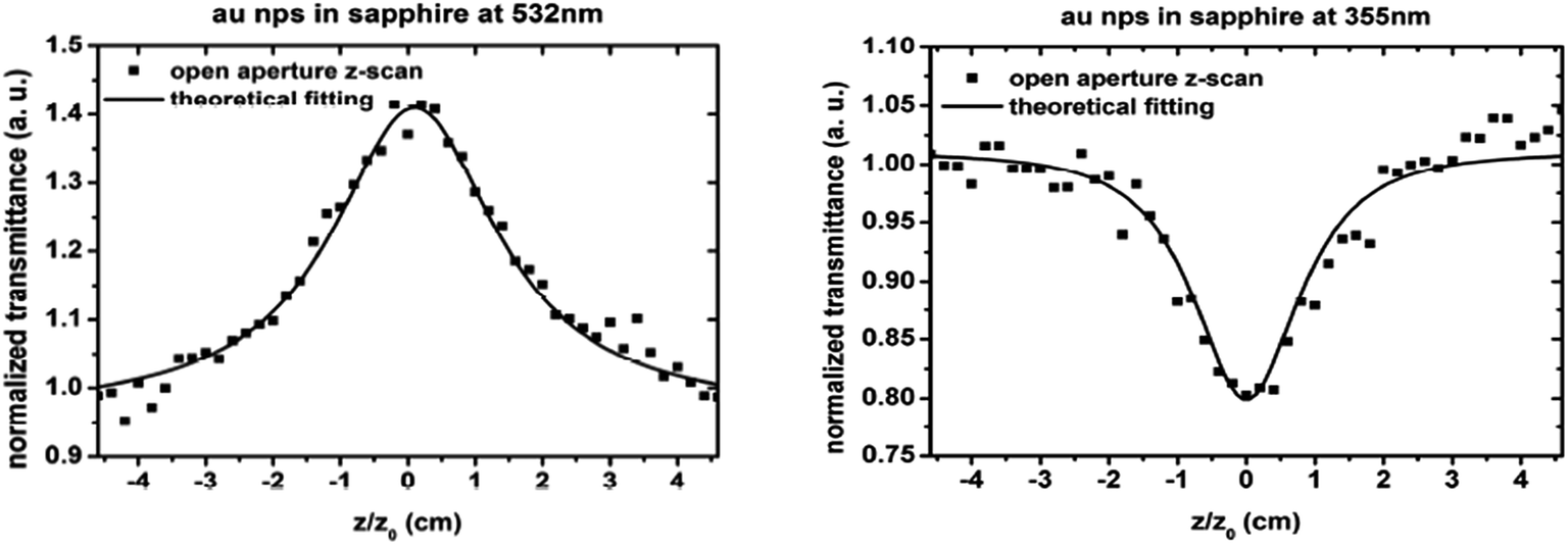 | ||
| Fig. 3 Nonlinear absorption values for the isotropic Au NPs in α-Al2O3 at 532 nm and 355 nm. For the first wavelength, the nonlinear optical absorption is negative, whereas it is positive for the second wavelength.41 | ||
 | ||
| Fig. 4 Nonlinear refraction for the isotropic Au NPs in α-Al2O3 at 532 nm and 355 nm. For the first wavelength, the nonlinear optical refraction is positive, whereas it is null for the second wavelength.41 | ||
Analysis of the absorption spectra of gold nanoparticles in three matrices showed that the SPR of gold nanoparticles was located in the region of 525 nm for Al2O3,47 540 nm for ZnO,48 and 500 nm for SiO2.49 The values of the absorption coefficient reported for the matrices under consideration were 3.3 × 10⁻¹⁶ cm2 W−1 for Al2O3, −9 × 10⁻¹⁵ cm2 W−1 for ZnO,50 and 2.24 × 10⁻¹⁶ cm2 W−1 for SiO2 (ref. 51) at the wavelength of 532 nm. These data were much smaller than those of the composite materials. Thus, it could be concluded that the nonlinear optical response of the composites was derived from the gold nanoparticles.
2.2 Nonlinear optical studies of silicon-based materials
Silicon-based optical devices have received significant attention because of their potential application in high-speed signal processing and no-chip communications.52 The NOPs of silicon have been studied for a long time and have been subsequently characterized with various different techniques; this has resulted in a large range of reported data.53 The accuracies of these studies were quite essential, which were used to characterize the linear coupling and propagation losses. The nonlinear optical properties of silicon have been utilized in the design of modulators, receivers, and filters in optical communication demonstrations with bit rates in the order of 1 Tbits per s (ref. 54) and in real-time A-to-D converters with the sampling rates of several tens of Gbits per s. A major advantage of the silicon photonic devices is that they can be produced efficiently because of the superiority of the mature silicon processing technology that has been extensively developed to permit low-cost, large-volume electronic circuit production. This makes optical devices compatible with the CMOS technology possible for on-chip integration. The high bandwidths, high speeds, and energy efficiency of optical communication circuits allow on-board communication with performances greatly surpassing those of the electronic alternative.55Si and SiO2 multilayers with a dot size of 2.5 nm were prepared, and their microstructures were characterized by cross-sectional transmission microscopy and Raman spectroscopy. A broad photoluminescence band centered at 870 nm was observed. The multi-layer nonlinear optical effect was studied by the Z-scanning technique under the excitation of two laser pulses. Photoluminescence at room temperature was observed at 870 nm; the large Stokes shift between the linear absorption edge and emission band implied that the emission might originate from the recombination of photoexcited carriers via interface states with an energy level inside the gap.56
In Table 2, the nonlinear absorption coefficient and nonlinear refractive index of the sample upon changing the excitation pulse time from ps to fs are shown. When the sample was excited by a picosecond laser, it showed saturation absorption with β = −3.1 × 10⁻⁶ cm W−1 and n2 = −1.3 × 10⁻¹⁰ cm2 W−1. The negative nonlinear refraction could be attributed to the free carrier dispersion effect. The saturation absorption can be attributed to the single photon transition process between the valence band and the interface state. However, when the sample was excited by a femtosecond laser, the sample showed reverse saturation absorption with β = 1.1 × 10⁻⁷ cm W−1 and n2 = −1.5 × 10⁻¹² cm2 W−1. The difference in the free carrier density generated by two pulses laser played a great role in the diverse nonlinear response.
| Excitation pulse duration | Nonlinear absorption coefficient (β)/(cm W−1) | Nonlinear refractive index (n2)/(cm2 W−1) |
|---|---|---|
| Picosecond laser (ps) | −3.1 × 10⁻⁶ | −1.3 × 10⁻¹⁰ |
| Femtosecond laser (fs) | 1.1 × 10⁻⁷ | −1.5 × 10⁻¹² |
A tunable nonlinear absorption and nonlinear refraction response in Si/SiO2 multilayers have been observed during the transition process from the amorphous to nanocrystalline phases under femtosecond excitation at 800 nm by Zhang et al.57 They suggested that the two-photon absorption process dominates in the samples mainly containing amorphous Si phases, whereas the phonon-assisted one-photon transition process between the valence band and interface states dominates the nonlinear optical properties in nc-Si/SiO2 multilayers. This suggests that nc-Si/SiO2 multilayers can be applied in highly sensitive photonic devices such as optical switches and Q-switch lasers.
Silicon nanocrystals are widely used in photonics, with their most important characteristics being two aspects: (1) they can be used as a nonlinear material in various devices, e.g., in bistable optical cavities, in waveguide optical mode monitors based on two-photon excited luminescence detection, and in wavelength shifters using four-wave mixing; (2) they can be used as an entropy source for quantum random number generation, which is the key device for cryptography. Quantum size effects change the properties of Si-nc with respect to bulk silicon; this allows enlargement of the phenomenology and the application spectrum of silicon photonics.58
2.3 Nonlinear optical studies of Ag
Due to their large third-order nonlinear optical properties caused by surface plasmon resonance and the quantum size effect, noble metallic nanostructures embedded on a transparent dielectric matrix have been attracting significant attention59,60 as promising materials for all-optical signal processing devices.61,62 Consequently, a few technologies have been developed such as laser ablation,63,64 chemical synthesis, ion implantation,65–67 and sol–gel methods. The quantum size effect will make the material show a more excellent performance, different from that of other noble metallic NPs, and silver NPs experience a lower intrinsic loss of plasmonic energy at visible frequencies that gives rise to SPR.68 Moreover, in further research, it has been indicated that the shape of the metallic NPs and their dielectric environment determine the surface frequency and consequently the nonlinear optical properties.65,69,70NF-RGO (non-covalent functionalized reduced graphene oxide) and NF-RGO/Ag-NPs (NF-RGO decorated with various concentration of silver nanoparticles) were prepared by Sakho et al.71 The open aperture Z-scan technique was used to investigate the nonlinear optics. Tables 3 and 4 show the numerical calculated values of the nonlinear optical parameters at λ = 800 nm with femtosecond and λ = 532 nm with nanosecond excitation regimes, respectively. The lower optical limiting threshold was attributed to the charge or energy transfer between NF-RGO and Ag-NPs in the NF-RGO/Ag-NP hybrid. In nonlinear optical absorption, the lower the optical threshold value, the better the optical limiting properties.
| Samples | β (10−15 m W−1) | Is (1016 W m−2) | Optical limiting threshold (J cm−2) |
|---|---|---|---|
| NF-RGO | 2.5 | 3.5 | 1.6 |
| NF-RGO/Ag-NPs (0.1 M) | 6.7 | 2.5 | 1.7 |
| NF-RGO/AgNPs (0.3 M) | 6.0 | 2.5 | 1.7 |
| NF-RGO/AgNPs (0.5 M) | 4.8 | 3.9 | 1.7 |
| NF-RGO/AgNPs (1 M) | 5.8 | 3.5 | 1.6 |
| Samples | β (10−10 m W−1) | Is (1011 W m−2) | Optical limiting threshold (J cm−2) |
|---|---|---|---|
| NF-RGO | 2.8 | 3.8 | 8.3 |
| NF-RGO/AgNPs (0.1 M) | 7.99 | 4 | 4.3 |
| NF-RGO/AgNPs (0.3 M) | 7.99 | 3.8 | 5.9 |
| NF-RGO/AgNPs (0.5 M) | 7.99 | 3.7 | 7.2 |
| NF-RGO/AgNPs (1 M) | 13.9 | 2.8 | 8.1 |
In the fs regime, β was found to increase with the decreasing concentration of AgNPs. The higher the β value, the better the OL properties of the corresponding material. In addition, in the fs regime, the samples exhibited the same optical limiting behavior as in the ns regime. The optical limiting thresholds were found to be lower in the fs excitation regime as compared to those in the ns excitation regime. This was attributed to the prominent plasmon band bleaching of AgNPs when excited at 532 nm. Furthermore, the nonlinear optical analyses showed that the optical properties of the NF-RGO/Ag-NP hybrid were size dependent. This finding provided a good understanding of the graphene-based nonlinear materials and also indicated that the as-synthesized materials could be potential candidates for optical limiting applications. Moreover, Li et al.68 have observed that the nonlinear absorption coefficients significantly depend on the excitation energy and can be modulated by varying the fluence of Ag+ ions.
3 NOPs of components synthesized by different methods
3.1 Vacuum electron-beam co-evaporation method
In the past few decades, the nanostructures of direct band gap semiconductors, such as Si and Ge, have been extensively studied because of their potential applications in nanophotonics, with their main advantage being their compatibility with conventional integrated circuit technology. Amorphous and crystallized Ge nanostructures embedded in an Al2O3 dielectric were synthesized by a vacuum electron-beam co-evaporation method.72 A clear blue-shift of the absorption edge and a large third-order nonlinear optical susceptibility due to the quantum confinement effect were observed.Herein, three samples with different Ge concentrations ((A) Ge/Al2O3 = 1/5, (B) Ge/Al2O3 = 2/5, and (C) Ge/Al2O3 = 5/5) were synthesized, and the thickness was about 200 nm. The band gap of the semiconductor was increased due to the quantum confinement effect, which caused a blue-shift of the absorption band edge and optical luminescence.73,74 Moreover, this effect caused an enhancement of the third-order optical nonlinearity. Optical absorption measurements were performed in the visible to near-infrared range at room temperature. Fig. 5 shows the optical absorption spectra of Ge + Al2O3 films on quartz substrates. It was clear that all these samples exhibited a blue-shift of the band gap because the band gap of the bulk amorphous Ge (α-Ge) was about 0.9 eV. According to the indirect transition equation,
| α(hν) = α(hν − Eg)2/ν | (11) |
 | ||
| Fig. 5 Optical absorption spectra of Ge nanocrystals embedded in Al2O3 films on quartz substrates (synthesized at room temperature; thickness: 200 nm).72 | ||
The third-order nonlinear optical characteristics of sample A were determined by the Z-scan method at a wavelength of 532 nm and a pulse width of 10 ns. The closed aperture plot (Fig. 6(a)) shows a distinct valley-peak configuration typical of the positive nonlinear effects (self-focusing). The nonlinear optical refractive index n2 defined as
| n = n0 + n2I | (12) |
| n2 (m2 W−1) = 1.232λτω02ΔTP-V/(1 − s)0.25LeffE | (13) |
 | ||
Fig. 6 Z-Scan plots of the Ge nanocrystals embedded in an Al2O3 film (Ge![[thin space (1/6-em)]](https://www.rsc.org/images/entities/char_2009.gif) :Al2O3 = 1:5): (a) closed aperture and (b) open aperture. The solid curves are the theoretical fits.72 :Al2O3 = 1:5): (a) closed aperture and (b) open aperture. The solid curves are the theoretical fits.72 | ||
3.2 Melt-quenching technique
Glasses containing metal nanoparticles exhibit an ultrafast electron response within a few of picoseconds, which also have large third-order optical nonlinearities for a large local-field enhancement factor and strong resorption of the surface plasmon.75–77 Thus, these materials have been intensively studied in the last few decades as they are widely used in ultrafast all-optical switching, ultrafast imaging, optical telecommunications, signal processing, and so on.78,79 Glasses containing metal nanoparticles are generally fabricated by melt quenching, the sol–gel method, sputtering, ion exchange, ion implantation, or femtosecond laser irradiation.80–82 It is typically really difficult to control Bi nanoparticles formation in glasses. Thus, Lin et al.83 proposed a simple method, whereby they used Al to reduce Bi ions to atomic state Bi, and the atomic or molecular Bi gathered together. Bi grows and forms nanocrystals during the subsequent heat treatment. The Z-scan technique was used to investigate the nonlinear optical properties of the Bi nanoparticle composite glasses.Typical Z-scan normalized transmittance curves for open and closed aperture measurements of these Bi glasses are shown in Fig. 7. The nonlinear index γ, nonlinear refractive index n2, nonlinear absorption coefficient β, and third-order optical susceptibility χ(3) of all the samples were obtained by applying nonlinear curve fitting, and the obtained third-order optical nonlinearities are shown in Table 5. It can be found that the third-order optical susceptibility χ(3) increases as the heat treatment temperature increases.
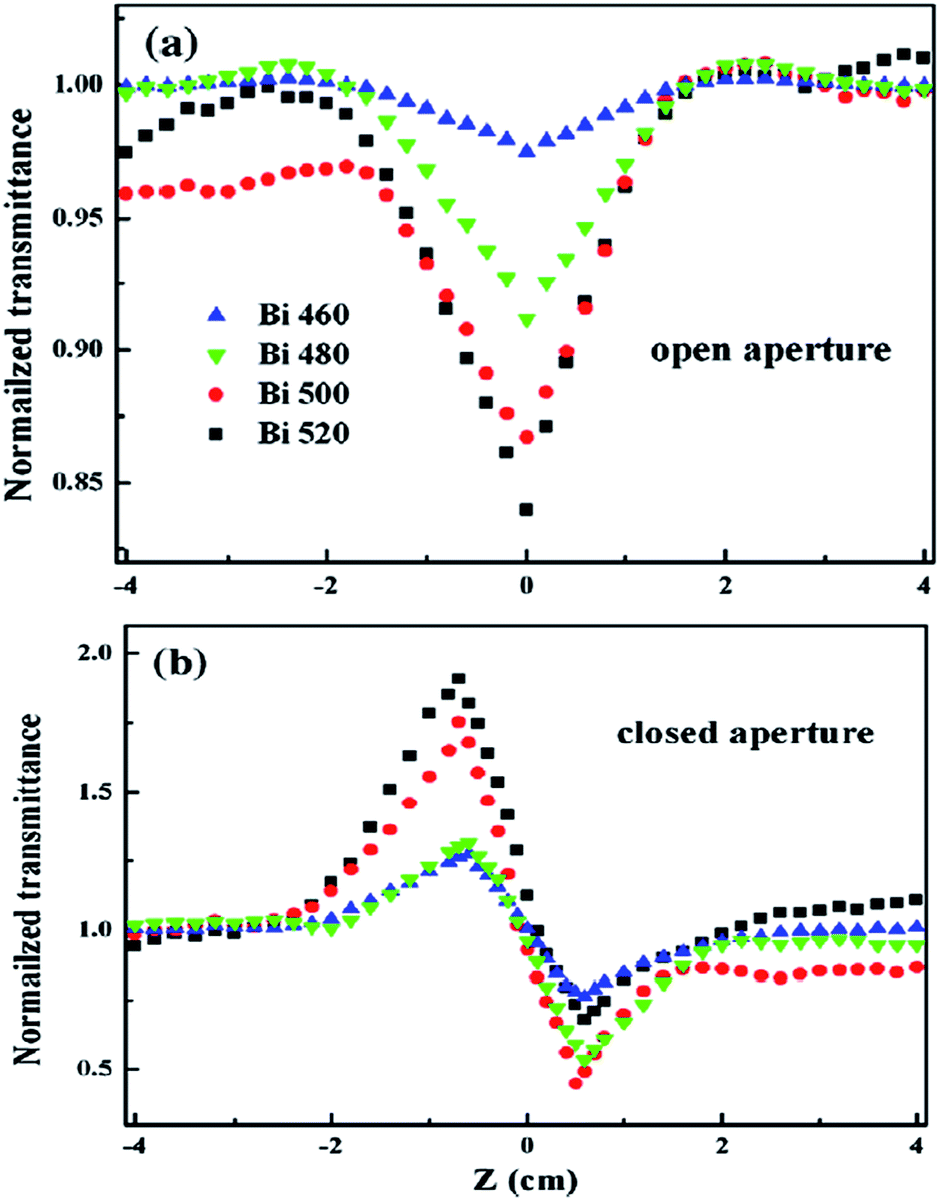 | ||
| Fig. 7 Typical Z-scan normalized transmittance curves for (a) open and (b) closed aperture measurements.83 | ||
| Sample | n2 (10−9 esu) | β (cm GW−1) | χ(3) (10−7 esu) |
|---|---|---|---|
| Bi 460 | 0.68 | 0.82 | 0.39 |
| Bi 480 | 1.78 | 3.99 | 1.01 |
| Bi 500 | 3.42 | 6.66 | 1.95 |
| Bi 520 | 4.37 | 9.54 | 2.49 |
3.3 Nanosphere lithography
A systematic study of the size-related nonlinear optical properties of triangular Au particles was reported, where triangular Au nanoparticle arrays with four sizes (37 nm, 70 nm, 140 nm, and 190 nm) were fabricated on SiO2 substrates using nanosphere lithography. There are many ways, such as chemical methods84–86 and sputtering method,87 to fabricate particles of different sizes. Nanosphere lithography has been developed from natural lithography by Hulteen et al.88 in 1995 and proven to be a powerful tool to fabricate periodic particle arrays (PPAs) with a tunable shape and size, which has made it possible to quantitatively study the optical properties of nanoparticles (Table 6).| Size (nm) | α0 (cm−1) | β (cm GW−1) | n2 (cm2 GW−1) | W | T |
|---|---|---|---|---|---|
| 37 | 1.4 × 10³ | 54 | −0.035 | 7.5 | 0.12 |
| 70 | 1.5 × 10³ | 29 | −0.032 | 5.6 | 0.07 |
| 140 | 1.5 × 10³ | 5 | 0.17 | 4.5 | 0.02 |
| 190 | 1.7 × 10³ | 0 | 0.02 | 4.1 | 0 |
Fig. 8 shows the absorption spectra of Au PPAs of different sizes. It can be seen that the absorption peaks due to the SPR of Au particles are located at 552 nm, 566 nm, 580 nm, and 606 nm for the 37 nm, 70 nm, 140 nm, and 190 nm sizes, respectively. With the increasing particle size, the absorption peak shifts to longer wavelength, and when λ = 800 nm, the linear absorption coefficient significantly increases. These size-related linear absorption properties lead to competition between two nonlinear mechanisms: the interband transition through the dominant two-photon absorption (TPA) process and the intraband contribution ascribed to the saturated absorption (SA) process with excitation at the edge of the SPR band for λ = 800 nm.89
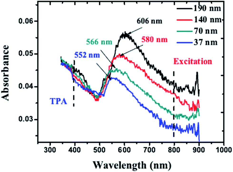 | ||
| Fig. 8 Absorption spectra of Au periodic particle arrays with SPR peaks at 552 nm, 566 nm, 580 nm, and 606 nm. As the sizes increase, the SPR peaks shift to the longer wavelength.89 | ||
Fig. 9 shows the typical OA results of the four samples. The black dots indicate the experimental data and the solid lines present the theoretical fits. The laser intensities were calculated to be 55 GW cm−2 by I0 = E0/πω2τ. At the repetition rate of 1 kHz, the accumulative thermal effects can be neglected. The curve of the 37 nm-sized sample showed a TPA process with an additional SA component. For the curves of the samples sized 70 nm and 140 nm, the TPA component turned weaker and SA became dominant. The curve of the 190 nm sized sample showed only the SA component. The differences are because the absorption in the excitation region is much weaker than that at 400 nm for the Au PPA sized 37 nm, and herein, the interband to the TPA process plays a key role. However, the absorption at 800 nm is larger than that at 400 nm for the Au PPA sized 190 nm; this is because the SA process becomes dominant. The curves of the samples sized 70 nm and 140 nm showed a transition in this variation of the two nonlinear mechanism contributions.
 | ||
| Fig. 9 The OA Z-scan results of 4 samples at the exciting intensities at the focal point I0 = 55 GW cm−2. The solid lines show the theoretical best fit.89 | ||
Fig. 10 shows the CA Z-scan data for the Au PPAs at I0 = 55 GW cm−2. For the Au PPAs sized 37 nm and 70 nm, a self-defocusing effect occurs, where the sign of nonlinear refraction is negative. For the Au PPAs sized 140 nm and 190 nm, self-defocusing occurs, with a positive nonlinear refraction. For the Au PPAs sized 37 nm and 70 nm, the nonlinear refraction index decreases due to the dominant interband transition caused by the TPA process. As the particle size increases, the SA process becomes dominant. The refractive index increases due to the excited electrons; this results in self-focusing. It is worth nothing that there are two clear deviations from the theoretical values of data for the 70 nm sized sample; this indicates a transition process from self-defocusing to self-focusing (Table 7).
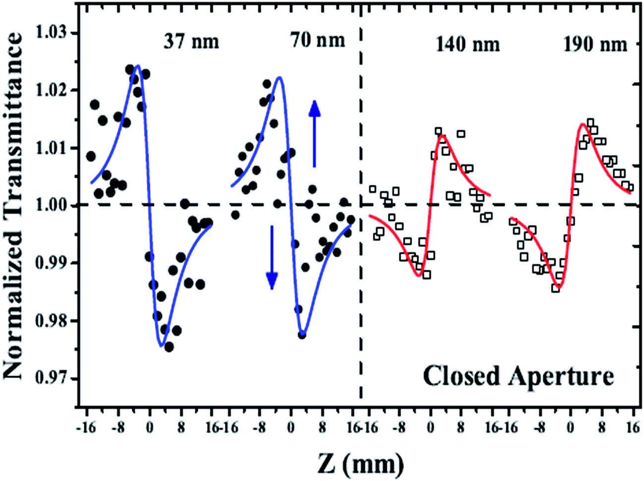 | ||
| Fig. 10 The CA Z-scan results of the 4 samples at exciting intensities at the focal point I0 = 55 GW cm−2. The solid lines show the theoretical best fit.89 | ||
| CdSe size (nm) | α0 (cm−1) | Leff (cm) | β (10−10 m W−1) | Im χ(3) (10−12 esu) |
|---|---|---|---|---|
| 3.37 | 3.77 | 0.18 | 9.8 | 24 |
| 3.54 | 4.07 | 0.17 | 8.5 | 20 |
| 3.91 | 4.72 | 0.16 | 5.0 | 12 |
| 4.56 | 4.49 | 0.16 | 1.8 | 4.3 |
| 5.07 | 3.34 | 0.19 | 1.4 | 3.4 |
3.4 Organometallic pyrolysis method
In recent years, the NOPs of nanoparticles have attracted significant interest due to their various applications in optoelectronic and biological fields such as in optical limiting,90,91 multiphoton imaging,92,93 all-optical switching,94,95 cell biology, and cancer-therapy.96–98 The combination of nanometals and semiconductors has acquired particular interest for basic sciences and technological applications.99,100In the study reported by Salah et al.,101 Au NPs and nanocomposite of Au–CdSe of different NPs sizes and concentrations were prepared.
The effect of the nanosize of CdSe on the nonlinear absorption was investigated, as shown in Fig. 11. At the excitation intensities I0 = 118 μJ, the transmission via NPs of different sizes increases near the focus beam (z = 0). This is an indication that the absorption of the ground state is higher than that of the excited states. The SA decreases as the QDs size increases. This decrease can be clearly seen in Table 8, where the nonlinear absorption coefficients are summarized together with different parameters used in the fitting process. This decrease is attributed to the decrease in absorption associated with the increase in the QD size.
 | ||
| Fig. 11 OA Z-scan of Au–CdSe of different sizes and excitation intensities I0 = 118 μJ.101 | ||
| Conc. ratio of QDs sized 3.54 nm | α0 (cm−1) | Leff (cm) | β (10−10 m W−1) | Im χ(3) (10−12 esu) |
|---|---|---|---|---|
| 1/2.5 | 12.43 | 0.079 | 29 | 69.9 |
| 1/5 | 6.72 | 0.13 | 12.7 | 30.5 |
| 1/10 | 4.04 | 0.17 | 4.96 | 11.9 |
| 1/20 | 2.16 | 0.22 | 2.19 | 5.26 |
| 1/40 | 1.16 | 0.25 | 0.908 | 2.19 |
| 1/80 | 0.61 | 0.27 | 0.311 | 0.075 |
The effect of the concentrations of NPs on the nonlinear absorption behavior of NPs was examined, as shown in Fig. 12. OA Z-scan transmissions at a laser energy of 195 μJ (0.31 GW cm−2) were carried out for different concentrations of Au–CdSe at CdSe QDs sized 3.54 nm. The observed SA nonlinear behavior was found to increase as the concentration of NPs increased. The variation in the calculated nonlinear absorption coefficients of Au–CdSe at different concentrations is summarized in Table 8.
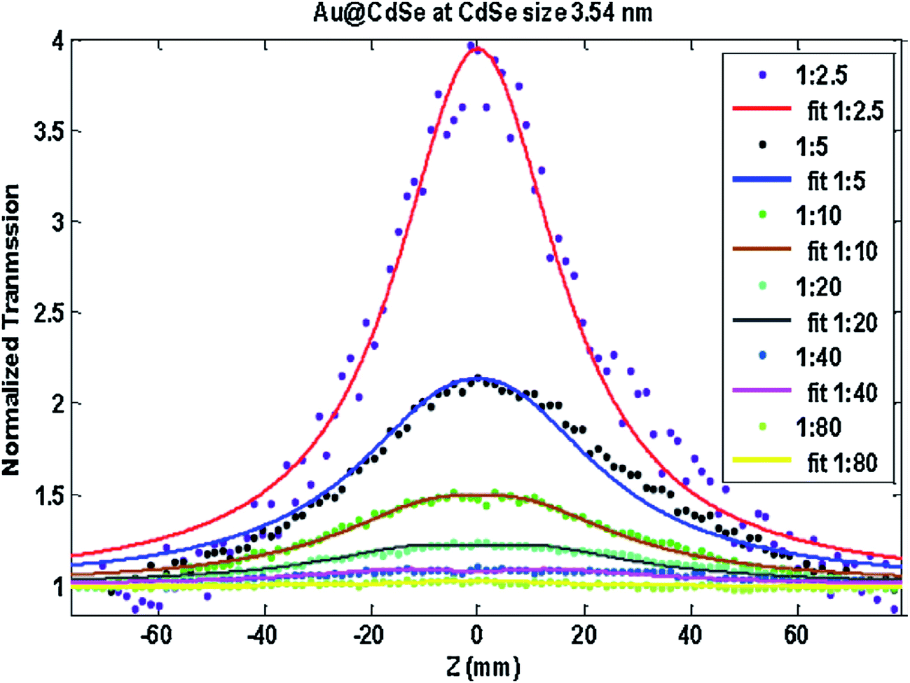 | ||
| Fig. 12 OA Z-scan transmission of Au–CdSe at 0.31 GW cm−2 for different concentrations of CdSe (3.54 nm).101 | ||
3.5 Colloidal chemical synthesis
Among the II–VI semiconductors, CdSe is one of the promising semiconducting materials that has been studied for application in solar cells,102 thin film transistors,103 gamma-ray detectors,104 memory devices,105 and optoelectronic106 and biological applications.107 Polymer nanocomposites (PNCs) are a class of relatively new materials with ample potential applications. Herein, the pure CdSe PNC was marked as sample A. Ag–CdSe hybrid PNC was prepared via a colloidal chemical synthesis technique by mixing the required amounts of Ag colloids with CdSe PNC.108 The volume fraction of Ag was changed by keeping the volume of CdSe PNC constant. The prepared nanocomposite samples had the composition Ag(x)–CdSe PNC, with x = 0.1, 0.2, and 0.3%, and these samples were marked as B, C, and D, respectively. The nonlinear optical properties of the nanocomposite thin films were investigated using the Z-scan technique with a 2 mW CW He–Ne laser operating at 632.8 nm.Thermo-optical coefficient (dn/dT) was calculated using the following relation:109
 | (14) |
| Sample | α (cm−1) | β (×10−6 m W−1) | n2 (×10−9 m2 W−1) | χ(3) (×10−10 m2 V−2) | dn/dT (×10−8 K−1) |
|---|---|---|---|---|---|
| A | 449 | 1.51 | 3.02 | 1.88 | 3.8 |
| B | 553 | 1.77 | 5.31 | 4.48 | 5.4 |
| C | 629 | 1.85 | 8.87 | 9.45 | 7.9 |
| D | 706 | 1.74 | 9.08 | 11.23 | 7.3 |
4 Conclusions
Nonlinear optics was established soon after the invention of the laser in 1960. It has a long development history of about half a century, and its research field has been continuously developing in depth and breadth. Nonlinear optics studies involve various kinds of nonlinear effects in the interactions between a laser and matter; the research contents include two aspects: one is the study of how to change the macroscopic parameters, such as susceptibility, dielectric coefficient, refractive index, and absorption coefficient, of the matter in the laser with an aim to realize the control of matter by light. The other aspect involves study of how pump-laser-induced matter changes can affect the parameters, such as frequency, power, wave vector, pulse, pulse width, and propagation direction, of the signal light propagating in the matter, with an aim to realize control of light with light. To date, nonlinear optics has gained extensive applications. For example, it has been widely used in laser technology to change the frequency of the laser and compress the pulse width of the laser; it has also been used to fabricate various optoelectronic devices such as lasers, optical amplifiers, and optical storage and optical switches; it has made an important contribution to the development of nonlinear optical communications and space optical communication; it has been using the nonlinear optical limiting technology to fight against the blinding laser weapons; the nonlinear optics is a useful tool for new materials; and it is also a necessary tool for measuring the nonlinear optical parameters of materials. Devices based on nonlinear optics are compatible with quantum memories and fiber optic communications, as well as with silicon integrated circuit semiconductor technology. These new developments can play a key role in realizing compact, low-cost, and practical sources of complex quantum optical states on a chip, which will ultimately enable quantum technologies to have a significant impact on our society.There are several different methods and techniques for determining the nonlinear optical response of a material. Z-Scan is one of the simpler experimental methods to be employed and interpreted. Although there are plenty of available methods, it is rare that any single experiment will completely determine the physical processes behind the nonlinear response of a given material. Z-Scan has only recently been introduced. The use of the Z-scan technique as both an absolutely calibrated method for determining standards and as a relative measurement method is increasing. The Z-scan signal can provide useful information on the order of the nonlinearity as well as its sign and magnitude.
Ion implantation has been proven in recent studies as a reliable technique to tune the properties of bulk materials, thin films, nanostructure materials, and biocompatible materials for specific applications. However, the material properties can be altered depending on the proper selection of ion species, ion energy, substrate temperature, and ion fluencies. Compared to other techniques for modifying the surface of the material, ion implantation can obtain the specified characteristics that are needed; therefore, it has wider application prospects. Organic and inorganic composite nonlinear optical materials will likely become a new development trend for nonlinear optical materials due to the powerful theory and technical feasibility behind them. With continuous study, if some problems can be better solved, such as external electric field polarization and the organic and inorganic composite temperature contradiction, a number of high efficiency, high strength, and fast response materials will be developed. This will also support further development of nonlinear optics with regard to device development and theoretical research.
Conflicts of interest
There are no conflicts to declare.Acknowledgements
This work was supported by the National Natural Science Foundation of China (No. 11375136) and Program for Outstanding Young Science and Technology Innovation Teams in Higher Education Institutions of Hubei Province, China (No. T201502).References
- R. W. Boyd and B. R. Masters, Nonlinear optics, J. Biomed. Opt., 2009, 14(2), 029902 CrossRef.
- S. R. Marder, J. E. Sohn and G. D. Stucky. Materials for Nonlinear Optics Chemical Perspectives.; ACS Symp. Ser., American Chemical Society, 1991 Search PubMed.
- S. S. Zahraa, S. A. Raad and J. T. Khawla, Study of the Nonlinear Optics Properties of Lithium Triborate Crystal by Using Z-Scan Technique, Int. J. Sci. Res., 2016, 1683–1687 Search PubMed.
- P. A. Franken, A. E. Hill and C. W. Peters, et al., Generation of Optical Harmonics, Phys. Rev. Lett., 1961, 7(4), 118–119 CrossRef.
- T. H. Maiman, Stimulated Optical Radiation in Ruby, Nature, 1960, 187(4736), 493–494 CrossRef.
- C. G. Schroer and B. Lengeler, Handbook of Lasers and Optics, 2012, pp. 1461–1474 Search PubMed.
- R. L. Byer and A. Piskarskas, Optical Parametric Oscillation and Amplification Introduction, J. Opt. Soc. Am. B, 1993, 10(3), 2148 CrossRef.
- G. A. Askar'Yan, The self-focusing effect, Phys.-Usp., 1973, 16(5), 680 CrossRef.
- D. W. Forslund, J. M. Kindel and E. L. Lindman, Theory of stimulated scattering processes in laser-irradiated plasmas, Phys. Fluids, 1975, 18(8), 1002–1016 CrossRef.
- U. Kreibig and M. Vollmer. Optical Properties of Metal Clusters[M]//Optical properties of metal clusters/, Springer-Verlag, 1995, pp. 278–279 Search PubMed.
- B. Raneesh, I. Rejeena and P. U. Rehana, et al., Nonlinear optical absorption studies of sol–gel derived Yttrium Iron Garnet (Y3Fe5O12) nanoparticles by Z-scan technique, Ceram. Int., 2012, 38(3), 1823–1826 CrossRef CAS.
- J. U. Seongmin, P. R. Wateker and S. Jeong, et al., Nonlinear optical properties of Zinc doped germane-silicate glass optical fiber, J. Nonlinear Opt. Phys. Mater., 2011, 19(04), 791–799 Search PubMed.
- Y. Wang, C. Y. Lin and A. Nikolaenko, et al., Four-wave mixing microscopy of nanostructures, Adv. Opt. Photonics, 2010, 3(1), 1–52 CrossRef.
- P. Ren, H. Fan and X. Wang, Electrospun nanofibers of ZnO/BaTiO3, heterostructures with enhanced photocatalytic activity, Catal. Commun., 2012, 25(8), 32–35 CrossRef CAS.
- S. Krishnan, C. S. S. Sandeep and R. Philip, et al., Two-photon assisted excited state absorption in multiferroic YCrO3, nanoparticles, Chem. Phys. Lett., 2012, 529(5), 59–63 CrossRef CAS.
- S. Hu, C. Melton and D. Mukherjee, A facile route for the synthesis of nanostructured oxides and hydroxides of cobalt using laser ablation synthesis in solution (LASIS), Phys. Chem. Chem. Phys., 2014, 16(43), 24034–24044 RSC.
- S. Basak and R. Chandrasekar, Passive optical waveguiding organic rectangular tubes: tube cutting, controlling light propagation distance and multiple optical out-puts, J. Mater. Chem. C, 2013, 2(8), 1404–1408 RSC.
- A. V. Emelyanov, M. V. Khenkin and A. G. Kazanskii, et al., Femtosecond laser induced crystallization of hydrogenated amorphous silicon for photovoltaic applications, Thin Solid Films, 2014, 556(4), 410–413 CrossRef CAS.
- R. Udayabhaskar, M. S. Ollakkan and B. Karthikeyan, Preparation, optical and non-linear optical power limiting properties of Cu, CuNi nanowires, Appl. Phys. Lett., 2014, 104(1), 958 CrossRef.
- T. Jiang, G. Qin and W. Qin, et al., Passively Q-switched erbium-doped fiber laser based on gold nanorods, Optik, 2014, 125(19), 5789–5793 CrossRef CAS.
- C. Tang, Q. Zheng and H. Zhu, et al., Two-photon absorption and optical power limiting properties of ladder-type tetraphenylene cored chromophores with different terminal groups, J. Mater. Chem. C, 2013, 1(9), 1771–1780 RSC.
- H. Fan, X. Wang and Q. Ren, et al., Investigation of the nonlinear absorption and optical limiting properties of two [Q][Cu(CS)] compounds, Opt. Laser Technol., 2010, 42(5), 732–736 CrossRef CAS.
- L. W. Tutt and T. F. Boggess, A review of optical limiting mechanisms and devices using organics, fullerenes, semiconductors and other materials, Prog. Quantum Electron., 1993, 17(4), 299–338 CrossRef CAS.
- K. N. Chopra, A short note on technical analysis of excimer lasers, their optimization for laser corneal refractive surgery, and novel applications, Latin-American Journal of Physics Education, 2014, 8 Search PubMed.
- N. Pisitpipathsin, P. Kantha and K. Pengpat, et al., Effect of KNbO3, on physical and electrical properties of lead-free BaTiO3, ceramic, Ceram. Int., 2015, 41(3), 3639–3646 CrossRef CAS.
- A. L. Stepanov, Laser annealing of composite materials with metal nanoparticles[M]//high-power and femtosecond lasers, in High-Power and Femtosecond Lasers, ISBN 978-1-60741-009-6, 2009, pp. 27–70 Search PubMed.
- L. Nicolais and G. Carotenuto, Metal-Polymer Nanocomposites, Mater. Today, 2005, 8(2), 174–182 Search PubMed.
- F. Gonella and P. Mazzoldi, Handbook of Nanostructured Materials & Nanotechnology, 2000, vol. 4, ch. 2–Metal nanocluster composite glasses, pp. 81–158 Search PubMed.
- A. L. Stepanov, Ion-synthesis of silver nanoparticles and their optical properties, Langmuir, 2010, 26(6), 4176–4183 CrossRef PubMed.
- U. Kreibig and M. Vollmer. Optical Properties of Metal Clusters[M]//Optical Properties of Metal Clusters/, Springer-Verlag, 1995, pp. 278–279 Search PubMed.
- D. Ricard, P. Roussignol and C. Flytzanis, Surface-mediated enhancement of optical phase conjugation in metal colloids., Opt. Lett., 1985, 10(10), 511–513 CrossRef CAS PubMed.
- M. Sheik-Bahae, A. A. Said and E. W. Van Stryland, High-sensitivity, single-beam n(2) measurements, Opt. Lett., 1989, 14(17), 955 CrossRef CAS PubMed.
- M. Sheik-Bahae, D. J. Hagan and E. W. Van Stryland, Dispersion and band-gap scaling of the electronic Kerr effect in solids associated with two-photon absorption, Phys. Rev. Lett., 1990, 65(1), 96 CrossRef CAS PubMed.
- W. P. Zang, J. G. Tian and G. Y. Zhang, et al., Theoretical analysis of Z-scan in thick optical nonlinear media, Acta Phys. Sin., 1994,(3), 476–482 CAS.
- A. Cetin, R. Kibar and M. Hatipoglu, et al., Third-order optical nonlinearities of Cu and Tb nanoparticles in SrTiO3, Phys. B, 2010, 405(9), 2323–2325 CrossRef CAS.
- S. J. Wagner, B. M. Holmes and U. Younis, et al., Controlling Third-Order Nonlinearities by Ion-Implantation Quantum-Well Intermixing, IEEE Photonics Technol. Lett., 2009, 21(2), 85–87 CrossRef CAS.
- M. Bayle, C. Bonafos and P. Benzo, et al., Ag doped silicon nitride nanocomposites for embedded plasmonics, Appl. Phys. Lett., 2015, 107(10), 101907 CrossRef.
- Y. H. Wang, S. J. Peng and J. D. Lu, et al., Nonlinear optical properties of Ag nanocluster composite fabricated by 200 keV negative ion implantation, Vacuum, 2008, 83(2), 412–415 CrossRef CAS.
- T. Cesca, G. Pellegrini and V. Bello, et al., Nonlinear optical properties of Au-Ag nanoplanets made by ion beam processing of bimetallic nanoclusters in silica, Nucl. Instrum. Methods Phys. Res., 2010, 268(19), 3227–3230 CrossRef CAS.
- M. Song, Q. M. Liu and G. X. Cai, et al., Enhancement of third-order optical nonlinearities in 72GeS2–18Ga2S3–10CdS glasses by Ag ion implantation, Chalcogenide Lett., 2015, 12(9), 453–460 CAS.
- O. Sánchezdena, P. Motasantiago and L. Tamayorivera, et al., Size-and shape-dependent nonlinear optical response of Au nanoparticles embedded in sapphire, Opt. Mater. Express, 2013, 4(1), 92 CrossRef.
- A. I. Ryasnyanskiy, B. Palpant and S. Debrus, et al., Third-order nonlinear-optical parameters of gold nanoparticles in different matrices, J. Lumin., 2007, 127(1), 181–185 CrossRef CAS.
- J. W. Chen, Q. Ren and X. Q. Wang, et al., Third-Order Nonlinear Optical Properties of 1,3-Dithiole-2-thione-4,5-dithiolate Compounds at Different Wavelengths, Acta Phys.-Chim. Sin., 2012, 28(4), 942–948 CAS.
- C. Torres-Torres, A. López-Suárez and B. Can-Uc, et al., Collective optical Kerr effect exhibited by an integrated configuration of silicon quantum dots and gold nanoparticles embedded in ion-implanted silica, Nanotechnology, 2015, 26(29), 295701 CrossRef CAS PubMed.
- A. Agrawal, T. Ahmad Dar and R. Solanki, et al., Study of nonlinear optical properties of pure and Mg-doped ZnO films, Phys. Status Solidi, 2015, 252(8), 1–6 Search PubMed.
- Z. Chai, Y. Zhi and L. Liu, et al., Effect of absorption on the diffraction efficiency in Fe:LiNbO3 crystal with 90° recording geometry, J. Opt. A: Pure Appl. Opt., 2005, 7(12), 711 CrossRef CAS.
- A. Dakka, J. Lafait and C. Sella, et al., Optical properties of Ag–TiO2 nanocermet films prepared by cosputtering and multilayer deposition techniques, Appl. Opt., 2000, 39(16), 2745 CrossRef CAS PubMed.
- U. Pal, E. A. Almanza and O. V. Cuchillo, et al., Preparation of Au/ZnO nanocomposites by radio frequency co-sputtering, Sol. Energy Mater. Sol. Cells, 2001, 70(3), 363–368 CrossRef CAS.
- N. Pinçon, B. Palpant and D. Prot, et al., Third-order nonlinear optical response of Au:SiO2, thin films: Influence of gold nanoparticle concentration and morphologic parameters, Eur. Phys. J. D, 2002, 19(3), 395–402 CrossRef.
- R. Adair, L. L. Chase and S. A. Payne, Nonlinear refractive index of optical crystals, Phys. Rev. B: Condens. Matter Mater. Phys., 1989, 39(5), 3337–3350 CrossRef CAS.
- X. J. Zhang, W. Ji and S. H. Tang, Determination of optical nonlinearities and carrier lifetime in ZnO, J. Opt. Soc. Am. B, 1997, 14(8), 1951–1955 CrossRef CAS.
- B. Jalali, Silicon photonics: Nonlinear optics in the mid-infrared, Nat. Photonics, 2010, 4(8), 506–508 CrossRef CAS.
- H. K. Tsang and Y. Liu, Nonlinear optical properties of silicon waveguides, Semicond. Sci. Technol., 2008, 23(23), 1129–1132 Search PubMed.
- H. Ji, M. Galili and H. Hu, et al., 1.28-Tb/s Demultiplexing of an OTDM DPSK Data Signal Using a Silicon Waveguide, IEEE Photonics Technol. Lett., 2010, 22(23), 1762–1764 CrossRef CAS.
- D. A. B. Miller, Optical interconnects to electronic chips, Appl. Opt., 2010, 49(25), 59–70 CrossRef PubMed.
- P. Zhang, X. Zhang and L. Peng, et al., Interface state-related linear and nonlinear optical properties of nanocrystalline Si/SiO2 multilayers, Appl. Surf. Sci., 2014, 292(1), 262–266 CrossRef CAS.
- P. Zhang, X. Zhang and J. Xu, et al., Tunable nonlinear optical properties in nanocrystalline Si/SiO2 multilayers under femtosecond excitation, Nanoscale Res. Lett., 2014, 9(1), 28 CrossRef PubMed.
- Z. Bisadi, M. Mancinelli and S. Manna, et al., Phys. Status Solidi A, 2016, 212(12), 2659–2671 CrossRef.
- W. Hou and S. B. Cronin, A Review of Surface Plasmon Resonance-Enhanced Photocatalysis, Adv. Funct. Mater., 2013, 23(13), 1612–1619 CrossRef CAS.
- F. Jiang, D. Chen and R. Li, et al., Eco-friendly synthesis of size-controllable amine-functionalized graphene quantum dots with antimycoplasma properties, Nanoscale, 2013, 5(3), 1137–1142 RSC.
- T. J. Antosiewicz and S. P. Apell, Plasmonic glasses: optical properties of amorphous metal-dielectric composites, Opt. Express, 2014, 22(2), 2031 CrossRef CAS PubMed.
- C. B. D. Araújo, L. R. P. Kassab and C. T. Dominguez, et al., Photoluminescence and nonlinear optical phenomena in plasmonic random media—A review of recent works, J. Lumin., 2016, 169, 492–496 CrossRef.
- G. Fan, S. Ren and S. Qu, et al., Mechanisms for fabrications and nonlinear optical properties of Pd and Pt nanoparticles by femtosecond laser, Opt. Commun., 2013, 295(295), 219–225 CrossRef CAS.
- A. Chehrghani and M. J. Torkamany, Nonlinear optical properties of laser synthesized Pt nanoparticles: saturable and reverse saturable absorption, Laser Phys., 2014, 24(1), 015901 CrossRef.
- H. J. Chen, Y. H. Wang and X. J. Zhang, et al., Structure analysis of bimetallic Co–Au nanoparticles formed by sequential ion implantation, Appl. Surf. Sci., 2016, 378(378), 191–195 CrossRef CAS.
- B. Can-Uc, R. Rangel-Rojo and A. Peña-Ramírez, et al., Nonlinear optical response of platinum nanoparticles and platinum ions embedded in sapphire, Opt. Express, 2016, 24(9), 9955 CrossRef CAS PubMed.
- B. Can-Uc, R. Rangel-Rojo and H. Márquez, et al., Nanoparticle containing channel waveguides produced by a multi-energy masked ion-implantation process, Opt. Express, 2015, 23(3), 3176–3185 CrossRef CAS PubMed.
- R. Li and N. N. Dong, et al., Giant Enhancement of Nonlinear Optical Response in Nd:YAG Single Crystals by Embedded Silver Nanoparticles, ACS Omega, 2017, 2, 1279–1286 CrossRef CAS.
- Y. Hua, K. Chandra and D. H. M. Dam, et al., Shape-Dependent Nonlinear Optical Properties of Anisotropic Gold Nanoparticles, J. Phys. Chem. Lett., 2015, 6(24), 4904–4908 CrossRef CAS PubMed.
- R. Sato, M. Ohnuma and K. Oyoshi, et al., Experimental investigation of nonlinear optical properties of Ag nanoparticles: Effects of size quantization, Phys. Rev. B: Condens. Matter Mater. Phys., 2014, 90(12), 125417 CrossRef.
- E. H. M. Sakho, O. S. Oluwafemi and P. Sreekanth, et al., Improved nonlinear optical and optical limiting properties in non-covalent functionalized reduced graphene oxide/silver nanoparticle (NF-RGO/Ag-NPs) hybrid, Opt. Mater., 2016, 58, 476–483 CrossRef CAS.
- Q. Wan, T. H. Wang and C. L. Lin, Third-order optical nonlinearity and negative photoconductivity of Ge nanocrystals in Al2O3 dielectric, Nanotechnology, 2003, 14(11), L15 CrossRef CAS.
- M. P. Brenner, D. Lohse and T. F. Dupont, Brenner et al. Reply, Phys. Rev. Lett., 1998, 80(16), 3668–3669 CrossRef CAS.
- G. Ledoux, J. Gong and F. Huisken, et al., Photoluminescence of size-separated silicon nanocrystals: Confirmation of quantum confinement, Appl. Phys. Lett., 2002, 80(25), 4834–4836 CrossRef CAS.
- H. Garcia, R. Kalyanaraman and R. Sureshkumar, Nonlinear optical properties of multi-metal nanocomposites in a glass matrix, J. Phys. B: At., Mol. Opt. Phys., 2009, 42(17), 175401 CrossRef.
- Y. H. Wang, Y. M. Wang and J. D. Lu, et al., Nonlinear optical properties of Cu nanoclusters by ion implantation in silicate glass, Opt. Commun., 2010, 283(3), 486–489 CrossRef CAS.
- B. Ghosh, P. Chakraborty and S. Mohapatra, et al., Linear and nonlinear optical absorption in copper nanocluster-glass composites, Mater. Lett., 2007, 61(23–24), 4512–4515 CrossRef CAS.
- D. R. Symes, U. Wegner and H. C. Ahlswede, et al., Ultrafast gated imaging of laser produced plasmas using the optical Kerr effect, Appl. Phys. Lett., 2010, 96(1), 755 CrossRef.
- W. Tan, Y. Yang and J. Si, et al., Shape measurement of objects using an ultrafast optical Kerr gate of bismuth glass, J. Appl. Phys., 2010, 107(4), 10 Search PubMed.
- G. Mattei, P. Mazzoldi and H. Bernas, Metal Nanoclusters for Optical Properties, Top. Appl. Phys., 2009, 116, 287–316 CrossRef.
- K. Uchida, S. Kaneko and S. Omi, et al., Optical nonlinearities of a high concentration of small metal particles dispersed in glass: copper and silver particles, J. Opt. Soc. Am. B, 1994, 11(7), 1236–1243 CrossRef CAS.
- J. Qiu, X. Jiang and C. Zhu, et al., Manipulation of gold nanoparticles inside transparent materials, Angew. Chem., 2004, 43(17), 2230–2234 CrossRef CAS PubMed.
- G. Lin, D. Tan and F. Luo, et al., Linear and nonlinear optical properties of glasses doped with Bi nanoparticles, J. Non-Cryst. Solids, 2011, 357(11), 2312–2315 CrossRef CAS.
- N. Venkatram, R. Sathyavathi and D. N. Rao, Size dependent multiphoton absorption and refraction of CdSe nanoparticles, Opt. Express, 2007, 15(19), 12258–12263 CrossRef CAS PubMed.
- M. S. Neo, N. Venkatram and G. S. Li, et al., Size-Dependent Optical Nonlinearities and Scattering Properties of PbS Nanoparticles, J. Phys. Chem. C, 2015, 113(44), 19055 Search PubMed.
- L. Irimpan, V. P. N. Nampoori and P. Radhakrishnan, et al., Size-dependent enhancement of nonlinear optical properties in nanocolloids of ZnO, J. Appl. Phys., 2008, 103(3), 9797 CrossRef.
- H. S. Jun, K. S. Lee and S. H. Yoon, et al., 3rd order nonlinear optical properties of Au:SiO2, nanocomposite films with varying Au particle size, Phys. Status Solidi A, 2010, 203(6), 1211–1216 CrossRef.
- J. C. Hulteen and R. P. Van Duyne, Nanosphere lithography: A materials general fabrication process for periodic particle array surfaces, J. Vac. Sci. Technol., A, 1995, 13(3), 1553–1558 Search PubMed.
- E. H. M. Sakho, O. S. Oluwafemi and P. Sreekanth, et al., Improved nonlinear optical and optical limiting properties in non-covalent functionalized reduced graphene oxide/silver nanoparticle (NF-RGO/Ag-NPs) hybrid, Opt. Mater., 2016, 58, 476–483 CrossRef CAS.
- H. Pan, W. Chen and Y. P. Feng, et al., Optical limiting properties of metal nanowires, Appl. Phys. Lett., 2006, 88(22), 1316 CrossRef.
- C. S. S. Sandeep, A. K. Samal and T. Pradeep, et al., Optical limiting properties of Te and Ag2Te nanowires, Chem. Phys. Lett., 2010, 485(4), 326–330 CrossRef.
- E. M. Garmire, Photonics: Linear and Nonlinear Interactions of Laser Light and Matter, Phys. Today, 2002, 55(3), 68 CrossRef.
- K. Padmanabhan, S. E. Andrews and J. A. Fitzpatrick, Multi-photon imaging, 2010, ch. 2 Search PubMed.
- T. Huang, Z. Hao and H. Gong, et al., Third-order nonlinear optical properties of a new copper coordination compound: A promising candidate for all-optical switching, Chem. Phys. Lett., 2008, 451(4), 213–217 CrossRef CAS.
- Y. Takeda, O. A. Plaksin and J. Lu, et al., Optical switching performance of metal nanoparticles fabricated by negative ion implantation, Nucl. Instrum. Methods Phys. Res., 2006, 242(1–2), 194–197 CrossRef CAS.
- R. Huschka, J. Zuloaga and M. W. Knight, et al., Light-induced release of DNA from gold nanoparticles: nanoshells and nanorods, J. Am. Chem. Soc., 2011, 133(31), 12247–12255 CrossRef CAS PubMed.
- R. Bardhan, S. Lal and A. Joshi, et al., Theranostic Nanoshells: From Probe Design to Imaging and Treatment of Cancer, Acc. Chem. Res., 2011, 44(10), 936–946 CrossRef CAS PubMed.
- D. Denkova, Imaging the Magnetic Near-Field of Plasmon Modes in Bar Antennas, Optical Characterization of Plasmonic Nanostructures: Near-Field Imaging of the Magnetic Field of Light, Springer International Publishing, 2016 Search PubMed.
- G. D. Hale, J. B. Jackson and O. E. Shmakova, et al., Enhancing the active lifetime of luminescent semiconducting polymers via doping with metal nanoshells, Appl. Phys. Lett., 2001, 78(11), 1502–1504 CrossRef CAS.
- R. Bardhan, N. K. Grady and T. Ali, et al., Metallic nanoshells with semiconductor cores: optical characteristics modified by core medium properties., ACS Nano, 2010, 4(10), 6169–6179 CrossRef CAS PubMed.
- A. Salah, A. Mansour and M. B. Mohamed, et al., Effects of nanoparticles size and concentration and laser power on nonlinear optical properties of Au and Au–CdSe nanocrystals, Appl. Surf. Sci., 2015, 353, 112–117 CrossRef CAS.
- Q. Wang, L. Song and J. Qiao, et al., CdS–CdSe (CdTe) core–shell quantum dots sensitized TiO2, nanotube array solar cells, Sol. Energy Mater. Sol. Cells, 2015, 132, 650–654 CrossRef CAS.
- M. S. Al-Kotb, J. Z. Al-Waheidi and M. F. Kotkata, Opto-electronic characterizations of oriented nano-structure CdSe film/Si (0 0 1) heterostructure, Superlattices Microstruct., 2014, 69(5), 149–163 CrossRef CAS.
- X. Yao, P. Yan and K. Zhang, et al., Preparation of water-soluble CdSe quantum dots and its application for nitrite detection in the anodic electrochemiluminescence, Luminescence, 2013, 28(4), 551–556 CrossRef CAS PubMed.
- S. Zhong, F. Zhang and B. Yu, et al., Synthesis of PVP-Bi2WO6, photocatalyst and degradation of tetracycline hydrochloride under visible light, J. Mater. Sci.: Mater. Electron., 2016, 27(3), 3011–3020 CrossRef CAS.
- K. Salini, K. S. Rahul and V. Mathew, Size-dependent electronic and optical properties of an exciton in CdSe/CdS/CdSe/CdS multilayer spherical quantum dot, Appl. Phys. A: Mater. Sci. Process., 2014, 116(3), 1371–1377 CrossRef CAS.
- G. Kaur and S. K. Tripathi, Investigation of trypsin–CdSe quantum dot interactions via spectroscopic methods and effects on enzymatic activity, Spectrochim. Acta, Part A, 2015, 134, 173–183 CrossRef CAS PubMed.
- S. K. Tripathi, R. Kaur and J. Kaur, et al., Third-order nonlinear optical response of Ag–CdSe/PVA hybrid nanocomposite, Appl. Phys. A: Mater. Sci. Process., 2015, 120(3), 1047–1057 CrossRef CAS.
- A. Lyashchova, D. Fedorenko and Y. Garbovskiy, et al., Strong thermal optical nonlinearity caused by CdSe nanoparticles synthesised in smectic ionic liquid crystal, Liq. Cryst., 2013, 40(10), 1377–1382 CrossRef CAS.
- K. M. Rahulan, G. Vinitha and S. Ganesan, et al., Synthesis and optical limiting studies of HA and HA@SiO core–shell nanoparticles, J. Mater. Sci.: Mater. Electron., 2012, 23(4), 877–881 CrossRef.
- Y. H. Wang, X. X. Yu and F. Liu, et al., Nonlinear refraction of lithium niobate crystal doped with different metal nanoparticles, Mater. Lett., 2014, 123(9), 35–37 CAS.
| This journal is © The Royal Society of Chemistry 2017 |