
 Open Access Article
 This Open Access Article is licensed under a Creative Commons Attribution-Non Commercial 3.0 Unported Licence
SERS as a probe for the charge-transfer process in a coupled semiconductor nanoparticle system TiO2/MBA/PbS†
Xiaolei Zhangab,
Lin Guoa,
Peng Lia,
Bing Zhao *a and
Bo Cuib
*a and
Bo Cuib
aState Key Laboratory of Supramolecular Structure and Materials, Jilin University, Changchun 130012, P. R. China. E-mail: zhaob@mail.jlu.edu.cn; Fax: +86-431-85193421; Tel: +86-431-85168473
bDepartment of Electrical and Computer Engineering, Waterloo Institute for Nanotechnology (WIN), University of Waterloo, Waterloo, Ontario N2L 3G1, Canada
First published on 29th August 2017
Abstract
A coupled semiconductor nanoparticle system composed of TiO2 NPs, 4-mercaptobenzoic acid (4-MBA) molecules and PbS NPs has been fabricated as a model to study the involved charge transfer (CT) effect using a Surface-Enhanced Raman Scattering (SERS) technique. In this TiO2/MBA/PbS system, the MBA molecules function as both a linker between TiO2 and PbS NPs and a SERS probe to reveal the CT process. For the SERS enhancement behaviors of the CT-sensitive vibrational mode in 4-MBA and the Raman spectra of the phonon vibrational mode in TiO2 NPs, there are some evident changes after adding PbS to the TiO2/MBA system. These changes are due to the interaction between TiO2 NPs and PbS NPs. We found that these differences, closely related to the natures of TiO2 and PbS NPs, are a reflection of the enhanced TiO2-to-molecule CT process in SERS. The SERS spectra of the TiO2/MBA/CdS system were also investigated and the result is in good accordance with our theory. This work will not only help in constructing nanoscale models to study interfacial CT processes but also be of considerable value for practical application of SERS technology.
Introduction
Coupled semiconductor nanoparticle systems have been the subject of numerous investigations in recent years; the origin of the extensive interest is that coupled semiconductor nanoparticle systems exhibit a wide range of novel photoelectric properties that are finding application in solar cells, photocatalysis, supercapacitors and other power conversation devices. However, for many coupled semiconductor nanoparticle systems, the understanding of the interparticle CT processes between different semiconductor particles are still unclear, which is vital for both photoelectric efficiencies of various electronic devices and photocatalytic efficiency of different catalytic reactions.To develop practical devices based on these coupled semiconductor nanoparticle systems, many efforts have been made to explore the possible CT process involved. Bessekhouad et al.1 prepared CdS/TiO2 and Bi2S3/TiO2 heterojunctions with direct mixture and precipitation methods and analyzed the CT mechanism in the photocatalytic degradation of organic pollutants. Im et al.2 used the bi-semiconductors of TiO2 and Fe2O3 as a photoelectrode material in a high performance dye-sensitized solar cell and discussed the mechanism whereby the conduction band of Fe2O3 works to prohibit the trapping effects of electrons in the conduction band of TiO2. Ghadiri et al.3 reported on the kinetics of the interfacial charge separation of PbS QDs/(001) TiO2 nanosheets heterojunction solar cells. Additionally, MoS2/TiO2,4 ZnO/TiO2,5 and ZnO/PbS,6 heterojunctions were also investigated to study the charge-transfer processes in different applications. However, a research gap remains to be filled in order to reveal the CT processes in coupled semiconductor nanoparticle systems more intuitively, which calls for more suitable experimental techniques.
Since it was discovered on a rough silver electrode in 1974,7 the surface-enhanced Raman scattering (SERS) has seen renewed interest over the past decades because of its high sensitivity, high selectivity, and nondestructive nature. Today SERS is being widely applied to many areas, such as analytical chemistry,8–10 electrochemistry,11 life science,12–14 material area15,16 and environment monitoring.17 There are two primary mechanisms that account for SERS: electromagnetic mechanism (EM) and chemical enhancement mechanism (CM).18,19 EM requires the coupling of metallic nanoparticles and incident radiation,20 whereas CM involves a CT process between the substrate and adsorbate.21,22 Typically, chemical enhancement is a resonance Raman-like process, which is sensitive to polarizability change of probe molecules. For most semiconductor materials, the surface plasmon resonant frequency is located in the infrared region. Thus, when semiconductor materials are applied as SERS substrates, the CM can be the dominant contribution to the surface-enhanced Raman signal on the semiconductor substrates, which provides an extensive space for studying CT processes in coupled semiconductor nanoparticle systems. That is to say, under the function of the chemical enhancement mechanism, the CT process in a definite system can be reflected in the corresponding SERS spectra by changing the polarizability of the adsorbed molecules. Therefore, one can study nanoscale interfacial CT processes in coupled semiconductor nanoparticle systems with the help of appropriate SERS CT models.
In this work, we fabricated an ordered coupled semiconductor nanoparticle system composed of TiO2 NPs, probe molecules and PbS NPs as a SERS model to study the involved interfacial CT effects. The development of the semiconductor-coupled SERS model TiO2/MBA/PbS was based on electrostatic interactions described in the literature with only slight modification.23 First, the TiO2 surfaces were first treated with MBA molecules where the –SH provides a binding site for Pb2+ ions. Then by reacting Na2S with the Pb2+ ions, the PbS NPs were made onto the TiO2 surfaces absorbed on the pretreated surfaces. Different from the method described previously, we replace the molecule mercaptopropionic acid (MPA) with MBA which functions as both a linker in coupled and a SERS probe to reveal how charge transits in our system. For MBA molecules, the carboxyl group and mercapto group can bind strongly to TiO2 NPs and PbS NPs, respectively.23,24 Thus, the order of this semiconductor-molecule-semiconductor CT system is fixed, which provides a high order for investigating the CT process. In this paper, the possible CT process involved in TiO2/MBA/PbS is discussed to develop the theory behind interfacial CT effects between semiconductors. The present work is conducive to further investigation of the interfacial CT process in coupled semiconductor nanoparticle system with the SERS technique.
Experimental
Chemicals
4-Mercaptobenzoic acid (MBA) and titanium(IV) butoxide were purchased from Sigma-Aldrich and used without further purification. The other regents (lead nitrate, anhydrous ethanol, nitric acid, sodium sulfide) were all analytical grade. The distilled and deionized water from a Milli-Q-plus system with the resistivity >18.0 MΩ was used in aqueous solution.Synthesis of TiO2 NPs
In this work, the synthesis of TiO2 NPs is mainly based on a sol–hydrothermal process described in previous literature.22 First, a mixed solution of 5 mL of titanium(IV) butoxide and 5 mL of anhydrous ethanol was added dropwise into another mixed solution, consisting of 20 mL of anhydrous ethanol, 5 mL of deionized water, and 1 mL of 70% nitric acid, under rough stirring at room temperature. With the hydrolysis of titanium(IV) butoxide, a light yellow transparent sol was obtained by continuously stirring for 2 h. Then, the as-prepared sol was kept at 160 °C for 6 h in a stainless-steel vessel. After cooled to room temperature, the pasty production was washed with water and dried at 60 °C for 24 h. Finally, TiO2 NPs were obtained by calcining the dried product at 450 °C for 2 h.Preparation of TiO2/MBA system
The TiO2/MBA system was prepared following the steps below. In brief, 20 mg of the prepared TiO2 NPs was soaked in the MBA/ethanol solution (10−3 M) and the mixture was stirred for 6 h. Subsequently, the precipitate was centrifuged and rinsed with anhydrous ethanol once more. After drying, the TiO2/MBA system was obtained.Preparation of TiO2/MBA/PbS system
The TiO2/MBA/PbS system was prepared based on electrostatic interactions previously described in the literature with only slight modifications.23,24 A 2 mM Pb(NO3)2 aqueous solution was added into the prepared TiO2/MBA system to allow Pb2+ ions to absorb on the TiO2 NP surfaces under stirring. To crystallize the PbS NPs onto the TiO2, a 5 mM Na2S aqueous solution was added. Then the pasty production was separated by centrifuge and washed with water. After drying at 60 °C for 24 h, we obtained the TiO2/MBA/PbS system. The fabrication process of TiO2/MBA/PbS system is presented in Fig. 1.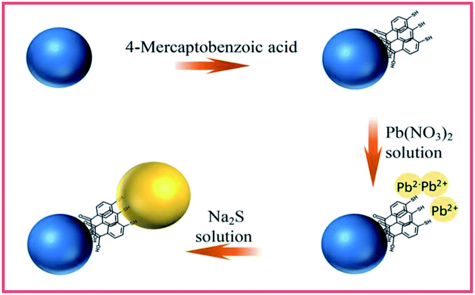 | ||
| Fig. 1 The fabrication process of TiO2/MBA/PbS system. | ||
Preparation of TiO2/MBA/CdS system
In order to preparing TiO2/MBA/CdS system, we take advantage of the electrostatic interactions between nanoparticles and ions as previously described in the literature with only slight modifications.25 A 2 mM Cd(Ac)2·2H2O ethanol solution was then added into the prepared TiO2/MBA system to allow Cd2+ ions to absorb on the TiO2 NP surfaces under stirring. To crystallize the CdS NPs onto the TiO2 NPs, 6 mM thiourea was slowly added dropwise into the solution under vigorous stirring. Thereafter, the pH was adjusted to 10 with 0.2 M NaOH solution. Then the reaction was kept for an additional 12 h at room temperature. The resulting composite particles were washed with distilled water. After drying, the TiO2/MBA/CdS system was obtained.Instrumentation
TEM images were taken using a Jeol JEM 2100F transmission electron microscope operating at 200 kV. The crystal structure of samples was determined by X-ray diffraction (XRD) using a Siemens D5005 X-ray powder diffractometer with a Cu Kα radiation source at 40 kV and 30 mA. The ultraviolet-visible (UV-vis) diffuse reflectance spectra (UV-vis DRS) were recorded on a Lambda UV-950 UV-vis spectrometer. Raman spectra were obtained using a Horiba-Jobin Yvon LabRAM ARAMIS system. The 633 nm radiation from a 20 mW air-cooled HeNe narrow bandwidth laser was used as an exciting source. Data was acquired with the 10 s accumulations for MBA molecules in the different systems at ambient temperature. Meanwhile, to avoid the photodegradation effect, all the samples were tested with at a low laser power of 0.27 mW (monitored by filter D1).Results and discussion
Characterization of morphology and crystal structure of different systems
Fig. 2a and b shows the TEM image and the X-ray diffraction (XRD) pattern of the TiO2 NPs after hydrothermal processing and calcination. It can be seen from Fig. 2a that the TiO2 NPs are all irregular sphere-like particles with a diameter of about 10 nm. According to JPCDS 21-1272, the observed lattice spacing of 0.351 nm in Fig. 2a corresponds to the (101) plane of anatase TiO2. Fig. 2b shows the XRD pattern of TiO2 NPs calcined at 450 °C. In general, the XRD peak at 2θ = 25.3° is identified as the characteristic diffraction peak of the anatase phase of TiO2.26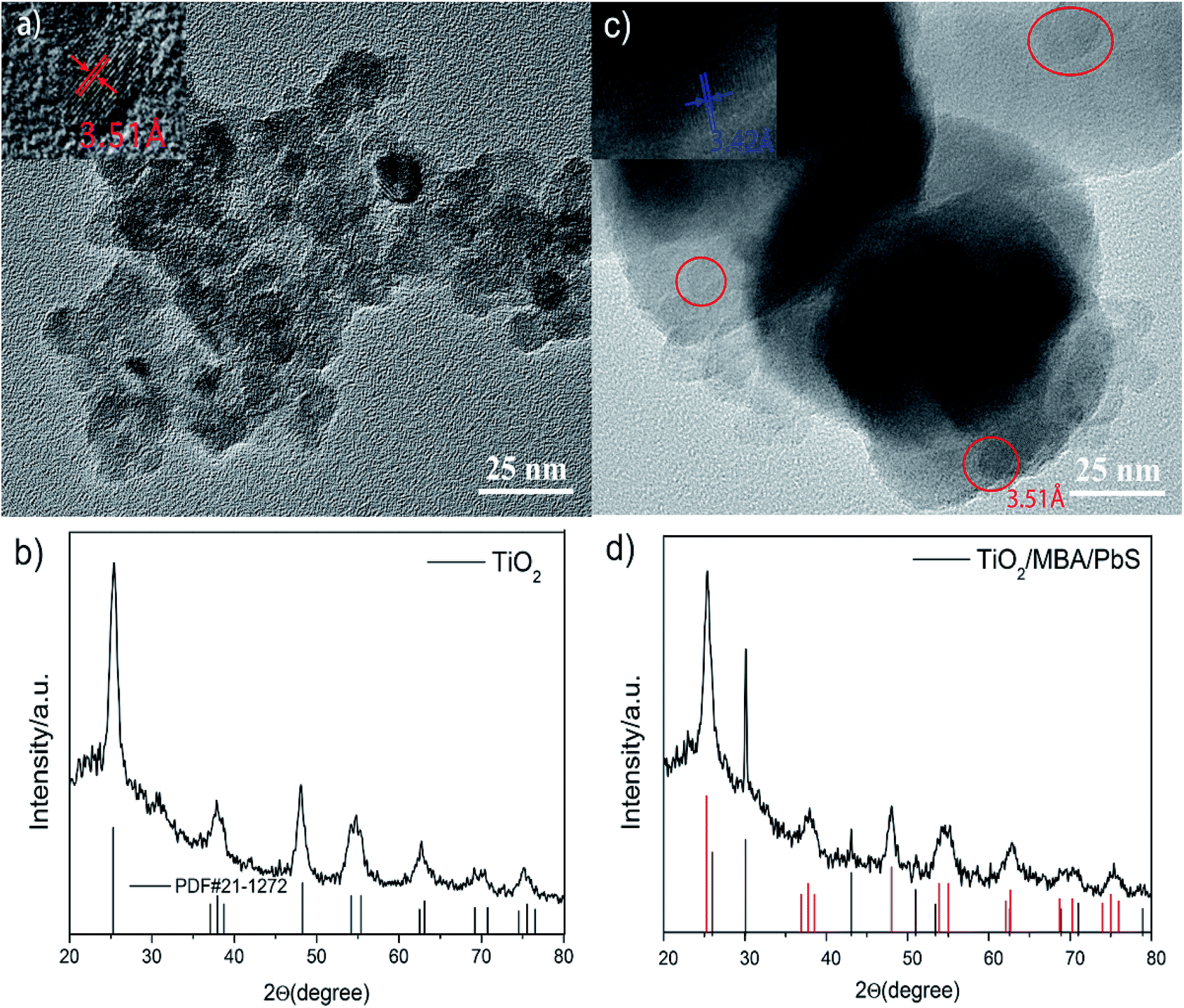 | ||
| Fig. 2 The TEM image and the XRD patterns of the pure TiO2 NPs (a and b) and TiO2/MBA/PbS system (c and d). In (c), the particles inside red circle are TiO2 NPs. | ||
Fig. 2b reveals that the TiO2 NPs calcined at 450 °C were monolithic anatase phase TiO2, which also agrees well with the reported data in JPCDS 21-1272. Estimated from the half-bandwidth (β) of the corresponding X-ray spectral peak by the Scherrer formula: D = kλ/(β![[thin space (1/6-em)]](https://www.rsc.org/images/entities/char_2009.gif) cosθ),27 the crystalline size D was about 9.1 nm, which is consistent with the size value obtained from the TEM image.
cosθ),27 the crystalline size D was about 9.1 nm, which is consistent with the size value obtained from the TEM image.
Fig. 2c and d presents the TEM image and the XRD patterns of the TiO2/MBA/PbS system. Inspection of the Fig. 2c TEM image reveals that PbS NPs, with an average diameter of about 70 nm, are surrounded by TiO2 NPs. The crystallinity of PbS NPs can clearly be seen, where the distance of the crystalline plane was measured to be 0.342 nm, indicating a (111) plane of cubic PbS (JPCDS 05-0592). Fig. 2d shows the XRD pattern of the TiO2/MBA/PbS system. The presence of PbS (black line, JPCD05-0592) and TiO2 (red line, JPCDS 21-1272) diffraction peaks can be observed clearly in Fig. 2d. Both the TEM image and the XRD pattern provide clear evidence of the successful fabrication of the TiO2/MBA/PbS system.
Measurement of UV-vis spectra
The UV-visible absorption spectra have obtained to characterize the photoelectric property of different systems. Fig. 3 shows the UV-vis absorption spectra of TiO2, TiO2/MBA and TiO2/MBA/PbS systems. Pure TiO2 shows a band-edge absorption around 395 nm (3.14 eV), which is close to the reported value.28 After modification by MBA molecules, the photoabsorption threshold of TiO2 exhibits a slight shift, which can be ascribed to the influence of the molecules adsorbed on TiO2 NPs. Similar phenomena have been observed in previous literatures.22,29,30 Moreover, its photoresponse is extended to about 600 nm. These changes can be attributed to a new charge-transfer (CT) complex formed between the adsorbed molecules and the TiO2 substrate. After introducing PbS NPs, the system shows a strong absorption of visible light because of PbS NPs presence. By comparison, we also synthesize cubic PbS NPs with similar diameter of about 70 nm (Fig. S1†). Fig. S2† shows the UV-vis absorption spectra of PbS NPs with strong absorption between 200–800 nm. Thus, it can be concluded that the TiO2/MBA/PbS coupled semiconductor nanoparticle system is fabricated.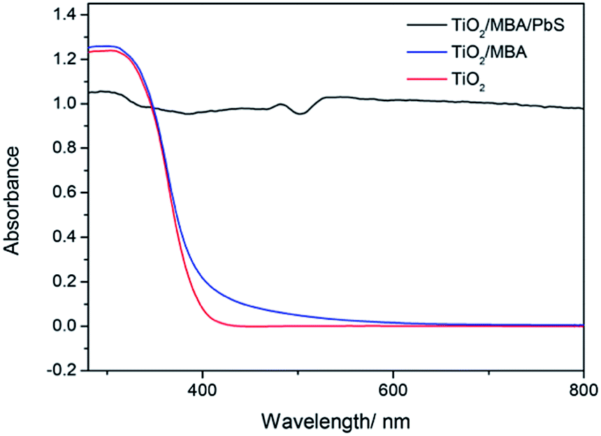 | ||
| Fig. 3 The UV-visible absorption spectra have obtained to characterize the photoelectric property of different systems. | ||
SERS spectra of different semiconductor systems
SERS spectra (excited at 633 nm) of MBA molecules in the TiO2/MBA and TiO2/MBA/PbS systems are shown in Fig. 4a.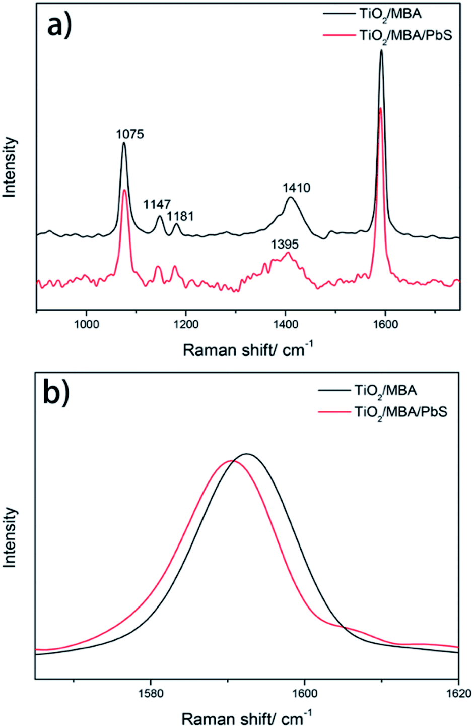 | ||
| Fig. 4 (a) The SERS spectra of TiO2/MBA and TiO2/MBA/PbS systems at 633 nm excitation and (b) the enlarged SERS spectra between 1565 and 1620 cm−1. | ||
To avoid the photodegradation effect of laser, all the samples were tested at a low laser power of 0.27 mW (monitored by filter D1).31 The Raman shifts and assignments of the bands are listed in Table 1.
| Wavenumbers (cm−1) | Band assignments |
|---|---|
| a ν, stretching; β, bending. For ring vibrations, the corresponding vibrational modes of benzene and the symmetry species with C2v symmetry are indicated. | |
| 1075 | In-plane ring breathing + ν(C–S) |
| 1147 | C–H deformation modes ν15, b2 |
| 1181 | C–H deformation modes ν9, a1 |
| 1411 | β(O–H) + ν(C-ph) + 19a + ν(CO2), b2 |
| 1583 | Non-totally symmetric ν(CC), b2 |
| 1592 | Totally symmetric ν(CC), a1 |
For MBA molecules in the TiO2/MBA system (black line, Fig. 4a), one of the predominant bands is located at 1075 cm−1, which has been assigned to the in-plane ring breathing mode coupled with ν(C–S). Another predominant band is an overlap result of two SERS bands: the aromatic ν(CC) mode (at 1592 cm−1) and the non-totally symmetric stretching mode (at 1583 cm−1).32,33 Two weak bands at about 1147 (ν15, b2) and 1181 cm−1 (ν9, a1) can also be observed and are attributed to the C–H deformation mode. These two weak bands are characteristic SERS signals of the 4-MBA molecule on the TiO2 substrates and consistent with those previously reported in TiO2/4-MBA systems. In previous works,30,34 the SERS signals in the TiO2/MBA system have been attributed to the dominant contribution of the TiO2-to-molecule CT mechanism. After introducing PbS NPs into the TiO2/MBA system (black line, Fig. 4a), some changes in the SERS bands were observed. For comparison, the Raman spectra were normalized using the band at 1075 cm−1. For clarity, the magnified SERS spectra of 4-MBA molecules between 1565 and 1620 cm−1 are shown in Fig. 4b. The band at 1583 cm−1 assigned to non-totally symmetric ν(CC) displays an increase in the intensity of the SERS spectrum after introducing PbS NPs, while band at 1592 cm−1 assigned to the aromatic ν(CC) mode has no distinct changes. Meanwhile, it is worth noting that the peak at 1410 cm−1 (Fig. 4a) is broadened and shifts after the introduction of PbS NPs, which provides more evidence that MBA molecules bind to TiO2 and PbS with COO− and –SH respectively (shown in ESI†). According to the previous report,35 the composite peak at 1411 cm−1, rising from the combination or overlap of O–H bending, the carboxyl carbon and aromatic carbon stretching, 19a (the Wilson notation) coupled with COO− asymmetric stretch, can be ascribed to b2 mode. Thus, due to the selective enhancement of b2 mode, the increased peak area at 1411 cm−1 is observed after the introduction of PbS NPs.
According to the CT model of Lombardi,21 only totally symmetric vibrational modes of the probe molecules are expected to be enhanced via the Franck–Condon contribution, and the Herzberg–Teller effect can enhance both totally and non-totally symmetric vibrational signatures in the SERS spectra of the probe molecules. That is, the b2 mode can be selectively enhanced by the CT mechanism through the Herzberg–Teller contribution. To further demonstrate the enhancement of b2 mode in the TiO2/MBA/PbS system, the nonlinear Lorentzian curve fit of the SERS spectra was performed. In Fig. 5a, an enhancement of the b2 mode in SERS spectra of MBA molecules is observed in the fit result. For comparison, we also calculated the intensity ratio between the two modes at 1583 cm−1 (b2) and 1075 cm−1 (a1) and plotted the column diagram (Fig. 5b). The band at 1075 cm−1 (C–S stretch, a1) was selected because it is intense and relatively isolated from interference. The fit result indicates that the b2 mode is enhanced selectively derived from the enhanced CT process that occurs after introducing PbS NPs into the TiO2/MBA system. As we know, the SERS signals in TiO2/MBA have been attributed to the dominant contribution of the TiO2-to-molecule CT mechanism.22,34,36 Then, it can be deduced that the introduction of PbS NPs enhances the TiO2-to-molecule CT process. These results agree with previous reports of the SERS spectra of MBA.33 Additionally, Fig. S3 in the ESI† shows the SERS spectrum of the PbS/MBA system, which further prove that the changes in SERS occur due to the interaction between TiO2 NPs and PbS NPs.
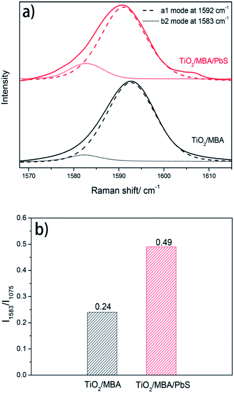 | ||
| Fig. 5 (a) The nonlinear Lorentzian fit curve of the SERS spectra in the TiO2/MBA and TiO2/MBA/PbS systems between 1568 and 1615 cm−1; (b) the SERS intensity ratio between the modes at 1583 and 1075 cm−1 spectra in the TiO2/MBA and TiO2/MBA/PbS systems. | ||
It is also noteworthy that the interaction in TiO2/MBA/PbS system also influences the phonon vibrational mode of TiO2 NPs. Fig. 6 shows the Raman spectra of TiO2 collected from TiO2/MBA and TiO2/MBA/PbS systems in the region of 100–700 cm−1. Raman modes at 145, 197, 398, 517 and 639 cm−1 are assigned as Eg, Eg, B1g, A1g (or B1g), and Eg modes in anatase phase, respectively.37 For comparison, they are also normalized to the intensity of the Eg(1) peak (145 cm−1 in TiO2/MBA). It can be observed that the peak at 145 cm−1 shifts toward higher wavenumbers and broadens after introducing PbS NPs into TiO2/MBA (Fig. 6b). As Fig. 4S† shows, the changes in TiO2/MBA/PbS come from the interaction between TiO2 and PbS, instead of MBA molecules. Thus, it can be deduced that the introduction of PbS NPs enhanced the CT process from TiO2 to MBA molecules, which further influences the phonon density of states in anatase TiO2. Then, the changes are reflected in the Raman spectra of TiO2 phonon vibrational mode. This phenomenon is similar to previous work where the light-induced transformations were observed due to the interaction between the TiO2 and Au NPs.38
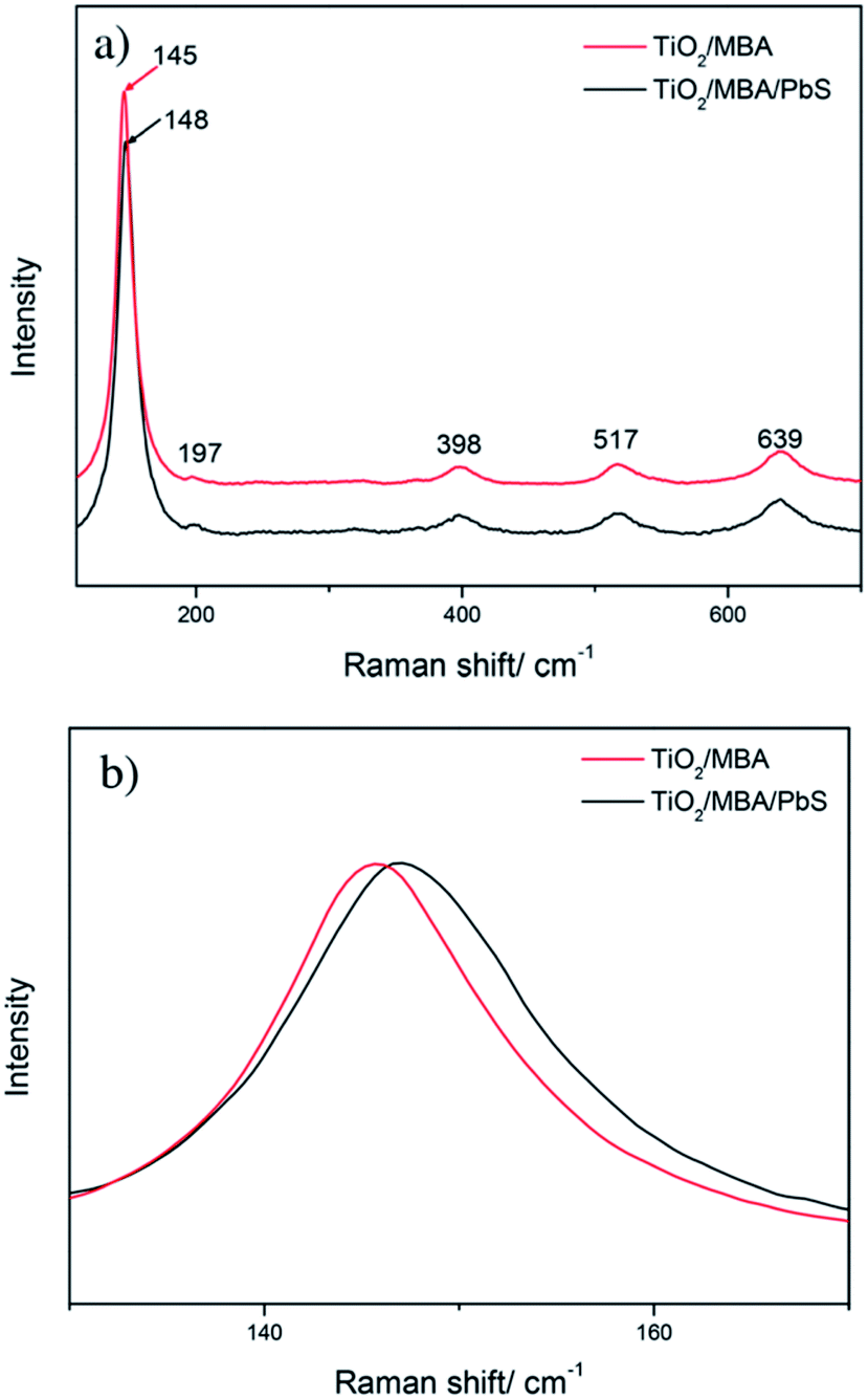 | ||
| Fig. 6 (a) The Raman spectra of TiO2 collected from TiO2/MBA and TiO2/MBA/PbS systems in the region of 100–700 cm−1 and (b) the enlarged SERS spectra between 130 and 170 cm−1. | ||
Analysis of the CT effect in the TiO2/MBA/PbS system
As Fig. 5 shows, the intensity of the SERS signal at 158 cm−1 (b2), driven by the enhancement of the TiO2-to-molecule CT process in TiO2/MBA/PbS system, is obviously higher than that in the TiO2/MBA system. According to previous work, in TiO2/MBA/Ag sandwich-structure system the stronger electrons attracting ability of Ag NPs promotes the TiO2-to-molecule CT process. In this work, it seems that the PbS NPs in TiO2/MBA/PbS system possibly play a similar role in the TiO2-to-molecule CT process. In previous work,23,39 efficient electron transfer from PbS QDs to TiO2 occurs only for QD diameters below approximately 4.3 nm. However, as Fig. 2c shows, the diameter of PbS NPs in our system is about 70 nm. And the work function of PbS NPs is 4.9 eV, which is higher than that of TiO2 NPs (4.7 eV).40,41 As the two kinds of materials with different work functions come in close contact with each other, the electrons are driven to transfer from one with lower work function to the other until equilibration of Fermi level. Therefore, when TiO2 NPs come into contact with PbS NPs in the TiO2/MBA/PbS system, electrons tend to transit from TiO2 to PbS, which is favorable to TiO2-to-molecule CT process. Then, the enhancement of b2-type vibrational mode is observed in SERS spectra (Fig. 5a). Similar phenomenon where the SERS spectra changes due to the interaction of two kinds of semiconductor NPs has been reported by Qian et al. previously.25 In their report, the SERS signal of bridge molecules show similar changes after introducing CdS NPs into the TiO2/MPA system. From the above discussion, it can be deduced that the interaction between the semiconductor NPs has an effect on the TiO2-to-molecule CT process. And the effect can be reflected in the SERS spectra where the CT-sensitive bands show enhancement under the interaction. Thus, the SERS model of the “donor–bridge–acceptor” system may be applicable to investigate the interfacial CT effect between different materials.SERS spectra of the TiO2/MBA/CdS system
To further confirm the proposed mechanism, we also investigated the SERS spectra of the TiO2/MBA/CdS system in Fig. 7. The XRD pattern and TEM of the TiO2/MBA/CdS system are shown in Fig. S5.† The work function of CdS NPs is 4.5 eV, which is lower than that of TiO2 NPs (4.7 eV).40,41 Therefore, when TiO2 NPs come in contact with CdS NPs in the TiO2/MBA/CdS system, electrons tend to transit from CdS NPs to TiO2, which is consistent with previous works. Then the TiO2-to-molecule CT process is inhibited. As we expect, the SERS spectra of the TiO2/MBA/CdS system would show opposite changes compared with the TiO2/MBA/PbS system. Fig. 7a shows the SERS spectra (excited at 633 nm) of MBA molecules in the TiO2/MBA and TiO2/MBA/CdS systems. For comparison, the Raman spectra were also normalized using the band at 1075 cm−1. After introducing CdS NPs, the band at 1583 cm−1 assigned to non-totally symmetric ν(CC) displays a decrease in the intensity of the SERS spectrum, while the band at 1592 cm−1 assigned to the aromatic ν(CC) mode shows no significate changes (Fig. 7c and d). The SERS spectrum of CdS/MBA is shown in Fig. S6† to exclude the interference from CdS/MBA.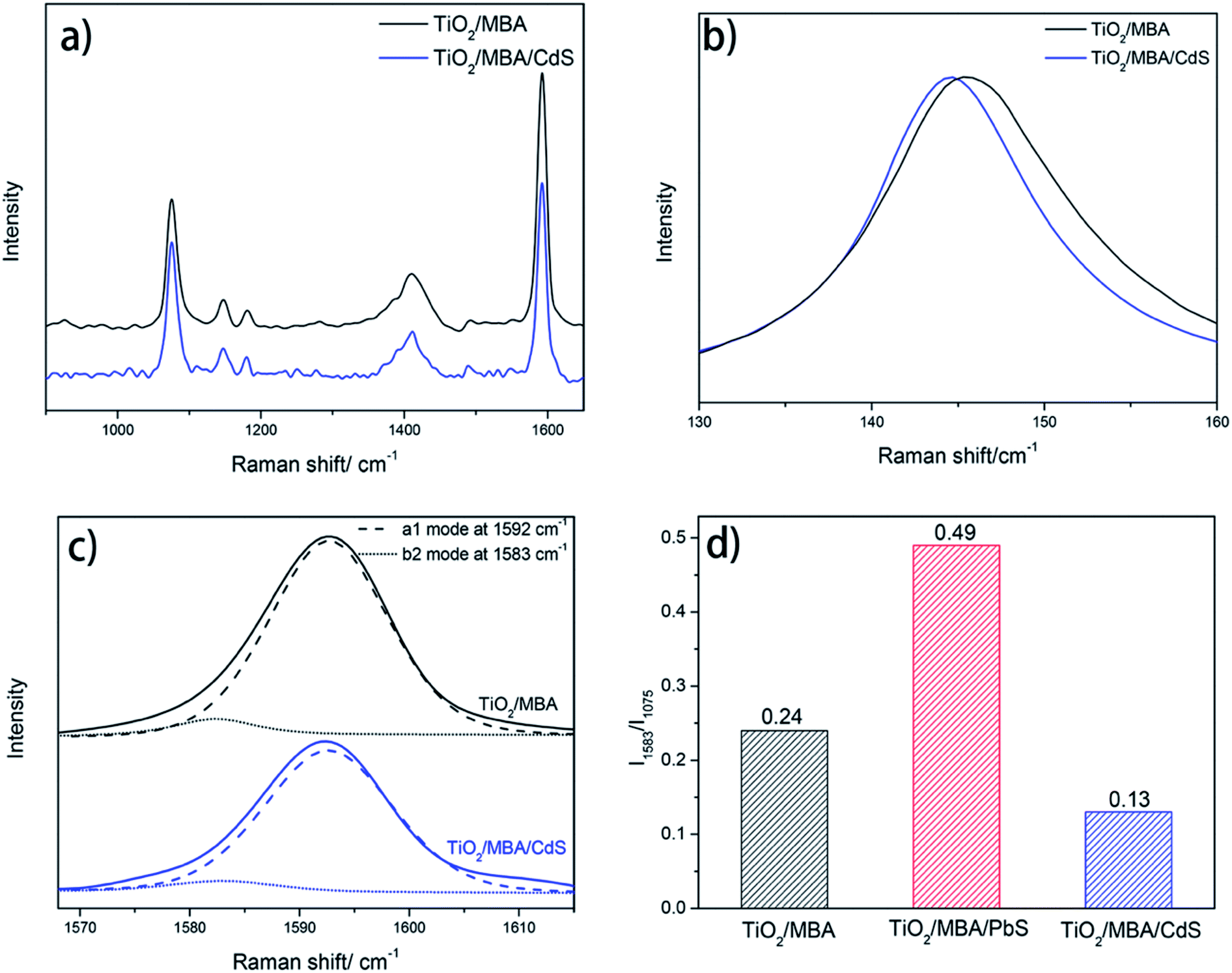 | ||
| Fig. 7 (a) The SERS spectra of the TiO2/MBA and TiO2/MBA/CdS systems at 633 excitation, and (b) the enlarged SERS spectra between 1560 and 1620 cm−1; (b) the enlarged SERS spectra between 130 and 170 cm−1; (c) the nonlinear Lorentzian curve fit of the SERS spectra in TiO2/MBA and TiO2/MBA/CdS systems between 1568 and 1615 cm−1, and (d) the SERS intensity ratio between the modes at 1583 and 1075 cm−1 in the TiO2/MBA, TiO2/MBA/PbS and TiO2/MBA/CdS systems. | ||
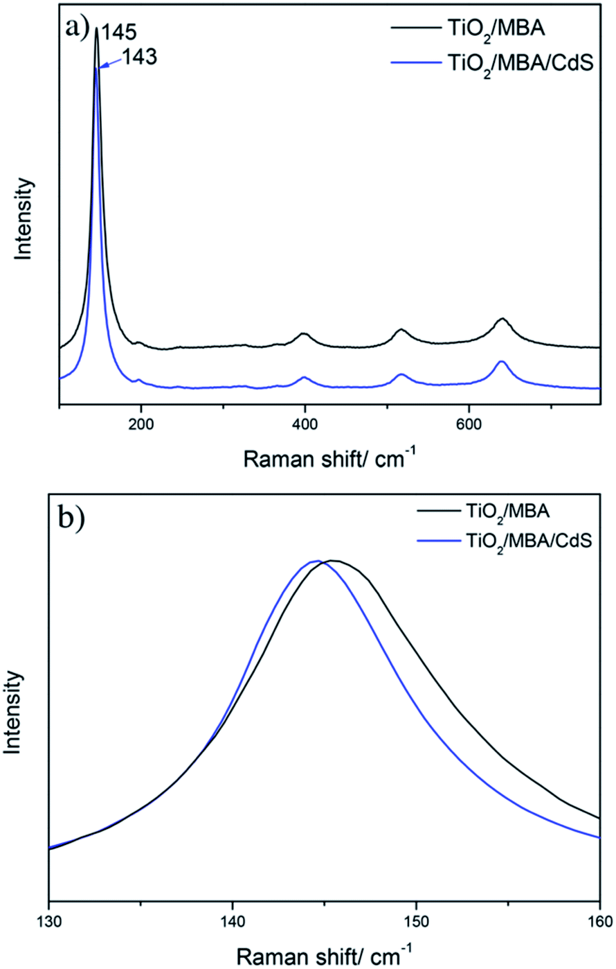
Meanwhile, the Raman spectra of TiO2 collected in the TiO2/MBA/CdS system also show opposite changes compared with the TiO2/MBA/PbS system. As Fig. 8 shows, the peak at 145 cm−1 shifts toward lower wavenumber and becomes narrower after introducing CdS NPs into TiO2/MBA, which is completely opposite to what we observed in the TiO2/MBA/PbS system.
 | ||
| Fig. 8 (a) The Raman spectra of TiO2 collected from the TiO2/MBA and TiO2/MBA/CdS systems, and (b) the enlarged SERS spectra between 130 and 160 cm−1. | ||
From above analysis, it can be deduced that the CT process between different semiconductor NPs has different effects on the TiO2-to-molecule CT process. And these effects on the TiO2-to-molecule CT process can be reflected in the SERS spectra where the CT-sensitive vibrational modes of probe molecules and the phonon vibrational mode of TiO2 show different changes. Thus, the CT process in coupled semiconductor nanoparticle systems can be investigated by applying the SERS method to a semiconductor-probe molecule-semiconductor physical model.
Conclusions
In this work, the TiO2/MBA/PbS system has been fabricated as a model to study the interfacial CT effects in coupled semiconductor nanoparticle system with SERS technique. As compared with the SERS signal in the TiO2/MBA system, the SERS signals of MBA in the TiO2/MBA/PbS system show distinct differences. The peak assigned to the b2 mode is significantly enhanced in the TiO2/MBA/PbS system. Meanwhile, the Raman spectra of TiO2 phonon vibrational mode also exhibit obvious difference in Raman frequency. These phenomena can be ascribed to the interaction between the TiO2 and PbS NPs where the CT trend from TiO2 to molecules is enhanced because the Fermi level of TiO2 is higher than that of PbS NPs. To prove this point, we also investigated SERS spectra of the TiO2/MBA/CdS system where the relative position of Fermi level is different from that of the TiO2/MBA/PbS system. And the result is in good accordance with our proposed mechanism. Thus, we can conclude from this work that it is possible to investigate the CT process in coupled semiconductor nanoparticle systems with a semiconductor–bridge molecule–semiconductor physical SERS model. It is expected that this study will not only provide a deep investigation of the CT process in coupled semiconductor nanoparticle systems but also be valuable for practical application of SERS technology in the nanomaterial field.Conflicts of interest
There are no conflicts to declare.Acknowledgements
The research was supported by the National Natural Science Foundation (Grants. 21273091, 21221063, 21327803, 21411140235, 21073072) of P. R. China; the 111 project (B06009); and the Development Program of the Science and Technology of Jilin Province (20110338, 20130305005GX).References
- Y. Bessekhouad, D. Robert and J. V. Weber, J. Photochem. Photobiol., A, 2004, 163, 569–580 CrossRef CAS.
- J. S. Im, S. K. Lee and Y.-S. Lee, Appl. Surf. Sci., 2011, 257, 2164–2169 CrossRef CAS.
- E. Ghadiri, B. Liu, J.-E. Moser, M. Grätzel and L. Etgar, Part. Part. Syst. Charact., 2015, 32, 483–488 CrossRef CAS.
- Z. He, W. Que, Y. Xing and X. Liu, J. Alloys Compd., 2016, 672, 481–488 CrossRef CAS.
- S. A. Mozaffari, M. Ranjbar, E. Kouhestanian, H. Salar Amoli and M. H. Armanmehr, Mater. Sci. Semicond. Process., 2015, 40, 285–292 CrossRef CAS.
- S. Sardar, P. Kar, S. Sarkar, P. Lemmens and S. K. Pal, Sol. Energy Mater. Sol. Cells, 2015, 134, 400–406 CrossRef CAS.
- M. Fleischmann, P. J. Hendra and A. J. McQuillan, Chem. Phys. Lett., 1974, 26, 163–166 CrossRef CAS.
- R. P. Li, J. L. Yang, J. H. Han, J. H. Liu and M. J. Huang, Phys. E, 2017, 88, 164–168 CrossRef CAS.
- C. Y. Zhang, R. Hao, B. Zhao, Y. Z. Fu, H. J. Zhang, S. Moeendarbari, C. S. Pickering, Y. W. Hao and Y. Q. Liu, Appl. Surf. Sci., 2017, 400, 49–56 CrossRef CAS.
- X. G. Zhang, Z. G. Dai, S. Y. Si, X. L. Zhang, W. Wu, H. B. Deng, F. B. Wang, X. H. Xiao and C. Z. Jiang, Small, 2017, 13, 1603347 CrossRef PubMed.
- R. Berenguer, A. La Rosa-Toro, C. Quijada and E. Morallon, Appl. Catal., B, 2017, 207, 286–296 CrossRef CAS.
- C. C. Lin, C. Y. Lin, C. J. Kao and C. H. Hung, Sens. Actuators, B, 2017, 241, 513–521 CrossRef CAS.
- K. K. Reza, J. Wang, R. Vaidyanathan, S. Dey, Y. L. Wang and M. Trau, Small, 2017, 13, 1602902 CrossRef PubMed.
- Y. Sun, L. Xu, F. D. Zhang, Z. G. Song, Y. W. Hu, Y. J. Ji, J. Y. Shen, B. Li, H. Z. Lu and H. F. Yang, Biosens. Bioelectron., 2017, 89, 906–912 CrossRef CAS PubMed.
- X. M. Li, M. H. Bi, L. Cui, Y. Z. Zhou, X. W. Du, S. Z. Qiao and J. Yang, Adv. Funct. Mater., 2017, 27, 1605703 CrossRef.
- A. K. Pal and D. B. Mohan, J. Alloys Compd., 2017, 698, 460–468 CrossRef CAS.
- S. G. Harroun, Y. T. Zhang, T. H. Chen, C. R. Ku and H. T. Chang, Spectrochim. Acta, Part A, 2017, 176, 1–7 CrossRef CAS PubMed.
- A. Campion and P. Kambhampati, Chem. Soc. Rev., 1998, 27, 241–250 RSC.
- R. S. Das and Y. K. Agrawal, Vib. Spectrosc., 2011, 57, 163–176 CrossRef CAS.
- E. J. Zeman and G. C. Schatz, J. Phys. Chem., 1987, 91, 634–643 CrossRef CAS.
- J. R. Lombardi and R. L. Birke, J. Phys. Chem. C, 2008, 112, 5605–5617 CAS.
- L. Yang, X. Jiang, W. Ruan, B. Zhao, W. Xu and J. R. Lombardi, J. Phys. Chem. C, 2008, 112, 20095–20098 CAS.
- C. Ratanatawanate, C. Xiong and K. J. Balkus, ACS Nano, 2008, 2, 1682–1688 CrossRef CAS PubMed.
- Y. Sun, E. Hao, X. Zhang, B. Yang, M. Gao and J. Shen, Chem. Commun., 1996, 2381–2382, 10.1039/CC9960002381.
- S. Qian, C. Wang, W. Liu, Y. Zhu, W. Yao and X. Lu, J. Mater. Chem., 2011, 21, 4945–4952 RSC.
- X. Xue, W. Ji, Z. Mao, Z. Li, W. Ruan, B. Zhao and J. R. Lombardi, Spectrochim. Acta, Part A, 2012, 95, 213–217 CrossRef CAS PubMed.
- W. Choi, A. Termin and M. R. Hoffmann, J. Phys. Chem., 1994, 98, 13669–13679 CrossRef.
- L. B. Liao, H. Y. Zhou and X. M. Xiao, Chem. Phys., 2005, 316, 164–170 CrossRef CAS.
- X. Xue, W. Ji, Z. Mao, H. Mao, Y. Wang, X. Wang, W. Ruan, B. Zhao and J. R. Lombardi, J. Phys. Chem. C, 2012, 116, 8792–8797 CAS.
- L. Yang, X. Jiang, W. Ruan, J. Yang, B. Zhao, W. Xu and J. R. Lombardi, J. Phys. Chem. C, 2009, 113, 16226–16231 CAS.
- P. Yin, R. U. I. Zhang, Y. Zhang and L. I. N. Guo, Int. J. Mod. Phys. B, 2010, 24, 3257–3262 CrossRef CAS.
- X. Zhang, Z. Yu, W. Ji, H. Sui, Q. Cong, X. Wang and B. Zhao, J. Phys. Chem. C, 2015, 119, 22439–22444 CAS.
- Y. Wang, W. Ji, H. Sui, Y. Kitahama, W. Ruan, Y. Ozaki and B. Zhao, J. Phys. Chem. C, 2014, 118, 10191–10197 CAS.
- X. Jiang, X. Li, X. Jia, G. Li, X. Wang, G. Wang, Z. Li, L. Yang and B. Zhao, J. Phys. Chem. C, 2012, 116, 14650–14655 CAS.
- R. Li, H. Lv, X. Zhang, P. Liu, L. Chen, J. Cheng and B. Zhao, Spectrochim. Acta, Part A, 2015, 148, 369–374 CrossRef CAS PubMed.
- L. Yang, Y. Zhang, W. Ruan, B. Zhao, W. Xu and J. R. Lombardi, J. Raman Spectrosc., 2009, 721–726, DOI:10.1002/jrs.2511.
- S. Kelly, F. H. Pollak and M. Tomkiewicz, J. Phys. Chem. B, 1997, 101, 2730–2734 CrossRef CAS.
- O. L. Stroyuk, V. M. Dzhagan, A. V. Kozytskiy, A. Y. Breslavskiy, S. Y. Kuchmiy, A. Villabona and D. R. T. Zahn, Mater. Sci. Semicond. Process., 2015, 37, 3–8 CrossRef CAS.
- D. F. Wang, H. G. Zhao, N. Q. Wu, M. A. El Khakani and D. L. Ma, J. Phys. Chem. Lett., 2010, 1, 1030–1035 CrossRef CAS.
- K. P. Bhandari, P. J. Roland, H. Mahabaduge, N. O. Haugen, C. R. Grice, S. Jeong, T. Dykstra, J. Gao and R. J. Ellingson, Sol. Energy Mater. Sol. Cells, 2013, 117, 476–482 CrossRef CAS.
- A. R. Kumarasinghe, W. R. Flavell, A. G. Thomas, A. K. Mallick, D. Tsoutsou, C. Chatwin, S. Rayner, P. Kirkham, S. Warren, S. Patel, P. Christian, P. O'Brien, M. Gratzel and R. Hengerer, J. Chem. Phys., 2007, 127, 114703 CrossRef CAS PubMed.
Footnote |
| † Electronic supplementary information (ESI) available. See DOI: 10.1039/c7ra07289a |
| This journal is © The Royal Society of Chemistry 2017 |