
 Open Access Article
 This Open Access Article is licensed under a
 Creative Commons Attribution 3.0 Unported Licence
Composites of epoxy/graphene-modified-diamond filler show enhanced thermal conductivity and high electrical insulation
Jin Jiang,
Feixiang Liu,
Kunyi Zhuang,
Danqing Chen* and
Guohua Chen *
*
School of Materials Science and Engineering, Huaqiao University, Xiamen 361021, China. E-mail: hdcgh@hqu.edu.cn; Fax: +86-592-6166296
First published on 22nd August 2017
Abstract
In this work, we developed a single-step process to cast epoxy composites having a high thermal conductivity but a low electric conductivity. Performance of the epoxy was improved by incorporating diamond microparticles that were covered with few-layer graphene sheets on surfaces. We found not only did this modified filler improve the dispersion of diamond in the polymer matrix but it also decreased the interfacial thermal resistance between the diamond and epoxy while preserving an excellent electrical insulation. Graphene on diamond particle surfaces was synthesized by a vacuum-based heating procedure. After 70 wt% of diamond fillers were added, we obtained a composite having a thermal conductivity of 2.85 W m−1 k−1, which is 101% better than that of the composite with 70 wt% pure diamond as the filler, and 1190% better than that of a neat epoxy, with electrical resistivity maintained at 2.2 × 10¹⁰ Ω m.
1. Introduction
Epoxy resins (EPs) have been widely applied in electrical insulators, printed circuit boards, and packaging materials as a matrix.1,2 Due to the rapid development in the microelectronics industry, electronic devices continue to move toward miniaturization, putting a large demand on rapid heat release from these small units.3 However, epoxy resins are poor heat conductors with a heat conduction coefficient of only 0.2–0.4 W m−1 k−1, which cannot meet the heat-dissipation requirements of modern electronics.4,5 A simple and common method is to introduce high thermal conductivity fillers into the matrix, including oxides (Al2O3, SiO2, ZnO),6–8 carbide (SiC),9 nitrides (AlN, BN, Si3N4)10,11 and carbon materials (graphene, graphite, diamond, carbon fiber).12–17 Among the diverse carbon materials, graphene attracts a great deal of attention owing to its fascinating physical properties. For example, graphene18 has been proposed as a promising heat transfer material due to its excellent in-plane thermal conductivity of 4100 ± 500 W m−1 k−1.19,20 Unfortunately, the addition of a small amount of graphene will also significantly increase the electrical conductivity of the polymer matrix, which is not desired for purposes of insulation in electronics packaging field. In order to solve this standing problem, oxides (SiO2,21,22 Al2O3,23,24 MgO25) and carbide (SiC26) were coated on the surface of graphene to prevent a direct contact of graphene flakes among each other. Subsequent preparation of composites, however, was found so complex that the loading level of the additives was fixed to a rather low level and hence not capable of substantially improve the thermal conductivity.Diamond on the other hand features an outstanding property in electrical insulation but with a high thermal conductivity reaching 2000 W m−1 k−1. Modifying diamond with monolayer graphene has been proposed as a prospect way to fabricate an excellent thermal conductor. In deed, several groups have attempted along this direction and, to name a few, Tzeng et al.27 synthesized graphene nanowalls on diamond nanoparticles by chemical vapor deposition (CVD) under a mixed gas stream of CH4 and H2; Garcia et al.28 grew multilayer graphene on diamond surfaces using a thin nickel film that was early deposited by e-beam evaporation.
Inspired by all these works, in this article, we demonstrate a novel epoxy composite that uses graphene-modified-diamond as the filler to improve thermal conductivity but without sacrificing electric insulation of the original resin. Our results show that the thermal conductivity in composites with 70 wt% diamond fillers was 2.85 W m−1 k−1, which is 101% better than that of the composites with 70 wt% pure diamond and 1190% better than that of the neat epoxy, with the electrical resistivity maintained at a high level of 2.2 × 10¹⁰ Ω m. We present the filler fabrication process and later composite characterizations in the rest of this article below.
2. Experimental section
2.1 Chemicals and materials
Epoxy resin (bisphenol A epoxy resin, E 6002) was provided by Shanghai Chemical Co., Ltd. The curing agent was diethyl methyl benzene diamine (DETDA; provided by Shanghai DE Alum Chemical Co., Ltd). Diamond was purchased from Hongyuan Diamond Technology Co., Ltd. Nickel powders were purchased from Aladdin Industrial Cooperation. Hydrochloric acid was purchased from Sinopharm Chemical Reagent Co., Ltd. Commercial graphene powders (G5) was purchased from Xia'men Kano Graphene Technology Co., Ltd. All these materials and chemicals were used as received without further purifications.2.2 Experimental processes
![[thin space (1/6-em)]](https://www.rsc.org/images/entities/char_2009.gif) :0, 99:1, 49:1, 19:1, 9:1, to 1:1. These mixtures were set in a silica crucible, and then put in a tube furnace that was pumped to a base pressure below 5 Pa. Later, these powders were heated up to 1273 K and kept at this temperature for 2 h. After cooling to room temperature, the powders were poured into a dilute hydrochloric acid solution and slowly stirred for several hours to get rid of the nickel elements. Finally, these modified diamond fillers were cleaned in distilled water several times to remove nickel chloride and hydrochloric acid before being kept inside a drying oven for later use.:0) 0.7/EP, D (99:1) 0.7/EP, D (49:1) 0.7/EP, D (19:1) 0.7/EP, D (9:1) 0.7/EP, where 0.7 represents the weight percent of the fillers to epoxy matrix, D (99:1) represents the surface modified diamond particles in the condition that the mass ratio between diamond and nickel is 99:1.
:0, 99:1, 49:1, 19:1, 9:1, to 1:1. These mixtures were set in a silica crucible, and then put in a tube furnace that was pumped to a base pressure below 5 Pa. Later, these powders were heated up to 1273 K and kept at this temperature for 2 h. After cooling to room temperature, the powders were poured into a dilute hydrochloric acid solution and slowly stirred for several hours to get rid of the nickel elements. Finally, these modified diamond fillers were cleaned in distilled water several times to remove nickel chloride and hydrochloric acid before being kept inside a drying oven for later use.:0) 0.7/EP, D (99:1) 0.7/EP, D (49:1) 0.7/EP, D (19:1) 0.7/EP, D (9:1) 0.7/EP, where 0.7 represents the weight percent of the fillers to epoxy matrix, D (99:1) represents the surface modified diamond particles in the condition that the mass ratio between diamond and nickel is 99:1.2.3 Characterizations
Samples were characterized by Scanning Electron Microscope (SEM), High-Resolution Transmission Electron Microscope (HRTEM), X-ray diffraction (XRD), Raman spectroscopy and X-ray photoelectron spectroscopy (XPS). SEM was taken on a JSM-6700F field-emitting scanning electron microscope with an operating voltage of 5 kV. High-resolution transmission electron microscope images were taken with JEM-2100 (HRTEM) to investigate the layers of the graphene sheets. X-ray diffraction (XRD) patterns were recorded with a D8-Advance Instrument (Bruker AXS) using Cu Kα radiation generated at a voltage of 40 kV and a current of 40 mA. The range of 2θ was from 10° to 70° with a scanning rate of 5° per minute. Raman spectra was recorded from 500 to 3500 cm−1 on a Raman spectrometer. XPS was carried out on a ThermoVG RSCAKAB 250X high-resolution X-ray photoelectron spectroscope. The thermal diffusivity (α) of the composites was measured by laser flash method using LFA447 (Nano-flash, NETZSCH, Germany). The thermal conductivity was calculated by K = α × ρ × Cp, in which Cp and ρ are the heat capacity and density of the composites, respectively. The Cp was measured using differential scanning calorimeter (DSC 200DSC). The volume resistivity (ρv) of the materials was collected using the AVO meter (UT70A) and measuring instrument for insulation resistance (ZC36). All the measurements were operated at room temperature.3. Results and discussion
3.1 Graphene microstructure and growth mechanism on diamond surface
Fig. 1a, c and e are SEM images of surface modified diamond microparticles. Different amount of graphene was deposited with loading ratio between diamond and nickel catalyst varied between 1:1, 9:1, and 49:1, respectively. Fig. 1b, d and f are enlarged views. When 1:1 ratio of diamond and nickel powders were mixed, most diamond surfaces are covered with graphene (Fig. 1a) that are smooth and folded (Fig. 1b). However, when diamond and nickel powders were mixed in other proportions, such as 9:1 and 49:1, the graphene can not uniformly distributed on the diamond surface anymore; with the decreasing in the number of nickel powders, the amount of graphene grown was less and less. Moreover, the graphene changed from a flake-like topography to spherical. Overall, the final amount of the graphene layers on diamond depends on the dosage of catalyst.
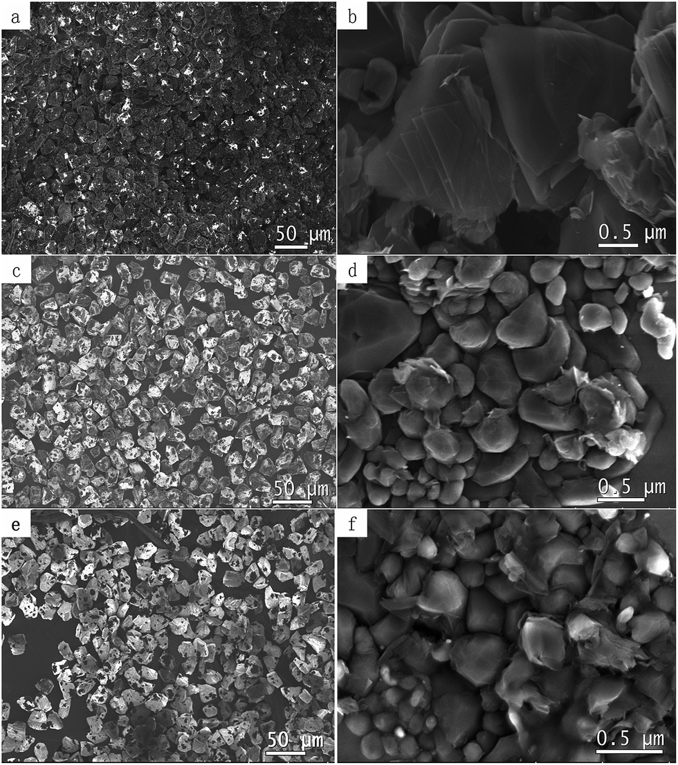 | ||
| Fig. 1 (a, c, e) SEM images of surface modified diamond microparticles with different coverage of graphene on surfaces, (b, d, f) SEM images of high magnification images. | ||
Fig. 2a and b demonstrate the morphology and thickness of graphene by TEM and high-resolution TEM images. Note these graphene flakes were intentionally removed from diamond particle surfaces with sonication, this diamond was treated with a very small amount of Ni (Ni/diamond = 1/49). Fig. 2a displays that the graphene sheet is flat. Another information on the thickness of these graphene sheets is provided by HRTEM in Fig. 2b, showing the number of graphene layers is approximately 3. The insert image in Fig. 2a is the corresponding selected area electron diffraction (SAED) pattern, which can further demonstrate the highly ordered crystalline structure of the graphene sheets.
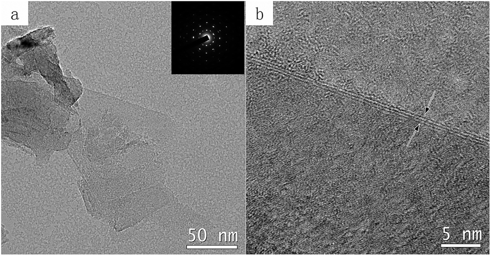 | ||
| Fig. 2 (a and b) TEM and HRTEM images of graphene on diamond microparticles surface. | ||
The XRD measurements in the 2θ range of 10–70° are shown in Fig. 3a, with a diffraction peak appearing at 44° in all the samples. This peak is a signature peak of highly crystalline diamond, which agrees with the observations described previously.30 After treatment with different proportions of nickel powders, the absence of another peak at around 26.4° confirms the formation of graphene. As illustrated in figure, with the reduction of graphene, the intensity of the peak gradually diminished.
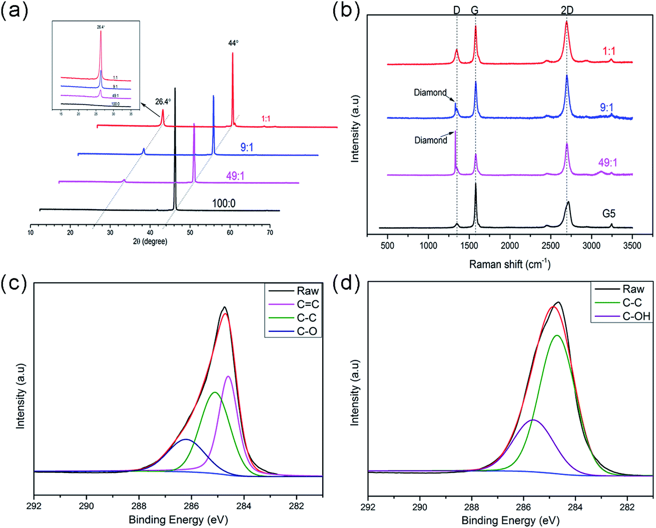 | ||
| Fig. 3 (a) X-ray diffraction patterns of graphene-modified-diamond under different conditions where the ratio between diamond and nickel catalyst is kept at 1:1, 9:1, 49:1, or 100:0; (b) Raman shift of commercial graphene (G5) and graphene-modified-diamond under different conditions where the ratio between diamond and nickel catalyst was kept at 1:1, 9:1, or 49:1; C1s XPS spectra of graphene-modified-diamond that was treated with a very small amount of Ni (Ni/diamond = 1/49) (c), pure diamond (d). | ||
Raman spectra of the graphene on diamond surfaces are shown in Fig. 3b. First, we see a sharp peak at 1332 cm−1, next to a satellite' peak of 1350 cm−1. The peaks at 1350 and 1580 cm−1 have been assigned as the typical D band and G band of graphene respectively.31–33 The D band is caused by the defect and disorder of graphene. The G band is generated from sp2 hybridized carbon bonds. Another 2D band near 2700 cm−1 is the characteristic peak of graphene structure, which can be used to estimate the number of layers of graphene. As revealed in Fig. 3b, the height of the 2D peak is about the same as the G peak when the diamond particles were treated on these conditions that the ratio between diamond and nickel particles were 1:1 and 9:1, this indicates that the graphene sheet is about 2–3 layers.
In addition, here we measure a single, sharp 2D peak in graphene, roughly 2 times more intense than the G peak when the ratio between diamond and nickel was 49:1. This indicates that the graphene sheet is 1–2 layers. The sharp peak at 1332 cm−1 is believed to be from the diamond. From all above, we conclude that the few-layer graphene has successfully grown on the surface of diamond. Furthermore, compared with commercial graphene, our samples have rather different 2D peak, where the 2D peak in commercial graphene consists of a relatively wide peak, roughly 1/2 the height of the G peak. Besides, when layers of graphene increase, a modest right shift happened. This shift referred by literature as a sign of thicker sheets of graphene.33
The XPS was employed to confirm the nature of the carbon and oxygen bonds appear in the graphene samples (Fig. 3c), the deconvoluted C1s XPS spectra of graphene-modified-diamond (Fig. 3c) showed three peaks corresponding to the carbon atoms in different functional groups, the peak at 284.5 eV corresponded to sp2 C![[double bond, length as m-dash]](https://www.rsc.org/images/entities/char_e001.gif) C hybridization, corresponding to graphitic carbon, the peak centered at around 285.0 eV corresponds to sp3 C–C hybridization. Another peaks at 286.2 eV is attributed to carbon bonding to oxygen (C–O), indicating some oxygen atoms chemically bond to the graphene that deposited on diamond surface.29 As revealed in Fig. 3d, the main peak centered at 284.8 eV is consistent with sp3 hybridization. The sp3 hybridization is considered to be derived from the diamond.
C hybridization, corresponding to graphitic carbon, the peak centered at around 285.0 eV corresponds to sp3 C–C hybridization. Another peaks at 286.2 eV is attributed to carbon bonding to oxygen (C–O), indicating some oxygen atoms chemically bond to the graphene that deposited on diamond surface.29 As revealed in Fig. 3d, the main peak centered at 284.8 eV is consistent with sp3 hybridization. The sp3 hybridization is considered to be derived from the diamond.
Fig. 4(1) is a schematic diagram of the fabrication process for the growth of graphene on the diamond surface. First, during heating process, carbon atoms from diamond can dissolve into the nickel particles. Second, upon cooling, these carbon atoms segregate to the surface of nickel particles, forming lager amount of multilayer and monolayer graphene. Last, the monolayer and multilayer graphene are formed on the diamond surface through the strong C–C σ bonds which were observed before in literatures.28,29,34
 | ||
| Fig. 4 Schematic diagram of diamond/epoxy composites. | ||
3.2 Thermal conductivity and electrically insulating performance of the epoxy composites
Good dispersion of the fillers in the polymer matrix is an important factor for achieving a desired performance. The dispersion of diamond in the epoxy matrix was characterized by SEM. Cross section images of the epoxy composites bulk are showed in Fig. 5, where Fig. 5a shows the dispersion of pristine diamond in the epoxy matrix and Fig. 5b and c are enlarged view of Fig. 5a. We notice that there were a certain degree of precipitation of diamond particles (Fig. 5c), probably due to a high density of diamond. Fig. 5d–h show the uniform dispersion of modified diamond with graphene in the epoxy matrix, probably due to the C–O bonds on the graphene surface. Therefore, a strong interfacial adhesion is formed because of the better interaction of the graphene-modified-diamond with the epoxy matrix.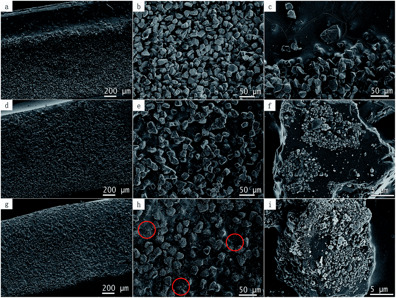 | ||
| Fig. 5 SEM micrographs of the epoxy composites loaded with 70 wt% of (a, b, c) pure diamond, (d, e, f) treated diamond with a low dosage of catalyst (catalyst/diamond = 1/49) and (g, h, i) treated diamond with a high dosage of catalyst (catalyst/diamond = 1/9). | ||
Fig. 5f and i are enlarged view of Fig. 5e and h, respectively. This diamond shown in Fig. 5f was treated with a very small amount of Ni (Ni/diamond = 1/49). We found the diamond surface was partially covered with spherical graphene. Interestingly, probably due to a strong carbon–carbon bond, graphene does not fall off easily; and the graphene growth did not seem to damage the diamond that much. Yet, the amount of graphene that grown on diamond surface was raised to a higher level when the loading ratio of catalyst is increased to 1/9. We see, some of the graphene can be stripped off and dispersed in epoxy resin, as shown in Fig. 5h and 4(2c). However, this was achieved with a serious damage from the catalyst erosion over diamond.
Both the thermal conductivity and thermal diffusivity of the epoxy composites are given in Fig. 6. When the diamond particles were pretreated with different dosage of catalyst, both terms changed with the amount of the nickel catalyst or the amount of graphenes. Specifically, the thermal conductivity (α) and thermal diffusivity (ĸ) increased first, then passed through a maximum, and later decreased at larger proportion of catalyst. It is worth noting that a high thermal diffusivity (1.12 mm2 s−1) was obtained with 70 wt% modified diamond (catalyst/diamond = 1/49)/epoxy composites as shown in Fig. 6. Corresponding thermal conductivity is 2.85 W m−1 k−1, which corresponds to a 101% increase compared to the value for the composite with 70 wt% pure diamond, and 1190% better than that of pure epoxy (pure epoxy resin had a thermal conductivity of 0.2 W m−1 k−1).35 Two aspects are explored to illustrate this relatively large improvement. First, thermal conductivity of graphene is intrinsically higher than diamond, the addition of graphene will minimize the interfacial thermal resistance with the epoxy resin. Second, we suspect a graphene decorated diamond disperses better probably due to the C–O bonds on the graphene surface. Therefore, a strong interfacial adhesion is formed between the filler and epoxy, making it easier to form a thermal pathway, as shown in Fig. 4 and 2b.
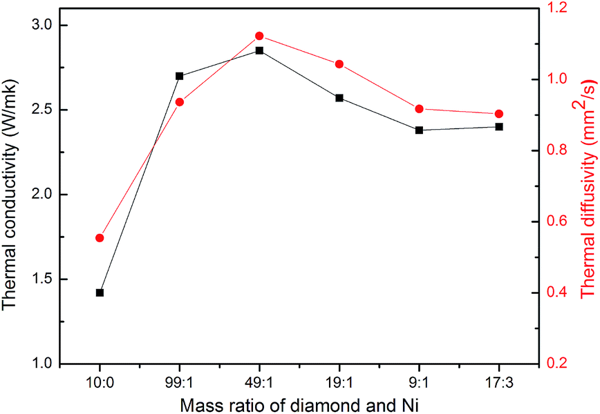 | ||
| Fig. 6 Thermal diffusivity (α) and thermal conductivity (ĸ) of 70 wt% diamond/epoxy composites varied with the amount of nickel catalyst during diamond surface treatment. | ||
However, both of these values decreased when diamond was mixed with a larger amount of catalyst. Since graphene was formed under the condition of catalyst erosion over the diamond, the destruction of diamond will be more severe at a high catalyst loading and this results in the deterioration of the thermal conductivity.
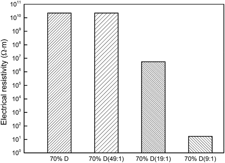
Fig. 7 shows the volumetric electrical resistivity of the epoxy/diamond composites, where a high value of 2.20 × 10¹⁰ Ω m was received for composites having 70 wt% pure diamond. Meanwhile, this value remained about the same for composites with 70 wt% modified diamond, as shown in Fig. 7. However, when the diamond was treated in the condition of a high catalyst loading of 1:9, the electrical resistivity declined sharply by 9 orders of magnitude and reached an extremely low value of 1.7 × 101 Ω m, which indicates that the electrical percolation network had already formed. Perhaps, some of the graphene has been stripped off, making it easier to form a conductive pathway, as marked by the red circle in the Fig. 5h.
 | ||
| Fig. 7 Volumetric electrical resistivity of the epoxy composites. | ||
4. Conclusions
In summary, the graphene-modified-diamond enhances contact area for thermal reinforcement in polymer matrix. After the pretreatment of diamond with a low dosage of catalyst (1/49), the thermal conductivity with 70 wt% fillers reached 2.85 W m−1 k−1, which corresponds to a 101% increase compared to the value of the composites with 70 wt% pure diamond, and 1190% better than that of pure epoxy. Moreover, the electrical insulation of the diamond powder effectively inhibited the electron transport. The prepared epoxy composites exhibited both outstanding thermal conductivity and electrical insulation, which could lead to enhanced application in the field of thermal management for electrical packaging.Conflicts of interest
There are no conflicts to declare.Acknowledgements
This work was financially supported by Natural Science Foundation of China (51373059), Science Foundation of Xia'men (3502Z20150046), science and technology innovation team of Huaqiao University (Z14X0046), and The Research Center of Graphene Powder & Composites of Fujian Province.Notes and references
- S. Rimdusit and H. Ishida, Polymer, 2000, 41, 7941–7949 CrossRef CAS.
- S. Zhao, L. S. Schadler, R. Duncan, H. Hillborg and T. Auletta, Compos. Sci. Technol., 2008, 68, 2965–2975 CrossRef CAS.
- H. Chen, V. V. Ginzburg, J. Yang, Y. Yang, W. Liu, Y. Huang, L. Du and B. Chen, Prog. Polym. Sci., 2016, 59, 41–85 CrossRef CAS.
- S. Ganguli, A. K. Roy and D. P. Anderson, Carbon, 2008, 46, 806–817 CrossRef CAS.
- M. J. Assael, K. D. Antoniadis and D. Tzetzis, Compos. Sci. Technol., 2008, 68, 3178–3183 CrossRef CAS.
- S. Choi and J. Kim, Composites, Part B, 2013, 51, 140–147 CrossRef CAS.
- Y. Heo, H. Im, J. Kim and J. Kim, J. Nanopart. Res., 2012, 14, 1–10 CrossRef.
- N. Chisholm, H. Mahfuz, V. K. Rangari, A. Ashfaq and S. Jeelani, Compos. Struct., 2005, 67, 115–124 CrossRef.
- T. L. Li and S. L. Hsu, J. Phys. Chem. B, 2010, 114, 6825–6829 CrossRef CAS PubMed.
- Z. Shi, M. Radwan, S. Kirihara, Y. Miyamoto and Z. Jin, Appl. Phys. Lett., 2009, 95, 224104 CrossRef.
- F. Yang, X. Zhao and P. Xiao, J. Eur. Ceram. Soc., 2010, 30, 3111–3116 CrossRef CAS.
- V. Goyal and A. A. Balandin, Appl. Phys. Lett., 2012, 100, 073113 CrossRef.
- K. Chu, W. Li, C. Jia and F. l. Tang, Appl. Phys. Lett., 2012, 101, 211903 CrossRef.
- Y. M. Chen and J. M. Ting, Carbon, 2002, 40, 359–362 CrossRef CAS.
- L. M. Veca, M. J. Meziani, W. Wang, X. Wang, F. Lu, P. Zhang, Y. Lin, R. Fee, J. W. Connell and Y. P. Sun, Adv. Mater., 2009, 21, 2088–2092 CrossRef CAS.
- S. Ganguli, A. K. Roy and D. P. Anderson, Carbon, 2008, 46, 806–817 CrossRef CAS.
- W. S. Lee and J. Yu, Diamond Relat. Mater., 2005, 14, 1647–1653 CrossRef CAS.
- K. S. Novoselov, A. K. Geim, S. V. Morozov, D. Jiang, Y. Zhang, S. V. Dubonos, I. V. Grigorieva and A. A. Firsov, science, 2004, 306, 666–669 CrossRef CAS PubMed.
- A. A. Balandin, S. Ghosh, W. Bao, I. Calizo, D. Teweldebrhan, F. Miao and C. N. Lau, Nano Lett., 2008, 8, 902–907 CrossRef CAS PubMed.
- S. Ghosh, W. Bao, D. L. Nika, S. Subrina, E. P. Pokatilov, C. N. Lau and A. A. Balandin, Nat. Mater., 2010, 9, 555–558 CrossRef CAS PubMed.
- X. Pu, H. B. Zhang, X. Li, C. Gui and Z. Z. Yu, RSC Adv., 2014, 4, 15297–15303 RSC.
- M. C. Hsiao, C. C. M. Ma, J. C. Chiang, K. K. Ho, T. Y. Chou, X. Xie, C. H. Tsai, L. H. Chang and C. K. Hsieh, Nanoscale, 2013, 5, 5863–5871 RSC.
- R. Sun, H. Yao, H. B. Zhang, Y. Li, Y. W. Mai and Z. Z. Yu, Compos. Sci. Technol., 2016, 137, 16–23 CrossRef CAS.
- R. Qian, J. Yu, C. Wu, X. Zhai and P. Jiang, RSC Adv., 2013, 3, 17373–17379 RSC.
- F. Du, W. Yang, F. Zhang, C. Y. Tang, S. Liu, L. Yin and W. C. Law, ACS Appl. Mater. Interfaces, 2015, 7, 14397–14403 CAS.
- Y. Wang, J. Yu, W. Dai, D. Wang, Y. Song, H. Bai, X. Zhou, C. Li, C. T. Lin and N. Jiang, RSC Adv., 2014, 4, 59409–59417 RSC.
- Y. Tzeng, W. L. Chen, C. Wu, J. Y. Lo and C. Y. Li, Carbon, 2013, 53, 120–129 CrossRef CAS.
- J. M. Garcia, R. He, M. P. Jiang, P. Kim, L. N. Pfeiffer and A. Pinczuk, Carbon, 2011, 49, 1006–1012 CrossRef CAS.
- H. H. Zou, H. Bai, J. H. Yu, Y. Wang, Q. L. Liao, K. Nishimura, L. M. Zeng and N. Jiang, Composites, Part B, 2015, 73, 57–60 CrossRef CAS.
- M. Pandey, R. D'Cunha and A. K. Tyagi, J. Alloys Compd., 2002, 333, 260–265 CrossRef CAS.
- S. Kurita, A. Yoshimura, H. Kawamoto, T. Uchida, K. Kojima, M. Tachibana, P. Molina-Morales and H. Nakai, J. Appl. Phys., 2005, 97, 104320 CrossRef.
- Z. Ni, H. Fan, Y. Feng, Z. Shen, B. Yang and Y. Wu, J. Chem. Phys., 2006, 124, 204703 CrossRef CAS PubMed.
- A. C. Ferrari, J. Meyer, V. Scardaci, C. Casiraghi, M. Lazzeri, F. Mauri, S. Piscanec, D. Jiang, K. Novoselov and S. Roth, Phys. Rev. Lett., 2006, 97, 187401 CrossRef CAS PubMed.
- Q. Yuan, H. Hu, J. Gao, F. Ding, Z. Liu and B. I. Yakobson, J. Am. Chem. Soc., 2011, 133, 16072–16079 CrossRef CAS PubMed.
- M. Donnay, S. Tzavalas and E. Logakis, Compos. Sci. Technol., 2015, 110, 152–158 CrossRef CAS.
| This journal is © The Royal Society of Chemistry 2017 |