
 Open Access Article
 This Open Access Article is licensed under a
 Creative Commons Attribution 3.0 Unported Licence
Narrowing the band gap to enhance the resistive switching properties of Pr3+-doped ZnO thin films by Cd-ion doping
Shuai He ,
Aize Hao,
Ni Qin and
Dinghua Bao*
,
Aize Hao,
Ni Qin and
Dinghua Bao*
State Key of Optoelectronic Materials and Technologies, School of Materials Science and Engineering, Sun Yat-Sen University, Guangzhou 510275, China. E-mail: stsbdh@mail.sysu.edu.cn; Fax: +86-20-84113273; Tel: +86-20-84113365
First published on 9th August 2017
Abstract
Pr3+/Cd2+ co-doped ZnO hexagonal structure thin films with c-axis preferred orientation were deposited on Pt/Ti/SiO2/Si substrates using a chemical solution deposition method, and the effect of Cd-ion doping on the resistive switching properties of Zn0.97−xPr0.03CdxO thin films (x = 0, 0.02, 0.04, and 0.06) has been investigated. The results showed that Cd-doping improved the resistive switching properties of the Pt/Zn0.97−xPr0.03CdxO/Pt devices. The resistive switching devices exhibited good endurance, long retention, and uniform switching voltages. The resistive switching characteristics also show a good temperature stability beneficial for further device applications. The I–V characteristics and their temperature dependence analysis indicated that the conduction mechanism was ohmic conduction behavior for the low resistance state and at low voltage region for the high resistance state, whereas the conduction mechanism at relatively higher voltage for the high resistance state is trap-controlled space charge limited current. The resistive switching process has been explained using a conductive filament-related formation/rupture mechanism considering the thermal effects and the migration of oxygen vacancies. The reasons for the improvement of resistive switching performance through Cd ion doping, were attributed to the decrease of the band gap and the control of oxygen vacancies.
1. Introduction
Resistive random access memory (RRAM) has been considered to be one of the promising candidates for next-generation nonvolatile memory.1–4 Generally, RRAM based on the resistive switching (RS) effect, is constructed in a metal/insulator/metal (MIM) sandwich formation, where the insulator is used as the storage medium sandwiched between two metal electrodes.5,6 After an electroforming process, the MIM memory cell exhibits reproducible switching properties between the high resistance state (HRS) and the low resistance state (LRS) which can be mainly classified into two types, the unipolar RS depending on electrical amplitude, and the bipolar RS depending on electrical polarity.7,8 Although the RS devices have many advantages, there are still several reliability issues to be overcome, such as high electroforming voltage, nonuniform distribution of the operating voltage and low device yield.9 To solve the above problems and improve the performance of devices, various approaches have been explored including impurity doping, nanoparticle incorporation, and interface engineering.10–12Binary oxides as most promising resistive memory material candidates have been widely investigated to understand the switching mechanisms.13–17 ZnO, a well-known oxide semiconductor, has also been studied with regard to its RS behavior and several excellent features, including large memory window, low processing temperature, and the possibility of fabricating transparent/flexible electronic devices.8–22 Compared with pure ZnO thin films,23–26 doped ZnO has been investigated to achieve improved device performance.27 Simanjuntak, et al. doped cobalt into ZnO resistive memory devices, compensating for the native defects, thus improving the RS performance.28 Yang and coworkers fabricated the Ag/ZnO:Mn/Pt device with a high HRS/LRS resistance ratio.29 The role of c-axis texture of ZnO thin films on ZnO based RRAMs has been studied by Pt/ZnO/Ru device.30 Our previous studies investigated the RS properties of Mg-doped ZnO and Pr-doped ZnO thin films.31,32 For the Mg-doped ZnO thin films, the resistance ratio of HRS and LRS shows an obvious increase due to the widened band gap. The good RS properties of Pt/Zn1−xPrxO/Pt memory devices have been achieved owing to effective control of oxygen vacancies by doping Pr ions. However, the effects of narrowing band gap on RS characteristics are unclear and further control of oxygen vacancies is worth investigating for improving the resistive switching performance and understanding the physical origin of resistive switching effect.
Considering that introduction of Cd ions into ZnO thin films would narrow the band gap and change the distribution of oxygen vacancies in the thin films,33,34 we prepared Cd-doped Zn0.97Pr0.03O thin films on fused silica substrates and Pt/Ti/SiO2/Si substrates. Our results indicated that the optical band gap shifted to the lower energy with increasing Cd ion doping content and the Pt/Zn0.97−xPr0.03CdxO/Pt devices showed stable and reversible RS properties at different temperatures. On the basis of the resistance-temperature dependence and analysis of current–voltage characteristics, the RS process has been explained using a conductive filament-related formation/rupture mechanism considering the thermal effects and the migration of oxygen vacancies.
2. Experimental procedure
Pr3+/Cd2+ co-doped wurtzite ZnO thin films were prepared on Pt/Ti/SiO2/Si substrates and fused silica substrates using a chemical solution deposition method. The precursor solutions were prepared according to nominal stoichiometry of Zn0.97−xPr0.03CdxO (ZPC), where x varied from 0 to 0.1, respectively, using zinc acetate dihydrate (Zn(CH3COO)2·2H2O), praseodymium nitrate pentahydrate (Pr(NO3)3·5H2O), and cadmium acetate dihydrate (Cd(CH3COO)2·2H2O) as starting materials and 2-methoxyethanol and diethanolamine as solvent and stabilizer, respectively. In brief, Zn(CH3COO)2·2H2O, Pr(NO3)3·5H2O, and Cd(CH3COO)2·2H2O were added to the mixture of 2-methoxyethanol and diethanolamine to form the precursor solutions (0.5 mol L−1) at 50 °C in air. After continuously stirring the mixed solution for 2 h, pellucid solutions were obtained. Before film deposition, Pt/Ti/SiO2/Si substrates were cleaned by ultrasonically treated in alcohol and acetone. A thin ZnO seed layer was firstly deposited on the Pt/Ti/SiO2/Si substrates and annealed at 700 °C for 5 min. The preparation method for the ZnO seed layer was reported in our previous study.31 Then, ZPC thin films were deposited by spin coating on the ZnO seed layer at 3000 rpm for 30 s and annealed in a tube furnace for 5 min at 700 °C. The spin coating and the annealing processes were repeated six times. After that, the deposited films were annealed at 700 °C for 1 h in air atmosphere. Finally, circular Pt top electrodes with a diameter of 300 μm were sputter-deposited on the surface of the thin films for electrical measurements.The crystal structure of the thin films was analyzed by an X-ray diffractometer (XRD, D/MAX 2200 VPC, Rigaku, Tokyo, Japan) with CuKα radiation operated at a working current of 26 mA and a working voltage of 40 kV. The surface and cross-sectional morphologies of the thin films were investigated by JSM-6330F field emission scanning electron microscopy (SEM). The optical transmission spectra of the films were measured using a UV-3150 UV/Visible spectrophotometer. The current–voltage (I–V) characteristics and retention performances of Pt/ZPC/Pt memory devices were measured at room temperature using a Keithley 236 sourcemeter. During the measurements in voltage sweep mode, the bias was defined as positive when the electrical current flowed from top electrode to bottom electrode.
3. Results and discussion
Fig. 1 shows the X-ray diffraction patterns of ZPC thin films on Pt/Ti/SiO2/Si substrates annealed at 700 °C. The diffraction peaks can be indexed according to JCPDS 36-1451 with a hexagonal phase. The magnified (002) peaks are shown in the right side of Fig. 1. With increasing Cd doping content, the strongest (002) peaks slightly shift to the low-angle sides, attributed to the lattice expansion because of the larger ionic radius of Cd2+ (0.95 Å) than that of Zn2+ (0.74 Å), suggesting that the Cd ion incorporated into the ZnO lattice, as is expected.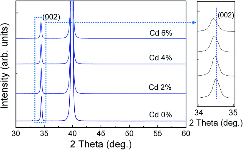 | ||
| Fig. 1 XRD pattern of Zn0.97−xPr0.03CdxO thin films annealed at 700 °C on Pt/Ti/SiO2/Si substrates. The right side of figure shows that the magnified (002) diffraction peak between 34° and 35°. | ||
The SEM surface and cross-sectional morphology images of the ZPC thin films prepared on Pt/Ti/SiO2/Si substrates annealed at 700 °C are shown in Fig. 2(a)–(d). The thin films exhibit crack-free and smooth surfaces, suggesting high packing density. The dense microstructure is beneficial for reliable electrical properties and uniform device quality. The cross-sectional SEM observation as shown in Fig. 2(e) indicates that the thickness of the thin film was approximately 180 nm for x = 0.04 sample. The other samples also have almost the same film thickness.
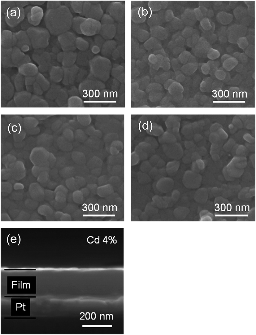 | ||
| Fig. 2 Surface morphology images of the Zn0.97−xPr0.03CdxO thin films with (a) x = 0, (b) x = 0.02, (c) x = 0.04, (d) x = 0.06, and (e) cross-sectional morphology image of the Zn0.93Pr0.03Cd0.04O thin film. The thin films were prepared on Pt/Ti/SiO2/Si substrates annealed at 700 °C. | ||
Fig. 3(a) shows the optical transmission spectra of ZPC films deposited on fused silica substrates with different Cd ion doping concentrations. All the thin films exhibit a high transmission in the visible region and a sharp ultraviolet absorption edge. The absorption edge has a red shift with increasing cadmium ion doping content (see the inset of Fig. 3(a)). The absorption coefficient (α) was calculated using Manifacier model.35 The dependence of α on the photon energy (hν) was fitted using the following equation:
| αhν = A(hν − Eg)n |
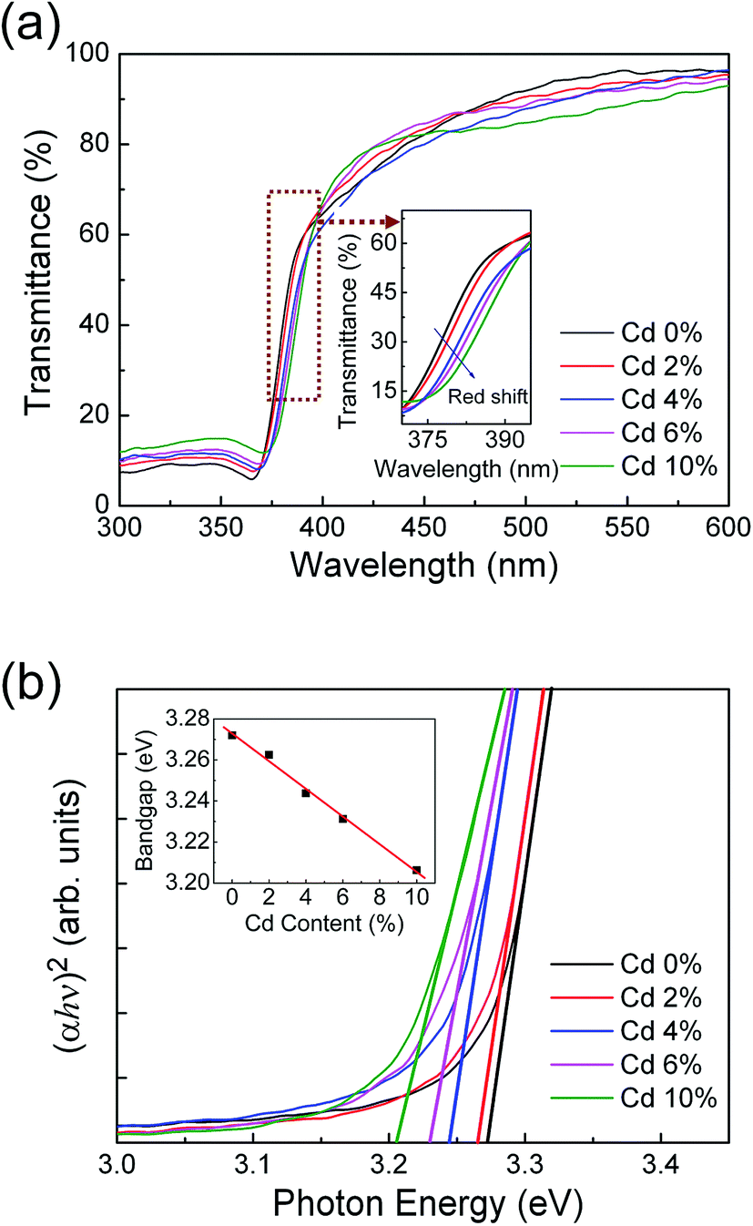 | ||
| Fig. 3 (a) Optical transmission spectra of the Zn0.97−xPr0.03CdxO thin films. The inset indicates a red shift of absorption edge as the Cd doping concentration increases. (b) Plot of (αhν)2 vs. photon energy for the Zn0.97−xPr0.03CdxO thin films. The inset indicates dependence of the optical band gap energies on Cd doping content. | ||
We investigated the effect of Cd ion doping content on RS properties of Zn0.97Pr0.03O thin films with Pt/ZPC/Pt configuration. Before characterizing the RS properties, an electroforming process is required to switch the memory cells from the initial HRS to LRS shown in insert of Fig. 4(a). Note that the electroforming voltage decreases from about 12 V to 9 V with increasing Cd content from 0% to 6%. After the electroforming process, these memory cells exhibited reproducible resistive switching properties as shown in Fig. 4(a). In addition, the reset and set processes can be carried out in the same voltage polarity regions of these memory cells, demonstrating that the RS properties depend on the voltage magnitude not the polarity of the voltage, shown in Fig. 4(b), and indicating a unipolar RS property. The Cd ion content dependence of the set voltage can also be clearly observed in Fig. 4(b). The critical value of set voltage decreases from 2.3 V to 1.6 V with increasing content of Cd ion from 0 to 6%. The decreasing set voltage is attributed to better conductivity due to Cd doping in the thin film, which is easier to soft breakdown. To avoid a dielectric hard breakdown, the compliance current (CC) is required, which is required to be larger than the current corresponding to the critical set voltage. There are small variations in the minimum CC for different devices. For pure and 2% Cd-doped film device, the CC should be larger than 5 and 8 mA, respectively, in which there is a stable unipolar RS property, whereas the 4% and 6% Cd-doped film devices exhibit the unipolar RS properties with Icc ≥ 10 mA.
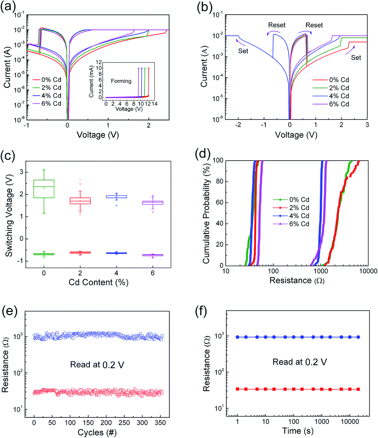 | ||
| Fig. 4 (a) Typical RS characteristic of the Pt/ZPC/Pt devices in semi-log scale. The inset exhibit the electroforming process of those devices. (b) RS behaviors of Pt/ZPC/Pt devices in the same voltage regions. (c) Distribution of set and reset voltages of Zn0.97−xPr0.03CdxO thin films. (d) Distribution of the programmed resistance of Zn0.97−xPr0.03CdxO thin films read at 0.2 V. (e) Endurance performance read at 0.2 V for the HRS (blue) and LRS (red). (f) Retention capability in Pt/Zn0.93Pr0.03Cd0.04O/Pt device. | ||
The distribution of the set and reset voltages of the ZPC thin films is shown in Fig. 4(c). The statistics of operating voltages indicates that the value of set voltage decreases obviously after doping Cd ions, and the distribution of set voltage exhibits a relatively more concentrated region for the Pt/Zn0.93Pr0.03Cd0.04O/Pt device. Fig. 4(d) presents the statistics of the programmed resistance of the memory cells, obtained by 100 successive I–V curves read at 0.2 V. It is noted that HRS/LRS resistance ratio of these memory cells is larger than 10, which meets requirement for memory applications. The coefficient of variation (σ/μ, where σ is the standard deviation and μ is the mean) of both resistance states were extracted from cumulative probability plot (shown in Table 1). The 4 mol% Cd-doped film device exhibits a tight distribution, with the σ/μ value of its LRS and HRS being 6.2% and 6.1%, respectively. In addition, steady resistive switching characteristics with 350 cycles with small fluctuations in the HRS and LRS were observed in the Pt/Zn0.93Pr0.03Cd0.04O/Pt device shown in Fig. 4(e). The retention capability of this device, obtained under the readout voltage of 0.2 V after switching the device to HRS or LRS, is illustrated in Fig. 4(f). The resistance values are stable without degradation, indicating that the device is nonvolatile.
| Coefficient of variation | ||
|---|---|---|
| HRS (%) | LRS (%) | |
| ZnO | 31.5 | 15.6 |
| 2% Cd | 46.4 | 4.3 |
| 4% Cd | 6.1 | 6.2 |
| 6% Cd | 15.4 | 15.4 |
In order to clarify underlying RS mechanism of the Pt/ZPC/Pt devices, the measured I–V curves are fitted with different conduction mechanisms, including Schottky emission, Poole–Frenkel, Fowler–Nordheim, and space charge limited current (SCLC) behavior. As shown in Fig. 5(a) and (b), it is found that ohmic conduction behavior dominates the LRS due to the linear relation of ln(I)–ln(V) with a slope of nearly 1. At the HRS, in the low voltage region (0–0.35 V), the I–V relationship shows a linear dependence on voltage, also corresponding to ohmic conduction region. When the applied voltage is larger than 0.35 V, the current increases rapidly with voltage, and follows square dependence on voltage, which agrees with the Child's square law (I–V2). The relation of ln(I)–ln(V) in the HRS also shows a very weak temperature dependence (see Fig. 6(a)). Therefore, the I–V features in the HRS can be well explained by space-charge-limited-current model.37–41 In summary, the conduction mechanism of LRS and low voltage region in HRS is ohmic conduction behavior, and the dominant conduction mechanism of HRS at relatively high voltage is space charge limited current behavior.
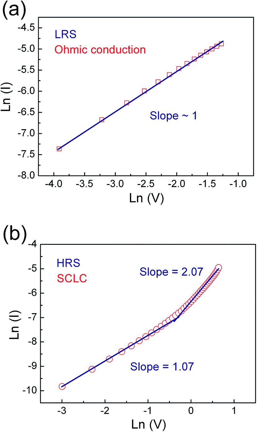 | ||
| Fig. 5 I–V curves plotted in double-log scale of Pt/Zn0.93Pr0.03Cd0.04O/Pt device in (a) LRS and (b) HRS. | ||
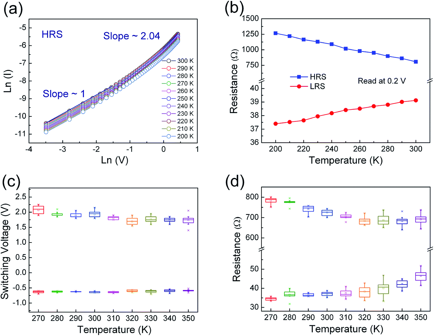 | ||
| Fig. 6 (a) I–V curves plotted in double-log scale of Zn0.93Pr0.03Cd0.04O thin film in HRS measured from 200 K to 300 K. (b) Resistance-temperature dependence of low and high resistance states read at 0.2 V. (c) Distribution of set and reset switching voltages of Pt/Zn0.93Pr0.03Cd0.04O/Pt device obtained by thirty continuous cycles at different temperature from 270 K to 350 K. (d) Statistics of programmed resistance of Pt/Zn0.93Pr0.03Cd0.04O/Pt device measured by the successive I–V curves read at 0.2 V from 270 K to 350 K. | ||
We have also investigated the temperature dependence of the resistance in low and high resistance states (shown in Fig. 6(b)). The resistance of the HRS increased linearly with decreasing temperature, indicating insulating or semiconducting behavior. In contrast, the resistance of the LRS increased with increasing temperature, indicating metallic conducting behavior. From a linear fit to the resistance of the LRS using the equation R(T) = R0[1 + α(T − T0)], the resistance temperature coefficient was determined to be α = 4.62 × 10⁻⁴ K−1, which is very close to that of oxygen-vacancy-based conductive filaments (5.8 × 10⁻⁴ K−1), and one order of magnitude lower than that Zn and Cd metals (about 4.2 × 10⁻³ K−1), suggesting that the conducting filaments mainly composed of oxygen vacancies formed in the resistive switching devices.42
Fig. 6(c) shows the distribution of set and reset switching voltages of Pt/Zn0.93Pr0.03Cd0.04O/Pt device obtained by thirty continuous cycles at different temperatures from 270 K to 350 K. It can be observed that the distribution of operating voltage was stably maintained up to 350 K. The corresponding device-to-device statistics of programmed resistance of Pt/Zn0.93Pr0.03Cd0.04O/Pt device measured by the successive I–V curves read at 0.2 V from 270 K to 350 K is shown in the Fig. 6(d). It is noteworthy that all of HRS/LRS resistance ratios are larger than 10 at different temperatures, and the resistance distribution at room temperature is more stable and uniform than that at higher temperature region which is attributed to thermal disturbance with regard to temperature. With increasing temperature, the average value of resistance of the HRS decreased, as shown in Fig. 6(d), until 320 K but began to be disturbed at 330 K. It is believed that a part of the conducting filaments that maintain the low conductivity in the HRS are destroyed by the heating effect and the sample decreases its electrical conductivity since 330 K.43
Based on the above results, the effects of Cd doping on the RS behavior of Zn0.97Pr0.03O thin films can be discussed as follows: firstly, low band gap and a lower HRS resistance and set/forming voltage for Cd-doped ZnO film have been confirmed. During the electroforming process, low band gap is beneficial to the transition of electrons from the valence band to the conduction band resulting in a lower forming voltage (see the inset of Fig. 4(a)). In addition, for HRS, filament has been ruptured in a local region.44 The conductivity in HRS depend on the remainder filament and nature of film material. For pure and Cd-doped ZnO films, the reset processes are similar (shown in Fig. 4(a) and (b)), implying the similar remainder filament for each device. However, the conductivity of film material is determined by the band gap of the material. Thus, Cd-doped film with narrowed band gap would show a greater conductivity, resulting in a low HRS resistance. Moreover, the worse insulativity makes it easy soft breakdown again, leading to lower set voltage (see Fig. 4(a) and (b)). Secondly, the distributions of the value of operating voltage and the resistance of HRS and LRS in the Cd2+ ion doped film devices are more stable and uniform than those of the undoped film device. The stability of RS characteristics is generally sensitive to the carrier concentration.43 It has been reported that in ZnO, the concentration of n-type carriers, mainly zinc interstitials and oxygen vacancies, increases with the increasing Cd ion doping content.45,46 First principles calculation by Tang, et al.47 also suggests that the formation energies of oxygen vacancies in Cd-doped ZnO are significantly lower than those in pure ZnO. In addition, the decreasing forming voltage and increasing leakage current with increasing Cd doping content, shown in the inset of Fig. 4(a), also act as an indirect evidence for increasing of defects. Hence, the Cd ion doping can be considered to equivalently increase the oxygen vacancies. The existence of more oxygen vacancies makes it easier to form the conducting filaments under driving voltage and to build more stable conducting filaments.48 In addition, since the ionic radius of Cd2+ ion is larger than that of Zn2+ ion, Cd2+ doping ion is easy to replace Zn2+ ion near the grain boundaries,49,50 whereas oxygen vacancies tend to accumulate in the grain boundaries. Thus, the Cd2+ ions can serve as chemical anchors for oxygen vacancies and confine the filament.51 As a result, more stable conducting filaments composed of oxygen vacancies can form along with the grain boundaries, which improve the stability and uniformity of RS properties.
Generally, a model involving the formation and rupture of filaments can be employed to explain the resistive switching phenomenon. Fig. 7 gives a simple description of the resistive switching process in our thin films. In the initial state, oxygen vacancies randomly distributed in the thin films, as shown in Fig. 7(a). After an electroforming process, lots of defects like oxygen vacancies and zinc interstitials have been produced, then gather together, and, finally, form conducting channels.52–54 The c-axis oriented grains confine conduction channels to extend along the grain boundaries, and go across the resistive switching layer, thus, the conduction channels connect the top and bottom electrodes, the conducting filaments are built up. As a result, the memory device was transited to LRS, as shown in Fig. 7(b). The electrons pass through the oxygen-vacancies bridge,55 exhibiting ohmic conduction behavior and holding on to the LRS until the conductive filaments are ruptured by thermal effect.7 Then, the device switches to HRS, as shown in Fig. 7(c). In HRS, the carriers are transported inside the film “bulk” by the trap controlled SCLC mechanism. At a lower voltage region, there are more thermally generated carriers than injected carriers from the electrode, and the I–V relationship shows a linear dependence on voltage, also corresponding to ohmic conduction behavior. With increasing applied voltage, the injected carriers are dominant which are captured by traps inside the film “bulk” and the current increases rapidly with voltage, resulting in trap controlled SCLC.38,42 Finally, the electron concentration in the thin films increases with increasing voltage, and the sample reaches the LRS again.
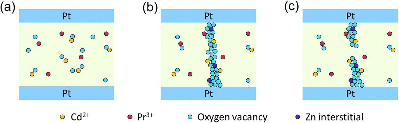 | ||
| Fig. 7 Schematic diagrams of (a) initial state, (b) low resistance state, and (c) high resistance state in Pt/Zn0.97−xPr0.03CdxO/Pt device. | ||
4. Conclusions
We have fabricated Zn0.97−xPr0.03CdxO thin films on fused silica substrates and Pt/Ti/SiO2/Si substrates by a chemical solution deposition method. The direct optical band gap shifted to the lower energy as a consequence of increasing Cd ion doping content in the thin films. The reversible and steady unipolar RS performances including uniform switching voltages, and long retention properties have been demonstrated in the Pt/Zn0.97−xPr0.03CdxO/Pt devices. The RS characteristics measured at different temperatures show a good stability which is beneficial for further device application. The improvement of RS performance with doping Cd ions is attributed to the decrease of band gap and the control of oxygen vacancies. The analysis of I–V characteristics and temperature dependence of resistance at HRS and LRS indicated that the conduction mechanisms were ohmic conduction in LRS and low voltage region in HRS, and trap-controlled SCLC in HRS at relatively high voltage, respectively. The resistive switching mechanism can be well explained by the formation and rupture of filaments composed of oxygen vacancies.Acknowledgements
The authors gratefully acknowledge financial support from Natural Science Foundation of China (No. 51372281) and Natural Science Foundation of Guangdong Province, China (No. 2015A030311019).References
- R. Waser, R. Dittmann, G. Staikov and K. Szot, Adv. Mater., 2009, 21, 2632–2663 CrossRef CAS.
- R. Waser and M. Aono, Nat. Mater., 2007, 6, 833–840 CrossRef CAS PubMed.
- J. J. S. Yang, D. B. Strukov and D. R. Stewart, Nat. Nanotechnol., 2013, 8, 13–24 CrossRef CAS PubMed.
- H.-S. P. Wong, H. Y. Lee, S. M. Yu, Y. S. Chen, Y. Wu, P. S. Chen, B. Lee, F. T. Chen and M. J. Tsai, Proc. IEEE, 2012, 100, 1951–1970 CrossRef CAS.
- K. M. Kim, D. S. Jeong and C. S. Hwang, Nanotechnology, 2011, 22, 25 Search PubMed.
- J. Choi, S. Park, J. Lee, K. Hong, D. H. Kim, C. W. Moon, G. D. Park, J. Suh, J. Hwang, S. Y. Kim, H. S. Jung, N. G. Park, S. Han, K. T. Nam and H. W. Jang, Adv. Mater., 2016, 28, 6562–6567 CrossRef CAS PubMed.
- D. B. Strukov, G. S. Snider, D. R. Stewart and R. S. Williams, Nature, 2008, 453, 80–83 CrossRef CAS PubMed.
- W. Hu, N. Qin, G. H. Wu, Y. T. Lin, S. W. Li and D. H. Bao, J. Am. Chem. Soc., 2012, 134, 14658–14661 CrossRef CAS PubMed.
- M. J. Lee, C. B. Lee, D. Lee, S. R. Lee, M. Chang, J. H. Hur, Y. B. Kim, C. J. Kim, D. H. Seo, S. Seo, U. I. Chung, I. K. Yoo and K. Kim, Nat. Mater., 2011, 10, 625–630 CrossRef CAS PubMed.
- K. Jung, J. Choi, Y. Kim, H. Im, S. Seo, R. Jung, D. Kim, J. S. Kim, B. H. Park and J. P. Hong, J. Appl. Phys., 2008, 103, 034504 CrossRef.
- L. Shi, D. S. Shang, Y. S. Chen, J. Wang, J. R. Sun and B. G. Shen, J. Phys. D: Appl. Phys., 2011, 44, 455305 CrossRef.
- F. M. Simanjuntak, D. Panda, T. L. Tsai, C. A. Lin, K. H. Wei and T. Y. Tseng, Enhanced switching uniformity in AZO/ZnO1−x/ITO transparent resistive memory devices by bipolar double forming, Appl. Phys. Lett., 2015, 107, 033505 CrossRef.
- S. Seo, M. J. Lee, D. H. Seo, E. J. Jeoung, D.-S. Suh, Y. S. Joung, I. K. Yoo, I. R. Hwang, S. H. Kim, I. S. Byun, J.-S. Kim, J. S. Choi and B. H. Park, Appl. Phys. Lett., 2004, 85, 5655–5657 CrossRef CAS.
- D. Panda, C. Y. Huang and T. Y. Tseng, Appl. Phys. Lett., 2012, 100, 112901 CrossRef.
- W. H. Guan, M. Liu, S. B. Long, Q. Liu and W. Wang, Appl. Phys. Lett., 2008, 93, 223506 CrossRef.
- D. Panda and T. Y. Tseng, Thin Solid Films, 2013, 531, 1–20 CrossRef CAS.
- D. Panda, A. Dhar and S. K. Ray, IEEE Trans. Nanotechnol., 2012, 11, 51 CrossRef.
- W. Y. Chang, Y. C. Lai, T. B. Wu, S. F. Wang, F. Chen and M. J. Tsai, Appl. Phys. Lett., 2008, 92, 022110 CrossRef.
- H. Y. Peng, G. P. Li, J. Y. Ye, Z. P. Wei, Z. Zhang, D. D. Wang, G. Z. Xing and T. Wu, Appl. Phys. Lett., 2010, 96, 192113 CrossRef.
- S. T. Han, Y. Zhou and V. A. L. Roy, Adv. Mater., 2013, 25, 5425–5449 CrossRef CAS PubMed.
- F. Zhuge, S. Peng, C. He, X. Zhu, X. Chen, Y. Liu and R. W. Li, Nanotechnology, 2011, 22, 275204 CrossRef PubMed.
- D. Panda and T. Y. Tseng, J. Mater. Sci., 2013, 48, 6849–6877 CrossRef CAS.
- W. H. Xue, W. Xiao, J. Shang, X. X. Chen, X. J. Zhu, L. Pan, H. W. Tan, W. B. Zhang, Z. H. Ji, G. Liu, X. H. Xu, J. Ding and R. W. Li, Nanotechnology, 2014, 25, 425204 CrossRef CAS PubMed.
- Y. C. Yang, X. X. Zhang, M. Gao, F. Zeng, W. Y. Zhou, S. S. Xie and F. Pan, Nanoscale, 2011, 3, 1917–1921 RSC.
- J. Qi, M. Olmedo, J. J. Ren, N. Zhan, J. Z. Zhao, J. G. Zheng and J. L. Liu, ACS Nano, 2012, 6, 1051–1058 CrossRef CAS PubMed.
- F. M. Simanjuntak, D. Panda, T. L. Tsai, C. A. Lin, K. H. Wei and T. Y. Tseng, J. Mater. Sci., 2015, 50, 6961–6969 CrossRef CAS.
- F. M. Simanjuntak, D. Panda, K. H. Wei and T. Y. Tseng, Nanoscale Res. Lett., 2016, 11, 368 CrossRef PubMed.
- F. M. Simanjuntak, O. K. Prasad, D. Panda, C. A. Lin, T. L. Tsai, K. H. Wei and T. Y. Tseng, Appl. Phys. Lett., 2016, 108, 183506 CrossRef.
- Y. C. Yang, F. Pan, Q. Liu, M. Liu and F. Zeng, Nano Lett., 2009, 9, 1636–1643 CrossRef CAS PubMed.
- Z. J. Liu, J. C. Chou, S. Y. Wei, J. Y. Gan and T. R. Yew, IEEE Electron Device Lett., 2011, 32, 1728–1730 CrossRef CAS.
- X. M. Chen, G. H. Wu and D. H. Bao, Appl. Phys. Lett., 2008, 93, 093501 CrossRef.
- S. He, A. Z. Hao, N. Qin and D. H. Bao, Ceram. Int., 2017 DOI:10.1016/j.ceramint.2017.05.213.
- T. Makino, Y. Segawa, M. Kawasaki, A. Ohtomo, R. Shiroki, K. Tamura, T. Yasuda and H. Koinuma, Appl. Phys. Lett., 2001, 78, 1237–1239 CrossRef CAS.
- S. Vijayalakshmi, S. Venkataraj and R. Jayavel, J. Phys. D: Appl. Phys., 2008, 41, 245403 CrossRef.
- J. C. Manifacier, M. D. Murcia, J. P. Fillard and E. Vicario, Thin Solid Films, 1977, 41, 127–135 CrossRef CAS.
- R. Maity and K. K. Chattopadhyay, Sol. Energy Mater. Sol. Cells, 2006, 90, 597–606 CrossRef CAS.
- Y. D. Xia, W. Y. He, L. Chen, X. K. Meng and Z. G. Liu, Appl. Phys. Lett., 2007, 90, 022907 CrossRef.
- Q. Liu, W. H. Guan, S. B. Long, R. Jia, M. Liu and J. N. Chen, Appl. Phys. Lett., 2008, 92, 012117 CrossRef.
- W. Hu, L. L. Zou, X. M. Chen, N. Qin, S. W. Li and D. H. Bao, ACS Appl. Mater. Interfaces, 2014, 6, 5012–5017 CAS.
- K. M. Kim, B. J. Choi, M. H. Lee, G. H. Kim, S. J. Song, J. Y. Seok, J. H. Yoon, S. Han and C. S. Hwang, J. Nanotechnol., 2011, 22, 254010 CrossRef PubMed.
- W. Y. Chang, Y. C. Lai, T. B. Wu, S. F. Wang, F. Chen and M. J. Tsai, Appl. Phys. Lett., 2008, 92, 022110 CrossRef.
- Z. Q. Wang, H. Y. Xu, X. H. Li, X. T. Zhang, Y. X. Liu and Y. C. Liu, IEEE Electron Device Lett., 2011, 32, 1442–1444 CrossRef CAS.
- N. Xu, L. F. Liu, X. Sun, X. y. Liu, D. D. Han, Y. Wang, R. Q. Han, J. F. Kang and B. Yu, Appl. Phys. Lett., 2008, 92, 232112 CrossRef.
- D. Panda and T. Y. Tseng, Ferroelectrics, 2014, 471, 23–64 CrossRef CAS.
- C. W. Sun, P. Xin, C. Y. Ma, Z. W. Liu and Q. Y. Zhang, Appl. Phys. Lett., 2006, 89, 1923 Search PubMed.
- A. D. Acharya, S. Moghe, R. Panda, S. B. Shrivastava, M. Gangrade, T. Shripathi, D. M. Phase and V. Ganesan, Thin Solid Films, 2012, 525, 49–55 CrossRef CAS.
- X. Tang, H. F. Lü, Q. Y. Zhang, J. J. Zhao and Y. Y. Lin, Solid State Sci., 2011, 13, 384–387 CrossRef CAS.
- H. T. Xu, D. H. Kim, X. H. Zhao, Y. Li, M. Y. Zhu, B. Lee and C. L. Liu, J. Alloys Compd., 2016, 658, 806–812 CrossRef CAS.
- C. Park, S. H. Jeon, S. C. Chae, S. Han, B. H. Park, S. Seo and D. W. Kim, Appl. Phys. Lett., 2008, 93, 042102 CrossRef.
- J. Zhang, X. Z. Li, J. Shi, Y. F. Lu and D. J. Sellmyer, J. Phys.: Condens. Matter, 2010, 22, 276002 CrossRef PubMed.
- K. A. Bogle, M. N. Bachhav, M. S. Deo, N. Valanoor and S. B. Ogale, Appl. Phys. Lett., 2009, 95, 203502 CrossRef.
- W. Y. Chang, Y. C. Lai, T. B. Wu, S. F. Wang, F. Chen and M. J. Tsai, Appl. Phys. Lett., 2008, 92, 022110 CrossRef.
- J. Y. Son and Y. H. Shin, Appl. Phys. Lett., 2008, 92, 222106 CrossRef.
- K. M. Kim, B. J. Choi, Y. C. Shin, S. Choi and C. S. Hwang, Appl. Phys. Lett., 2007, 91, 12907 CrossRef.
- C. Li, B. Gao, Y. Yao, X. X. Guan, X. Shen, Y. G. Wang, P. Huang, L. F. Liu, X. Y. Liu, J. J. Li, C. Z. Gu, J. F. Kang and R. C. Yu, Adv. Mater., 2017, 29, 1602976 CrossRef PubMed.
| This journal is © The Royal Society of Chemistry 2017 |