
 Open Access Article
 This Open Access Article is licensed under a
 Creative Commons Attribution 3.0 Unported Licence
High-performance transparent ultraviolet photodetectors based on inorganic perovskite CsPbCl3 nanocrystals
Jingru Zhanga,
Qian Wang*a,
Xisheng Zhanga,
Jiexuan Jianga,
Zhenfei Gaoc,
Zhiwen Jin *a and
Shengzhong (Frank) Liu*ab
*a and
Shengzhong (Frank) Liu*ab
aKey Laboratory of Applied Surface and Colloid Chemistry, National Ministry of Education, Shaanxi Key Laboratory for Advanced Energy Devices, Shaanxi Engineering Lab for Advanced Energy Technology, School of Materials Science and Engineering, Shaanxi Normal University, Xi'an 710119, China. E-mail: wangqian16@snnu.edu.cn; jinzhiwen@snnu.edu.cn; liusz@snnu.edu.cn
bDalian National Laboratory for Clean Energy, iChEM, Dalian Institute of Chemical Physics, Chinese Academy of Sciences, Dalian, 116023, China
cState Key Laboratory of Heavy Oil Processing, China University of Petroleum, Beijing 102249, P. R. China
First published on 26th July 2017
Abstract
Inorganic lead halide perovskite nanocrystals (CsPbCl3 NCs) with excellent ultraviolet (UV) light absorption, high carrier mobility, long carrier diffusion lengths, and long-term stability are good candidates as smart materials for transparent optoelectronic devices. In this study, transparent UV photodetectors (PDs) based on CsPbCl3 NCs were fabricated for the first time. The optimized device exhibited visible light transmittance approximately 90%, strong absorption of UV light in the wavelength from 300 nm to 410 nm, good photoresponsivity (1.89 A W−1), and a high on/off ratio (up to 103). Meanwhile, the rise and decay response times of the device were less than 41 ms and 43 ms, respectively. Furthermore, we performed detailed analysis of the effects by employing CsPbCl3 NCs in assembled films and final devices using various characterization methods. The simple fabrication and remarkable UV photodetection capabilities of CsPbCl3 NCs make them promising semiconducting candidates in optoelectronic applications.
Introduction
It is highly desirable for optoelectronic devices to be visually transparent for applications in both civilian and military fields, such as fire and missile plume detection and optical communications.1–5 In particular, UV detection with high discrimination against visible and infrared light is ideal for detection in the background of infrared and visible radiation. For such emerging applications, visible-transparent ultraviolet (UV) thin film photodetectors (PDs), as important electronic devices and essential building blocks for electronic systems, have attracted substantial research attention in recent years.6,7 For ideal “visible-blind” UV PDs, it is desirable for the active component to have high UV light responsiveness, significant visible light rejection, and a linear photocurrent-optical power correlation. Structural simplicity, low-cost fabrication, and low-temperature operation are also crucial for use in commercial applications.8,9ZnO is an important material for transparent UV PDs due to its ease of fabrication, environment friendliness, and ideal bandgap of 3.2 eV.10,11 Despite progress, the steady-state response of ZnO usually lasts between 30 s and 200 s, because of adsorption and desorption of O2 trapping states.12,13 Synthesizing novel ZnO-based nanocomposites by modifying the surface of ZnO is a promising solution. In the past decades, there have been numerous reports on the surface capping of ZnO using in inorganic materials, organic materials, carbon materials, and Au nanoparticles. However, the effect is still not ideal.14–17 In parallel, oxide semiconductors are usually n-type, making it difficult to realize transparent systems with complementary circuits.18
To develop the next generation of UV-transparent PDs, new semiconductor materials with easy fabrication, strong light absorption, high charge carrier mobility, stability in air, few defects, and bipolarity are needed. In particular, perovskites possess the merits of high charge carrier mobility and strong light absorption 10 times greater than those of organic dyes, small exciton binding energies, and long carrier diffusion lengths of up to 175 μm, making them promising candidates for use in such PD applications.19–25 More recently, inorganic perovskites CsPbX3 (X = Cl, Br, I) have attracted research efforts as future optoelectronic materials since they are more stable in air than organic–inorganic perovskite materials.26–30
Inorganic perovskite CsPbCl3 is a wide-bandgap semiconductor, which is transparent to visible radiation but sensitive to UV radiation.31 Such absorption, mainly limited to wavelengths shorter than 400 nm, makes it attractive for visible-blind UV detection. In recent years, the optical bandgap of CsPbCl3 has been adjusted by reducing the crystallite size to the nanometer scale to form nanocrystals (NCs).32,33 The optical bandgap increases as the size decreases, making CsPbCl3 NCs capable of meeting the different requirements of various fields applications. However, to the best of our knowledge, no efficient UV detection devices have yet been developed based on CsPbCl3 NCs.
In this study, we analyzed in detail the effects of employing CsPbCl3 NCs in assembled films and final devices. Furthermore, we designed the first transparent UV PD based on inorganic CsPbCl3 NCs. The fabricated device exhibited high UV sensitivity (1.89 A W−1), a high on–off current ratio (103), short rise and decay times (41 ms and 43 ms, respectively), and long-term photostability, which suggesting that CsPbCl3 NCs have great potential for use in high-performance transparent UV PDs.
Results and discussion
Solution-processing techniques have been used to fabricate the CsPbCl3 NCs. Spin-coating was used to fabricate CsPbCl3 NCs films for high-performance PD devices. First, we compared CsPbCl3 NCs prepared at a low temperature (90 °C) in various reaction times (5 s, 10 s, and 20 s). We found evidence to support the previous reports that CsPbCl3 NC formation occurs through seed-mediated nucleation and that further growth occurs through self-assembly and oriented attachment.34 The typical high-resolution transmission electron microscope (HRTEM) images presented in Fig. 1a–c reveal the fine crystalline structures of the CsPbCl3 NCs, indicating assemblies of quantum dot (QD), platelet, and cubic CsPbCl3 NCs, respectively, with dimensions of about 5–20 nm.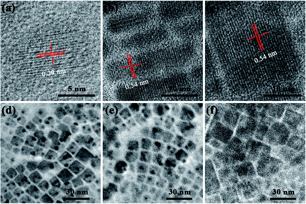 | ||
| Fig. 1 (a)–(c) Typical HRTEM images of CsPbCl3 NCs obtained using different reaction conditions. TEM images of cubic CsPbCl3 NCs after washing (d) two, (e) four, and (f) six times. | ||
It is found that monodispersed spherical CsPbCl3 quantum dots (QDs) are well-separated and uniform in size with diameter ∼5 nm. This is confirmed by transmission electron microscope (TEM), as shown in Fig. 1a. The high-resolution TEM (HR-TEM) imaging reveals that the QDs are highly crystalline in structure. As shown in Fig. 1a, the lattice fringes of the CsPbCl3 QDs have a spacing of ca. 0.31 nm, well in agreement with the interplane spacing of the cubic-phase CsPbBr3 for the (111) crystal planes.35 As the reaction time rises from 5 s to 10 s, colloidal CsPbCl3 platelet was formed with obvious morphology shown in Fig. 1b. Careful measurements indicate that the CsPbCl3 nanocubes are ca. 10 nm in length. The HR-TEM image reveals that the lattice fringe of a represent cubic is 0.54 nm, in consistent with the (001) plane of cubic crystal structure CsPbCl3.35 By further enhanced the reaction times (20 s), the CsPbCl3 cubics were synthesized. As presented in Fig. 1c. The HR-TEM image (Fig. 2f) highlights the CsPbCl3 cubics with a well-defined crystalline structure with a cubic lattice parameter of 0.54 nm, along with the crystalline direction of (001).35
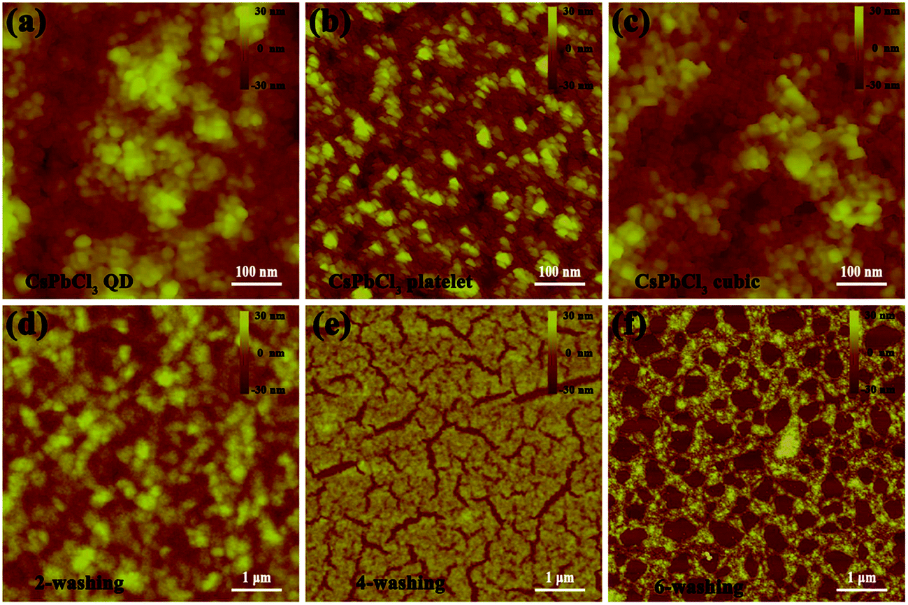 | ||
| Fig. 2 AFM images of the films fabricated using CsPbCl3 in (a) QD, (b) platelet, and (c) cubic form. AFM images of the film fabricated using cubic CsPbCl3 after washing (d) two, (e) four, and (f) six times. | ||
It is well known that the NC quality (purity and solubility) is important to fabricate large-area, crack-free, low-roughness perovskite thin films. Here, we demonstrated a highly efficient purification process involving using a hexane/methyl acetate (MeOAc) mixed solvent to control the surface ligand density on the CsPbCl3 NCs to realize the high purity and solubility. The transmission electron microscopy (TEM) images that obtained after washing the cubic CsPbCl3 NCs two, four, and six times are exhibited in Fig. 1d–f, respectively. The grain corners gradually become blurred as the number of washings increases. Thus, excessive purification resulted in obvious aggregation and precipitation due to the serious loss of surface ligands. Based on these results, it was decided to wash the CsPbCl3 NCs only two times for purification.36
In order to investigate the microstructure and morphology of the CsPbCl3 thin films, atomic force microscope (AFM) measurements were performed. Fig. 2a–c present AFM images of the individual films based on QD, platelet, and cubic CsPbCl3 NCs, respectively, and clearly reveal the small CsPbCl3 grains. Fig. 2d–f display AFM images of the films fabricated with CsPbCl3 cubic purified at different times (two, four, and six times, respectively). The film used the CsPbCl3 cubic that was washed twice is clearly smooth and uniform. However, the film became cracked after the cubic washing four times. Furthermore, washing six times caused a large number of holes to form in the cubic CsPbCl3 film, which would extend the carrier transport length. These results also indicate that the film quality is the best after washing twice.37
The cubic CsPbCl3 NC-based PD is illustrated schematically in Fig. 3a. The device contains a typical ITO/CsPbCl3 NCs/quartz stack: the CsPbCl3 NC film was fabricated by spin-coating approach with 100 nm thickness; afterwards, a pair of interdigitated ITO electrodes (100 nm thick) was thermally evaporated onto the films through a shadow mask, resulting in a channel width/length ratio of 200 μm/5 μm. Fig. 3b shows a typical X-ray diffraction (XRD) pattern of cubic CsPbCl3 NCs. Apparently, the CsPbCl3 crystallizes into a cubic structure (Pm3m space group) with no observable impurity phases.38 The absorption and photoluminescence (PL) spectra were measured and are presented in Fig. 3c. The CsPbCl3 NCs exhibit strong absorption from 300 nm to 410 nm and a narrow band-edge emission peak at 402 nm, which is consistent with the literature.39,40 The absorption implies that PDs based on CsPbCl3 NCs will intrinsically be visible-blind.
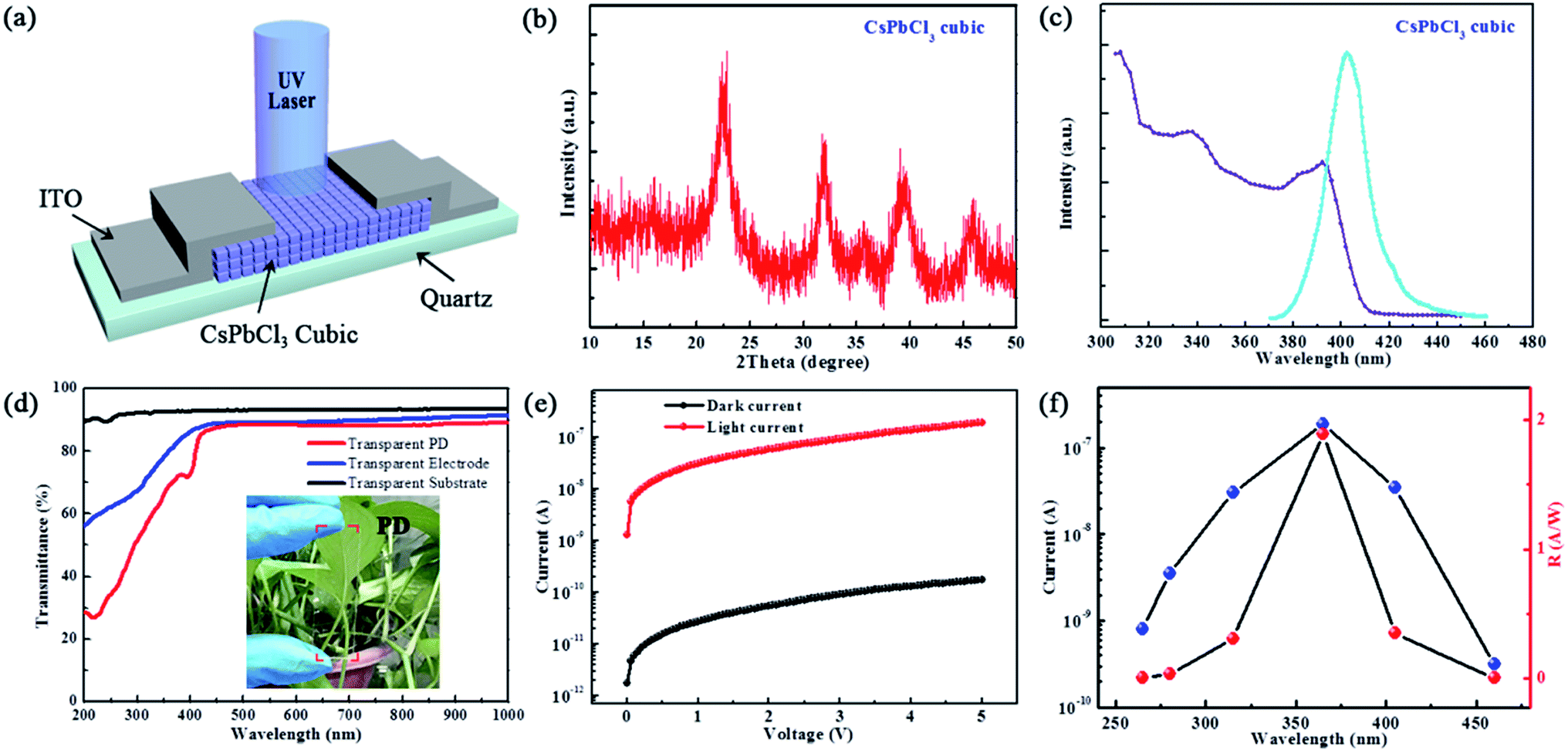 | ||
| Fig. 3 (a) Schematic of the device. (b) XRD pattern and (c) absorption and emission spectra of cubic CsPbCl3. (d) Transmittance spectra of the bare substrate, electrode, and PD device. (e) I–V logarithm curves of the PD device under 365 nm illumination (10 mW cm−2) and in darkness. (f) Photocurrent spectrum and R spectrum of the fabricated PD. | ||
The PD fabricated using cubic CsPbCl3 NCs shows approximately 90% optical transmittance in the visible light region. For comparison, the transmittance spectra of the bare substrate and transparent electrode are also collected in Fig. 3d. The worse transmittances of the transparent electrode and CsPbCl3 PD in the UV region, especially for the CsPbCl3 PD, are attributable to strong absorption in the UV region. The photograph inserted in Fig. 3d confirms that the PD has high transparency. Note that the green plants behind the transparent device can easily be seen. Fig. 3e provides the dark and light I–V curves of the CsPbCl3 PD, where the light curve was obtained under 365 nm illumination (10 mW cm−2). The device exhibits a high signal-to-noise ratio of about 103, implying that the PD is highly sensitive, which may be attributable to the high light-absorption efficiency of the CsPbCl3 NCs.41
The CsPbCl3 PD also exhibits high spectral selectivity (photocurrent and responsivity (R)), which can clearly be seen in Fig. 3f. The R is given by the following equation:42
 | (1) |
The time-dependent photoresponse of the PD measured by periodically turning it on and off in 5 s intervals is presented in Fig. 4a. The photocurrent rapidly increases to a stable peak value (1.89 × 10⁻⁷ A) upon the application of 365 nm illumination and then quickly decreases to its initial value (1.71 × 10⁻¹⁰ A) upon the light being turned off, revealing that the CsPbCl3 PD has highly stable and reproducible characteristics. It should be note that the rise time and decay time of the PDs are defined as the time taken for the initial current to increase or decrease to 90% of the peak value, respectively.44 The rise and decay times of the present device are 41 ms and 43 ms (Fig. 4b), respectively, indicating that the CsPbCl3 PD has ultra-fast responses compared to those the traditional transparent ZnO-based UV PDs, whose typical response speeds have been reported to be tens or hundreds of seconds (seen in Table 1).45–52 The on/off cycle testing results are depicted in Fig. 4c. After 1000 repeated on/off cycles, the on current (1.83 × 10⁻⁷ A) and off current (1.81 × 10⁻¹⁰ A) do not suffer any appreciable deterioration, and the device maintains a high on/off ratio above 103. These parameters are beneficial for practical applications.
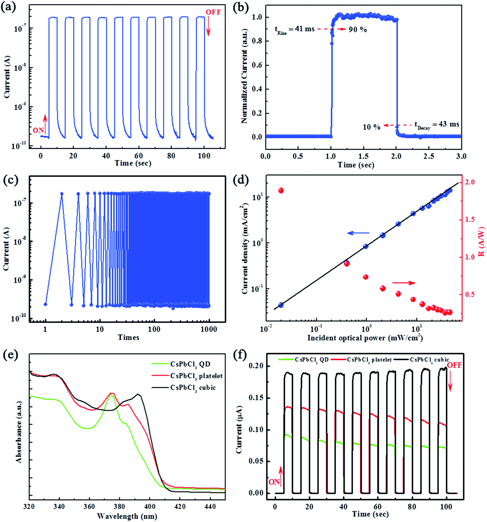 | ||
| Fig. 4 (a) On–off switching properties measured under 365 nm light illumination (10 mW cm−2) at a bias of 5 V. (b) Time-resolved photocurrent of the fabricated PD. (c) On–off cycling test results measured under 365 nm light illumination (10 mW cm−2) at a bias of 5 V. (d) Fit curve for photocurrent versus incident optical power. (e) Absorption spectra of CsPbCl3 in QD, platelet, and cubic form. (f) On–off switching properties of the PDs based on CsPbCl3 in QD, platelet, and cubic form. | ||
| Films | Rise time (s) | Decay time (s) | R (A W−1) | Reference |
|---|---|---|---|---|
| CsPbCl3 NC | 0.041 | 0.043 | 1.89 | This work |
| ZnO NC | 0.1 | 1 | 61 | 45 |
| ZnO–SnO2 nanofibers | 32.2 | 7.8 | — | 46 |
| LaAlO3 single crystal | — | — | 0.0718 | 47 |
| SrTiO3 single crystal | — | — | 0.213 | 48 |
| SrTiO3 single crystal | — | — | 0.03 | 49 |
| GaN film | 0.28 | 0.45 | 0.34 | 50 |
| NiO film | 0.266 | 0.2 | 4.5 | 51 |
| GdNiO3 | — | — | 0.23 | 52 |
Fig. 4d shows the photocurrent and photoresponsivity (R) as a function of the light intensity. The photocurrent increases as the illumination intensity increases, which is as expected since the number of photogenerated carriers is proportional to the absorbed photon flux. The fit line reveals that the photocurrent is proportional to the light intensity. In this study, the highest value of R was found to be 1.89 A W−1 upon device optimization. Compared with other traditional transparent materials based UV PDs (seen in Table 1),45–52 the remarkably photo-response performance by the CsPbCl3 PDs is attributed to its larger crystal size, which are favorable for carrier mobility, leading to enhanced photoresponse.
The absorbing properties of the QD, platelet, and cubic CsPbCl3 PDs as determined using UV-vis spectroscopy are presented in Fig. 4e. To the best of our knowledge, the optical bandgap increases as the NC size decreases.53,54 Therefore, the optical bandgap can be tuned by adjusting the reaction conditions in the CsPbCl3 NC synthesis process at 90 °C using various reaction temperatures.55 The optical absorption spectra of all of the PDs (Fig. 4e) show intense absorption in the UV region. Evidently, the optical bandgap of the CsPbCl3 NCs is redshifted as the crystal size increases (from QD, to platelet, to cubic), which is consistent with other reports.56
The I–t curves of the QD, platelet, and cubic CsPbCl3 PDs are presented in Fig. 4f for comparison. All of the PDs exhibit high current responses to the UV light and excellent on–off switching performances. The distinction among the three types of CsPbCl3 NCs is that the peak current intensity increases as the crystal size increases, since the carrier mobility increases simultaneously. Large particles will reduce the number of the interface defects, resulting in higher carrier mobility and photocurrent.57
Conclusions
In conclusion, we performed detailed analysis of the effects of employing CsPbCl3 NCs in assembled films and final devices using various characterization methods and finally successfully fabricated a high-performance transparent UV PD from solution-processed inorganic perovskite CsPbCl3 NCs. The strong UV absorption and high visible light transmittance indicate that the CsPbCl3-based UV PD is intrinsically visible-blind. As a result, the device exhibits good responsivity (1.89 A W−1), a high on/off ratio (103), and stable properties after 1000 repeated on/off cycles. Furthermore, the rise and decay times of the present device are 41 ms and 43 ms, respectively, indicating that CsPbCl3 PDs possess ultra-fast responses compared with the traditional transparent UV PDs. Finally, our investigation of the influence of using different sizes of CsPbCl3 crystals in UV PDs revealed that cubic CsPbCl3 crystals yield the highest photocurrent intensity due to the increase in carrier mobility with increasing size. All of these results demonstrate that inorganic perovskite CsPbCl3 NCs are among the most effective semiconductors for use in high-performance transparent UV PDs.Experimental section
Materials preparation
Synthesis of CsPbCl3 nanocrystals: Cs2CO3 (0.415 g), 1-octadecene (ODE, 18 ml), and oleic acid (OA, 1.76 ml) were added to a round-bottom flask and stirred under a vacuum for 30 min at 120 °C as Cs-oleate. PbCl2 (0.25 g), ODE (10 ml), OA (1.6 ml), and Oleylamine (OAm, 1.6 ml) were stirred in another round-bottom flask and degassed under a vacuum at 90 °C for 1 h before filling the flask with N2. Then, the Cs-oleate (0.8 ml) was swiftly injected into the reaction mixture at 90 °C. The reaction was quenched by immediate immersion of the flask into an ice bath for different times. The synthesized CsPbCl3 NCs (QD, platelet, and cubic) were precipitated by adding 200 ml MeOAc. This process was repeated twice, and the CsPbCl3 NCs were finally dispersed in hexane with a concentration of 50 mg ml−1.Device fabrication
The PD fabrication process was as follows: the CsPbCl3 layer was fabricated by spin-coating a solution of the relevant CsPbCl3 NCs (QD, platelet, or cubic) onto a cleaned quartz substrate at 2500 rpm for 15 s. To form the high-mobility and low-trap density CsPbCl3 layer, the prepared film was quickly dipped into a neat MeOAc solution and then a saturated Pb(OAc)2 MeOAc solution. This process was repeated four times, producing CsPbCl3 films with thicknesses of about 100 nm. All of the spin-coating steps were performed in ambient air. Finally, a pair of interdigitated ITO electrodes (100 nm thick) was thermally evaporated onto the films through a shadow mask, resulting in a channel width/length ratio of 200 μm/5 μm.Characterization
All of the electrical characteristics were recorded with an Agilent B2902A in ambient air. The monochromatic light was from a Newport Oriel 200™. Prior to the utilization of the light, the spectral and the light intensity were calibrated using a mono-silicon detector. The TEM images were taken by a JEM-2100 JEOL TEM. The surface morphology was characterized by using an AFM (Dimension ICON). The thickness of the films was determined using a Profilometer. UV-vis spectra were recorded using a JASCO V-570 spectrophotometer. The samples were excited by a laser (Omni-λ300), with a wavelength of 365 nm. The mechanical optical choppers are used to control the laser on/off. The phase compositions of the samples were characterized by a DX-2700 XRD using Cu Kα radiation (λ = 0.15418 nm) in a 2θ range of 10–50°.Conflict of interest
The authors declare no competing financial interests.Acknowledgements
This work was supported by the National Nature Science Foundation of China (61674098), the China Postdoctoral Science Foundation (2016M602759 and 2017M613052), the National Key Research Program of China (2016YFA0202403 and 2017YFA0204800), the 111 Project (B14041), the National University Research Fund (GK201703026), the Innovative Research Team (IRT_14R33) and the Chinese National 1000-talent-plan program (Grant No. 111001034).References
- J. F. Wager, Transparent Electronics, Springer, US, 2008 Search PubMed
.
- N. Nasiri, et al., Nanoscale, 2017, 9, 2059–2067 RSC
- G. A. Salvatore, et al., Nat. Commun., 2014, 5, 2982 Search PubMed
- J. Sun, et al., Adv. Funct. Mater., 2011, 21, 29–45 CrossRef CAS
- X. Zhang, et al., Nanoscale, 2017, 9, 6278–6285 RSC
- P. Hu, et al., Nano Lett., 2013, 13, 1649–1654 CrossRef CAS PubMed
- J. Wang, et al., Nanoscale, 2014, 6, 10734–10739 RSC
- Z. Jin, et al., Sci. Rep., 2014, 4, 4268 CrossRef PubMed
- M. Patel, et al., Adv. Electron. Mater., 2015, 1, 1500232 CrossRef
- B. Sun and H. Sirringhaus, Nano Lett., 2005, 5, 2408–2413 CrossRef CAS PubMed
- K. Ellmer and A. Klein, ZnO and Its Applications, Springer Berlin Heidelberg, 2008 Search PubMed
- J. Lu, et al., Nanoscale, 2015, 7, 3396–3403 RSC
- D. Gedamu, et al., Adv. Mater., 2014, 26, 1541–1550 CrossRef CAS PubMed
- Y. K. Mishra, et al., ACS Appl. Mater. Interfaces, 2015, 7, 14303–14316 CAS
- A. Bera and D. Basak, ACS Appl. Mater. Interfaces, 2009, 1, 2066–2070 CAS
- D.-Y. Guo, et al., Sci. Rep., 2014, 4, 7469 CrossRef CAS PubMed
- K. Liu, et al., J. Phys. Chem. C, 2010, 114, 19835–19839 CAS
- Z. Qi, et al., Adv. Electron. Mater., 2015, 1, 1500173 CrossRef
- J. Jiang, et al., J. Mater. Chem. A, 2017, 5, 9514–9522 CAS
- D. Yang, et al., Adv. Mater., 2016, 28, 5206–5213 CrossRef CAS PubMed
- G. Maculan, et al., J. Phys. Chem. Lett., 2015, 6, 3781–3786 CrossRef CAS PubMed
- V. Adinolfi, et al., Adv. Mater., 2016, 28, 7264–7268 CrossRef CAS PubMed
- G. E. Eperon, et al., Energy Environ. Sci., 2014, 7, 982–988 CAS
- S. D. Stranks and H. J. Snaith, Nat. Nano, 2015, 10, 391–402 CrossRef CAS PubMed
- D. Bi, et al., Sci. Adv., 2016, 2, e1501170 Search PubMed
- J. Burschka, et al., Nature, 2013, 499, 316–319 CrossRef CAS PubMed
- H. Zhang, et al., Adv. Funct. Mater., 2017, 27, 1604382 CrossRef
- Q. Wang, et al., ACS Energy Lett., 2017, 2, 1479–1486 CrossRef CAS
- J. Liang, et al., J. Am. Chem. Soc., 2016, 138, 15829–15832 CrossRef CAS PubMed
- A. Swarnkar, et al., Science, 2016, 354, 92–95 CrossRef CAS PubMed
- X. Li, et al., Small, 2017, 13, 1603996 CrossRef PubMed
- X. Li, et al., Adv. Funct. Mater., 2016, 26, 2435–2445 CrossRef CAS
- W. Liu, et al., J. Am. Chem. Soc., 2016, 138, 14954–14961 CrossRef CAS PubMed
- T. Udayabhaskararao, et al., Chem. Mater., 2017, 29, 1302–1308 CrossRef CAS
- S. Sun, et al., ACS Nano, 2016, 10, 3648–3657 CrossRef CAS PubMed
- J. Li, et al., Adv. Mater., 2017, 29, 1603885 CrossRef PubMed
- X. Li, et al., Adv. Funct. Mater., 2016, 26, 5903–5912 CrossRef CAS
- N. S. Makarov, et al., Nano Lett., 2016, 16, 2349 CrossRef CAS PubMed
- D. Amgar, et al., Nano Lett., 2017, 17, 1007–1013 CrossRef CAS PubMed
- G. Nedelcu, et al., Nano Lett., 2015, 15, 5635–5640 CrossRef CAS PubMed
- Z. Jin, et al., ACS Appl. Mater. Interfaces, 2016, 8, 33043–33050 CAS
- L. Dou, et al., Nat. Commun., 2014, 5, 5404 CrossRef CAS PubMed
- Y. Liu, et al., Adv. Mater., 2016, 28, 9204–9209 CrossRef CAS PubMed
- Z. Jin and J. Wang, J. Mater. Chem. C, 2014, 2, 1966–1970 RSC
- Y. Jin, et al., Nano Lett., 2008, 8, 1649–1653 CrossRef CAS PubMed
- W. Tian, et al., Adv. Mater., 2013, 25, 4625–4630 CrossRef CAS PubMed
- J. Xing, et al., Opt. Lett., 2009, 34, 1675 CrossRef CAS PubMed
- E. J. Guo, et al., Appl. Opt., 2010, 49, 2557–2560 CrossRef CAS
- J. Xing, et al., Opt. Lett., 2007, 32, 2526–2528 CrossRef CAS PubMed
- A. Gundimeda, et al., Appl. Phys. Lett., 2017, 110, 103507 CrossRef
- A. A. Ahmed, et al., Sens. Actuators, A, 2017, 262, 78–86 CrossRef CAS
- L. Wang, et al., Appl. Phys. Lett., 2017, 110, 043504 CrossRef
- Z. Jin, et al., Adv. Funct. Mater., 2016, 26, 5284–5289 CrossRef CAS
- L. Protesescu, et al., Nano Lett., 2015, 15, 3692–3696 CrossRef CAS PubMed
- Z. Jin, et al., Sci. Rep., 2016, 6, 37106 CrossRef CAS PubMed
- Z. Liang, et al., ACS Appl. Mater. Interfaces, 2016, 8, 28824–28830 CAS
- Z. Jin, et al., Adv. Mater., 2016, 28, 3697–3702 CrossRef CAS PubMed
| This journal is © The Royal Society of Chemistry 2017 |