
 Open Access Article
 This Open Access Article is licensed under a Creative Commons Attribution-Non Commercial 3.0 Unported Licence
Aim and shoot: molecule-imprinting polymer coated MoO3 for selective SERS detection and photocatalytic destruction of low-level organic contaminants†
Lingzhi Wang *a,
Yin Xua,
Xianjun Tana,
Sen Tapasb and
Jinlong Zhang*a
*a,
Yin Xua,
Xianjun Tana,
Sen Tapasb and
Jinlong Zhang*a
aKey Laboratory for Advanced Materials, Institute of Fine Chemicals, East China University of Science and Technology, 130 Meilong Road, Shanghai 200237, P. R. China. E-mail: wlz@ecust.edu.cn; jlzhang@ecust.edu.cn
bCentre for Materials Science, Institute of Nanotechnology and Bioengineering, School of Forensic and Investigative Sciences, University of Central Lancashire, Preston, UK
First published on 21st July 2017
Abstract
A sensitive and selective SERS sensor with easy and excellent recyclability is highly demanded because of its great potential application in complex detection environments. Here, using methylene blue (MB) as a model target, a semiconductor-based SERS substrate composed of a MoO3 nanorod core and a uniform molecule-imprinting polymethacrylic acid shell (MIP) with a thickness of 4 nm was designed and fabricated (MoO3@MIP) to achieve selective detection. The key to the successful coating of the ultrathin uniform MIP shell lies in the pretreatment of a MoO3 core with nitric acid, providing sufficient surficial hydroxyls for the anchoring of a polymer precursor. The molecule-imprinted voids for MB were formed simply via light irradiation as a result of photocatalytic degradation by a MoO3 semiconductor. This core–shell MIP composite shows a high SERS selectivity towards low-level MB in a mixed MB/CV solution. The enhanced factor (EF) is high, at 1.6 × 10⁴. More importantly, the selective detection allows the further photocatalytic recycling of MoO3@MIP in an “aim-and-shoot” way, which well preserves the detection selectivity and sensitivity towards MB at least for 4 cycles. Based on decreased sensitivity with the increasing shell thickness (10–24 nm), a MIP-gating charge transfer mechanism is proposed to demonstrate the high EF instead of the molecule-enrichment effect. This “aim-and-shoot” strategy is expected to push forward the prosperous application of selective SERS for trace detection in versatile environments.
1. Introduction
Surface-enhanced Raman scattering (SERS) is an extremely sensitive and rapid analytical tool for the detection of molecules in the fields of chemistry, biology, medicine, environmental monitoring, etc.1–7 In recent years, SERS has attracted considerable attention since it can reveal structure, composition and concentration of target molecules even at a single-molecule level by measuring fingerprint characteristic vibrations of molecules.8–11 However, high sensitivity is not the only factor for a satisfactory SERS sensor during the practical application, other significant factors including tunable selectivity, high stability and multiple recyclability are also desirable. In particular, in consideration of the complicated fingerprint spectrum from each molecule, it is highly challenging to selectively identify a specific target from a variety of interference species, especially for ones with low concentrations.The molecule-imprinting technique (MIT) has witnessed a tremendous advance in chemical and biological sensors because of the remarkable selectivity and affinity towards target molecules.12–15 Interest in combining molecule-imprinting polymers (MIPs) with SERS has recently surged for the significantly improved selectivity of the substrate besides the sensitivity. For examples, Bompart et al. have reported a nanosensor for the determination of (S)-propranolol based on MIP and SERS.16 Holthoff et al. prepared a SERS substrate based on MIT for the highly selective detection of 2,4,6-trinitrotoluene (TNT).17 Chang et al. demonstrated that surface-imprinted core–shell Ag nanoparticles can significantly improve the sensitivity for SERS detection of 4-mercaptobenzoic acid.18 Lv et al. fabricated a thin imprinted polymer layer on the surface of gold nanobelts for selective SERS detection of protein biomarkers.19 The current study relevant to the combination of SERS and MIPs are generally limited to noble metals of Ag and Au.16–19 Unfortunately, the noble metals have drawbacks including high-cost, low biocompatibility, poor reusability and instability, which largely restrict their wide applications.20–22 Great effort has been devoted to improve the application performance of noble metal substrates. For example, nanocomposites combining plasmonic metal with semiconductor have been elaborately designed to achieve a photocatalytic recyclability.23–27 On the other hand, semiconductor materials such as α-Fe2O3, Cu2O, MoO3−x, TiO2, and MoS2 actually have also been revealed to be SERS-active.28–33 However, up to now, no selective and recyclable SERS substrate simply based on semiconductor has been designed mainly due to the low sensitivity.
Herein, selective and high sensitive SERS substrate based on MoO3 nanorod was fabricated through the finely controllable coating of an ultrathin molecule-imprinting polymethacrylic acid layer. The prerequisite for the successful coating is an acid pretreating of MoO3, forming abundant hydroxyls for the anchoring of silane coupling agent, 3-methacryloxypropyltrimethoxysilane (MPS). The MoO3 nanorods were adopted due to its easy synthesis, low cost, excellent chemical stability and nontoxicity. MB was used as a model target and embedded into the polymer shell by directly involving into the coating process. Through a simple light irradiation, MB was photocatalytically eliminated, leaving memory voids inside the shell. This core–shell structured MoO3@MIPs exhibits high selectivity towards MB with an enhanced factor of 1.6 × 10⁴, which is resulted from the MIP-gating charge transfer between MoO3 and MB instead of the molecule-enrichment effect. Finally, this selectively “aimed” MB molecules can be photocatalytically eliminated (shot). The recycled substrate through the unique “aim-and-shoot” way can well preserve its detection performance at least for 4 cycles.
2. Experimental section
2.1 Materials
Molybdenum powder, 3-methacryloxypropyltrimethoxysilane (MPS), hydrogen peroxide (H2O2, 30 wt%), acetonitrile (ACN), methanol (MeOH), crystal violet (C25H30N3Cl; CV) and methylene blue (C16H18N3SCl; MB) was bought from Aladdin, ethyl alcohol, acetic acid (CH3COOH), nitric acid (HNO3), N,N′-methylene diacrylamide (MBA), azobisisobutyronitrile (AIBN) and methacrylic acid (MAA) was purchased from Sigma-Aldrich. All chemical reagents were of analytical grade and the water used in all experiments was ultrapure water.2.2 Preparation of SERS substrates
![[thin space (1/6-em)]](https://www.rsc.org/images/entities/char_2009.gif) :1, v/v) solution, then 1 mL of MPS was dropwise added into the above solution. The mixture was heated at 80 °C for 24 h under nitrogen protection in order to modify MoO3 nanorods with MPS. The product (MoO3–MPS) was washed with ethanol and dried under vacuum at 60 °C for 12 h. The MoO3@MIPs hybrid was produced by distillation–precipitation polymerization: the template MB (0.02 g) and the functional monomer MAA (0.1 mL) were dissolved in ACN (80 mL) in a 100 mL round-bottom flask. MoO3–MPS (200 mg), MBA (0.088 g) as the cross linking agent, and AIBN (0.02 g) as the initiator were added to the solution. The mixture was stirred at room temperature for 30 min. Then the reaction system was proceeded in distilling apparatus at 90 °C for about 6 h after 40 mL of the acetonitrile was distilled. The as-made composite was washed with acetonitrile and methanol–acetic acid (4:1, v/v) solution to remove the surficial MB. Then the remaining MB embedded the shell was further degraded under a 300 W xenon lamp equipped with a solar simulator for several times. For comparison purpose, the non-imprinted MoO3@NIPs nanocomposites were prepared in the absence of the template MB using the same method.
:1, v/v) solution, then 1 mL of MPS was dropwise added into the above solution. The mixture was heated at 80 °C for 24 h under nitrogen protection in order to modify MoO3 nanorods with MPS. The product (MoO3–MPS) was washed with ethanol and dried under vacuum at 60 °C for 12 h. The MoO3@MIPs hybrid was produced by distillation–precipitation polymerization: the template MB (0.02 g) and the functional monomer MAA (0.1 mL) were dissolved in ACN (80 mL) in a 100 mL round-bottom flask. MoO3–MPS (200 mg), MBA (0.088 g) as the cross linking agent, and AIBN (0.02 g) as the initiator were added to the solution. The mixture was stirred at room temperature for 30 min. Then the reaction system was proceeded in distilling apparatus at 90 °C for about 6 h after 40 mL of the acetonitrile was distilled. The as-made composite was washed with acetonitrile and methanol–acetic acid (4:1, v/v) solution to remove the surficial MB. Then the remaining MB embedded the shell was further degraded under a 300 W xenon lamp equipped with a solar simulator for several times. For comparison purpose, the non-imprinted MoO3@NIPs nanocomposites were prepared in the absence of the template MB using the same method.2.3 Characterizations
The transmission electron microscopy (TEM) was performed on a JEOL 2100 LaB6 TEM, at an accelerating voltage of 200 kV. The morphologies of the samples were obtained using scanning electron microscope (SEM) (JSM-6360LV). The X-ray diffraction (XRD) spectrum analysis of MoO3@MIPs was performed on a Rigaku D/max 2550 VB/PC apparatus. Fourier transform infrared spectra (FT-IR) were recorded with a Nicolet Avatar 360 spectrometer (USA).2.4 Adsorption experiment
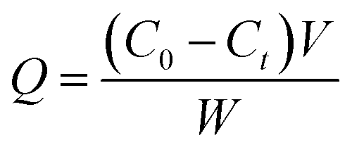
5 mg MoO3@MIPs or MoO3@NIPs nanocomposites were placed in a round-bottom flask which mixed with 20 mL MB solution with initial concentrations of 32 mg L−1. The mixture was stirred in a thermostatic oscillator for 5 h at 25 °C. The concentration of MB was measured by UV-vis spectrometer. The adsorption capacity (Q) of MoO3@MIPs or MoO3@NIPs was calculated as follows:39where C0 (mg L−1) is the initial concentration of MB, Ct (mg L−1) is the MB concentration at the time t, V (L) is the volume of solution, and W (g) is the mass of the MoO3@MIPs or MoO3@NIPs.
2.5 Measurements of SERS sensitivity
Raman spectra were evaluated by a micro-Raman system (Renishaw inVia-Reflex). Before SERS measurements, 5 mg of MoO3@MIPs hybrid were added to 1 mL of MB solution in a centrifuge tube for 30 min. Then 20 μL of the mixture were transferred to a glass slide (35 mm × 25 mm scale) and dried in dark naturally. Raman spectra were obtained using 532 nm laser (0.5% power) as the excitation light source with 50× objective. And the accumulation time was 10 s.2.6 Recyclability experiment
The substrates were recycled by photo-degradation after SERS characterization of the MB adsorbed on MoO3@MIPs: 100 μL of water was dropped on the used substrates. Then the substrate was irradiated with a 300 W xenon lamp equipped with a solar simulator (AM 1.5) for 30 min, and dried in air. The following Raman spectra were produced to evaluate the degradation degree of MB. This process was continued until no Raman signal of MB could be found. The cycles were repeated for four times on each sample to check the reusability characterization of MoO3@MIPs.2.7 Enhancement factor (EF) measurement
20 μL of the mixture of MoO3@MIPs and 10−5 M MB was dropped on the glass slide and dried at room temperature. As a comparison, 20 μL of 10−2 M MB aqueous solution was dropped on a glass slide. Raman spectra were obtained using 532 nm laser (0.5% power) as the excitation light source with 50× objective, and the accumulation time was 10 s.3. Results and discussion
3.1 Preparation and characterization of MoO3@MIPs
The fabrication route to MoO3@MIPs is shown in Scheme 1. First, MoO3 nanorods were synthesized via a hydrothermal process, which were then dispersed in HNO3 solution to form surficial hydroxyls for the further anchoring of MPS through an ester exchange reaction (MoO3–MPS). The MoO3–MPS was coated with a MB encapsulated polymethacrylic acid layer, and then the embedded MB was eliminated through light irradiation to form molecule imprinting voids.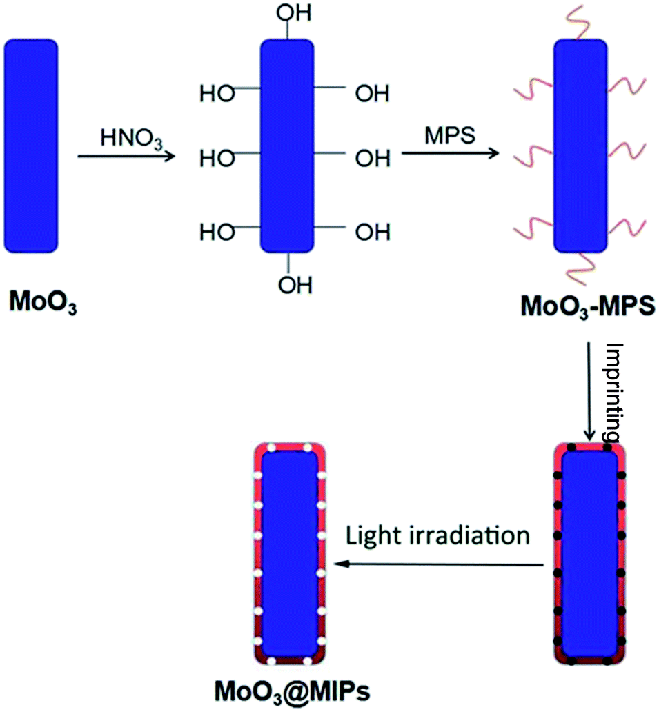 | ||
| Scheme 1 Schematic diagram for synthetic process of MoO3@MIPs. | ||
The SEM images indicate both of MoO3 and MoO3@MIPs are monodispersed one-dimensional nanorods (Fig. 1a and b). The TEM image of MoO3 (Fig. 1c) reveals a width of ca. 170 nm and a length of ca. 10 μm. A thin uniform polymer shell with a thickness of ca. 4 nm can be observed after the coating (Fig. 1d). No obvious morphological change is found before and after the polymer coating. In contrast, the absence of HNO3 treatment leads to a non-uniform coating of polymer shell (Fig. S1†).
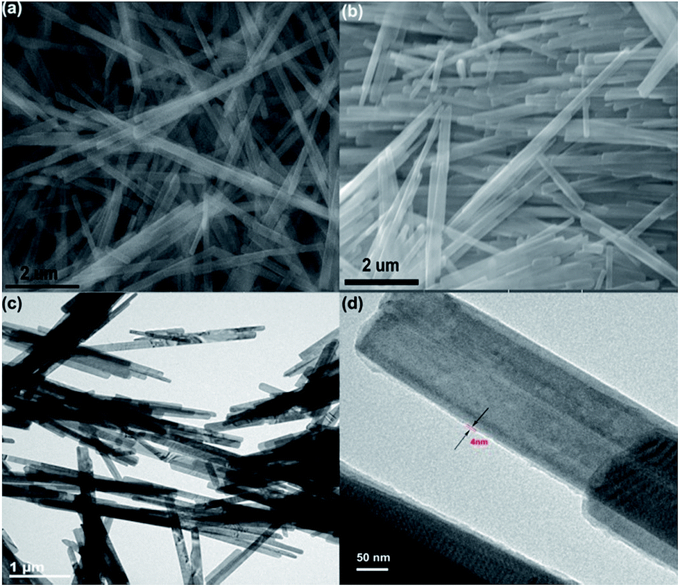 | ||
| Fig. 1 SEM and TEM images of MoO3 nanorods (a, c); SEM and TEM images of MoO3@MIPs (b, d). | ||
The crystal structure of MoO3 and MoO3@MIPs nanorods were characterized by XRD analysis (Fig. 2), where the dominant diffraction peaks at 2θ = 12.91°, 23.69°, 26.00°, 27.61°, 39.39°, 46.51°, and 59.10°, correspond well to the indices of (020), (110), (040), (021), (060), (210), and (081) planes of orthorhombic MoO3 phase (JCPDS card no. 05-0508), respectively. MoO3@MIPs show similar but weaker diffraction peaks due to the presence of a polymeric shell.
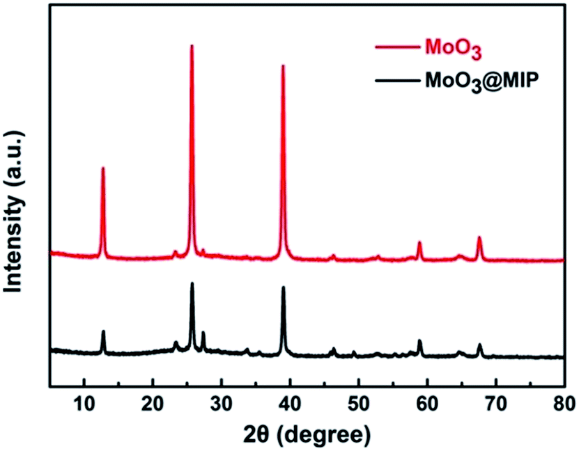 | ||
| Fig. 2 XRD patterns of the MoO3 and MoO3@MIPs nanorods. | ||
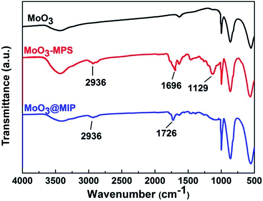
The FT-IR spectra indicate all the MoO3-based samples before and after modification show characteristic bands of MoO3 at 3437, 1629, 997, 864, and 560 cm−1 (Fig. 3). For MoO3–MPS, additional bands appear at 1696 cm−1, 2936 cm−1 and 1129 cm−1, which are arisen from C![[double bond, length as m-dash]](https://www.rsc.org/images/entities/char_e001.gif) O, –CH3 and –Si–O–C– groups, demonstrating MPS has been successfully modified on the surface of MoO3. For MoO3@MIPs, the strong absorption peak at 1731 cm−1 is assigned to the bending vibration of carboxyl group, confirming the formation of polymethacrylic acid on the surface of MoO3–MPS.
O, –CH3 and –Si–O–C– groups, demonstrating MPS has been successfully modified on the surface of MoO3. For MoO3@MIPs, the strong absorption peak at 1731 cm−1 is assigned to the bending vibration of carboxyl group, confirming the formation of polymethacrylic acid on the surface of MoO3–MPS.
 | ||
| Fig. 3 FT-IR spectra of the MoO3 nanorods, MoO3–MPS, and MoO3@MIPs. | ||
X-ray photoelectron spectroscopy (XPS) measurements were further performed to verify the surface composition. Fig. S2† shows the XPS survey spectra of MoO3 nanorods before and after treating with HNO3. The O 1s region of the samples can be fitted into two peaks at 530.04 eV and 531.82 eV attributed to molybdenum–oxygen bonds and the surface hydroxyls, respectively (Fig. 4a and b). It is obvious that the HNO3 treatment leads to the appearance of more –OH groups, verifying the uniform coating of polymer shell is related to the existence of abundant surficial –OH groups. Moreover, compared with the XPS survey spectrum of MoO3, new peak appear at approximately 101.6 eV (Si 2p) for sample MoO3–MPS, confirming the successful anchoring of MPS on MoO3 nanorods (Fig. 4c). The content of C increases to 35.32% up from 19.17% while that of Si decreases to 3.06% down from 9.12% when the MIP layers are further coated onto the MoO3–MPS surface (Fig. 4d).
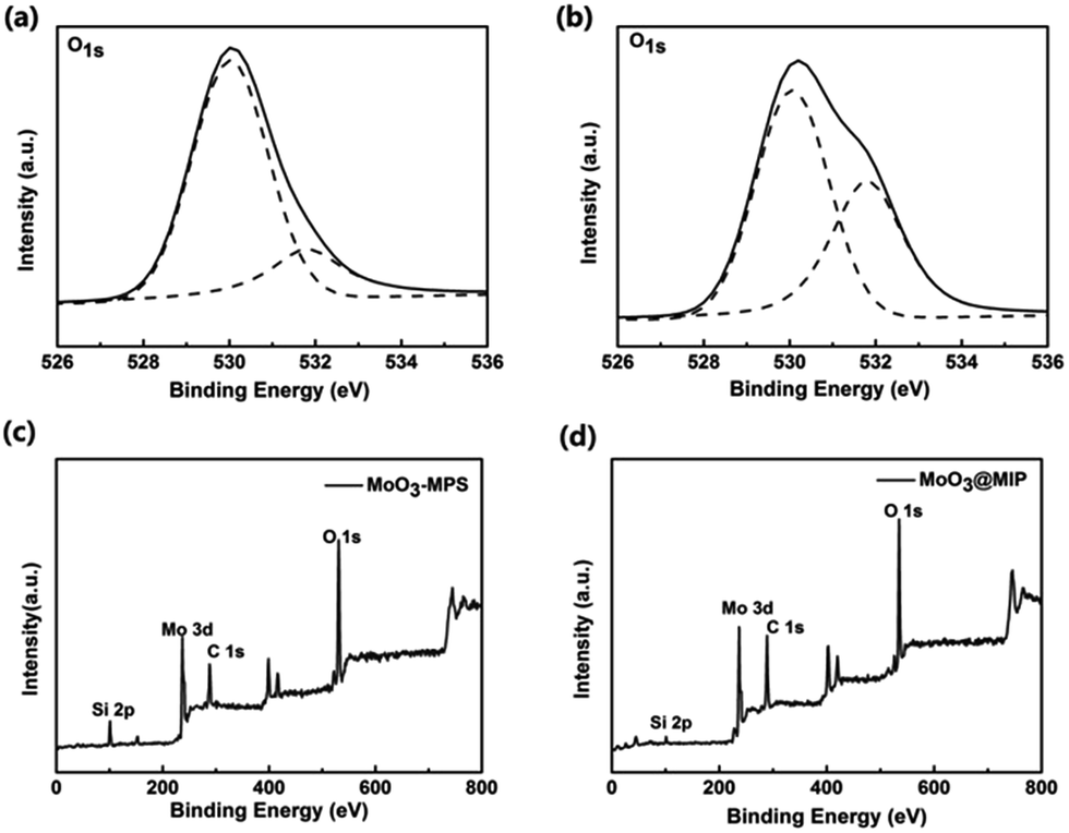 | ||
| Fig. 4 XPS spectra of O 1s for MoO3 (a) and MoO3–HNO3 (b); survey spectra of MoO3–MPS (c) and MoO3@MIPs (d). | ||
3.2 Rebinding performances of MoO3@MIPs
The adsorption experiments were carried out to evaluate the rebinding ability of MoO3@MIPs for MB. Fig. 5a presents the adsorption kinetics curves of MoO3@MIPs and MoO3@NIPs for MB. The MoO3@MIPs binding capacity for MB is about 77 mg g−1, much higher than that for MoO3@NIPs (27 mg g−1). In addition, the adsorption equilibrium is easily reached within 40 min for MoO3@MIPs and 70 min for MoO3@NIPs. These results verify that the MIP layers indeed possess imprinted cavities with enrichment ability for MB. MoO3@MIPs exhibits much higher adsorption capacity for MB than that for CV, while the amount of MB and CV adsorbed on MoO3@NIPs is almost the same (Fig. 5b), demonstrating the excellent selective adsorption capacity of MoO3@MIPs towards the target molecule MB.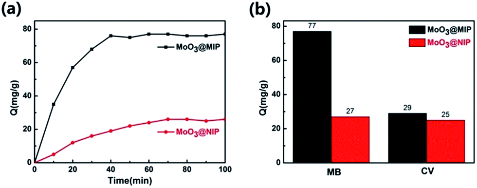 | ||
| Fig. 5 (a) Adsorption kinetics curves of MoO3@MIPs and MoO3@NIPs for MB; (b) adsorption capacities of MoO3@MIPs and MoO3@NIPs for MB and CV. | ||
3.3 SERS sensitivity of the MoO3@MIPs
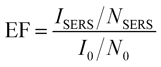
Fig. 6 presents the SERS spectra of MB using MoO3@MIPs and MoO3@NIPs as substrates. Strong signal of MB with a concentration of 10−5 M can be observed from MoO3@MIPs. When the concentration is decreased to 10−6 M, the signal of MB is still clearly present (Fig. 6a). In contrast, the band intensity of MB (10−5) significantly decreases when MoO3@NIPs was used and no signal of MB can be observed at a lower concentration (Fig. 6b, 10−6 M). Fig. S3a† presents the standard curve of MB. The above results well demonstrate the sensitivity of MoO3@MIPs towards the detection of MB. The enhancement factor (EF) for MB on MoO3@MIPs substrate is further evaluated by the following equation:34where ISERS and I0 are the intensities of the Raman peaks from the SERS and normal Raman spectra. NSERS and N0 are the average numbers of detected molecules in SERS and normal Raman measurement. The SERS spectra of MB detected on MoO3@MIPs substrate and glass slide are shown in Fig. S3b.† The calculated EF of MoO3@MIPs is 1.6 × 10⁴, which is hard to be obtained simply from the semiconductor substrates.
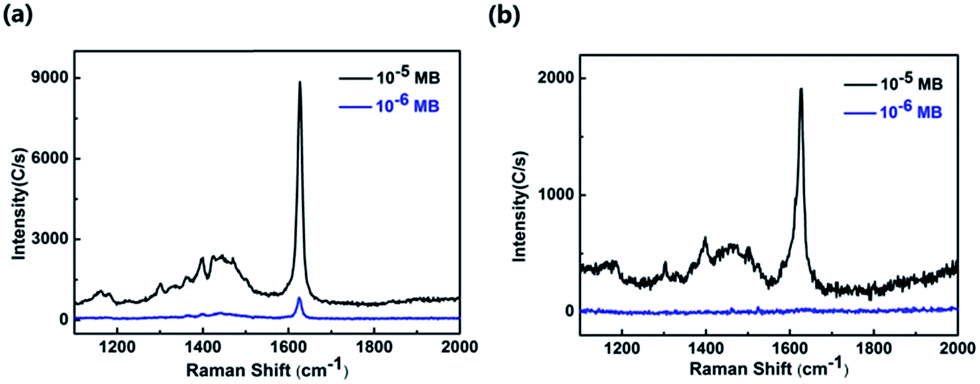 | ||
| Fig. 6 SERS spectra of MB from MoO3@MIPs (a) and MoO3@NIPs (b). | ||
3.4 SERS selectivity of the MoO3@MIPs
To testify the selectivity of MoO3@MIPs for MB, CV with similar molecule structure was adopted as a control. Fig. 7 shows SERS spectra of MB and CV on MoO3@MIPs and MoO3@NIPs. Weak SERS signals of CV (10−5 M) with a comparable intensity can be observed from MoO3@MIPs and MoO3@NIPs (inset, Fig. 7a), which both disappear at a lower concentration (Fig. S4,† 10−6 M), demonstrating the non-selectivity of MoO3@MIPs towards CV. For the mixture composed of equivalent MB and CV (10−5 M), strong SERS signal characteristics of MB is clearly observed, accompanied by a weak peak at 1588 cm−1 attributed to the carbon skeleton vibration of CV (Fig. 7a). Only MB can be detected when the concentrations of MB and CV both decreases to 10−6 M, further verifying the selective sensing ability of MoO3@MIPs towards MB. In order to exclude the randomness, the SERS intensity ratio of the peak at 1400 cm−1 and 1588 cm−1 obtained from the 10−5 M MB/CV mixture were measured. The relative standard deviation (RSD) of SERS intensity ratio is about 9.5% as determined from the SERS spectra of the 10−5 M MB/CV mixture (Fig. 7b), which are collected from 10 random sites on the same substrate (Fig. S5†).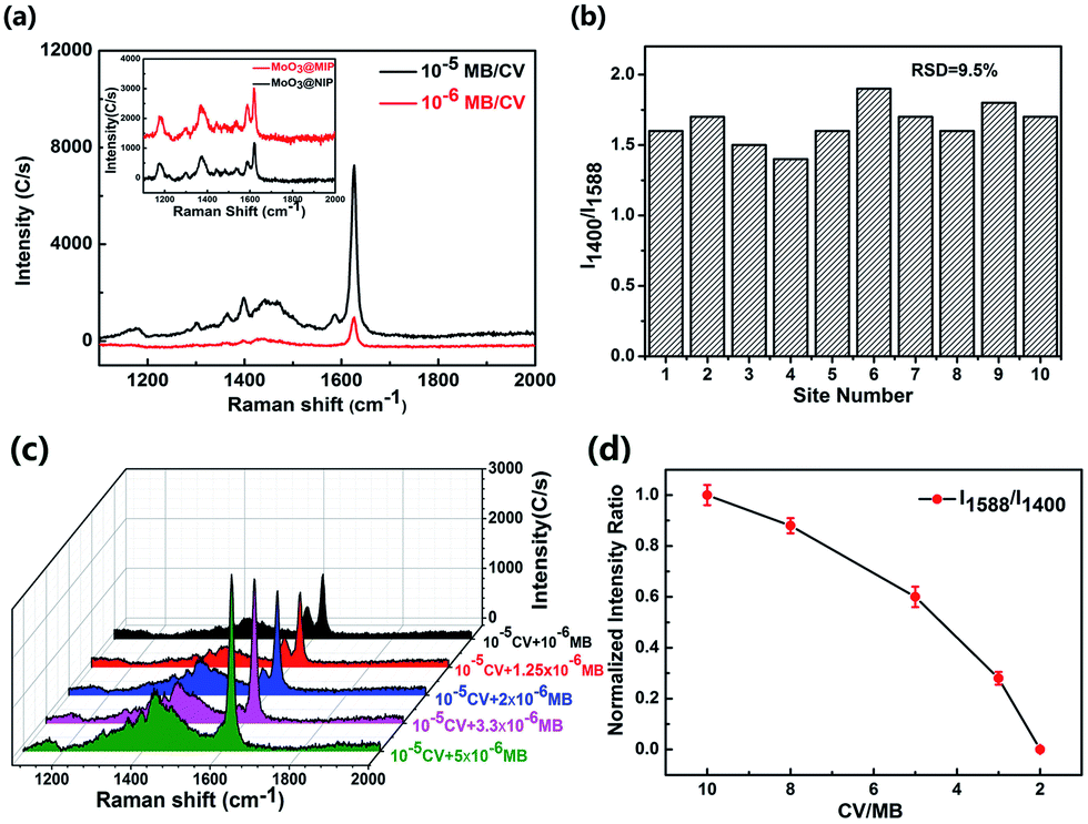 | ||
| Fig. 7 (a) SERS spectra of 10−6 M and 10−5 M of MB/CV mixtures on MoO3@MIPs. Inset: SERS spectra of CV (10−5 M) on MoO3@MIPs and MoO3@NIPs; (b) intensity ratio of the peak at 1400 cm−1 and 1588 cm−1 on 10 measured sites and the calculated RSD; (c) SERS spectra of mixtures composed of 10−5 M CV and lower level of MB (10−6 to 5 × 10⁻⁶ M); (d) relationship between normalized I1588/I1400 and CCV/MB. For every detected sample, SERS spectra were obtained from ten different spots. To exclude the interference from surficial molecules, the MoO3@MIP substrates immersed from the mixture of CV and MB were washed with acetonitrile and methanol–acetic acid (4:1, v/v) solution. | ||
To further demonstrate the selectivity of MoO3@MIP towards MB, the SERS spectra of mixed solutions with a fixed CCV (10−5 M) and a lower CMB (10−6 to 5 × 10⁻⁵ M) were recorded, where the signal of MB can always be clearly observed although CMB keeps lower than CCV (Fig. 7c). To more distinctly reveal the selectivity, the intensity ratio of bands at 1558 cm−1 (ICV) and 1400 cm−1 (IMB) for the spectrum collected at CCV/MB = 10 was normalized, the decrease of CCV/MB from 10 to 2 causes the dramatic reduction of ICV/IMB from 1 to 0 (Fig. 7d). The above results well prove the excellent selective performance of MoO3@MIPs towards target molecules.
3.5 Recyclability and stability of MoO3@MIPs substrates
In addition to the sensitivity and selectivity, the recyclability of SERS substrates is also important for reducing cost and increasing resource use efficiency in practical applications. During the preparation process, photocatalysis of the MoO3 core has proven to be effective in degrading embedded MB. Therefore, the recycling experiment was further proceeded by the following steps: after one cycle of SERS detection for MB, the substrates was irradiated by simulated sunlight for a certain time, and then re-conducted SERS analysis. Fig. 8a shows that no obvious MB peaks are found after 90 min irradiation, which indicates that the target molecules are completely decomposed. After 4 cycles of detection-irradiation process, there is no obvious decline in the SERS intensity of MB, suggesting the good stability and reusability of the MoO3@MIPs substrate.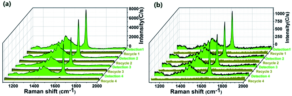 | ||
| Fig. 8 (a) SERS spectra of 10−5 M MB on MoO3@MIPs before and after self-cleaning for 4 cycles; (b) SERS spectra of the mixture of 10−6 M MB and CV on MoO3@MIPs before and after self-cleaning for 4 cycles. | ||
Moreover, the selective detection of MB in a mixed MB/CV solution demonstrate MB can be readily extracted into the MIP layer and inside locked, which further allows a selectively photocatalytic elimination of embedded MB in a precise “aim-and-shoot” way. To investigate the “aim-and-shoot” effect on refreshing the detection performance of MoO3@MIPs, the recycling experiment was further carried out in a mixed solution (10−6 M). Fig. 8b shows that no obvious MB peaks can be detected from the first-run used MB/MoO3@MIPs after 45 min irradiation, implying the total elimination of adsorbed MB from 10−6 M MB/CV mixture. After 4 cycles of detection-refresh, there is no obvious decline in the selective SERS performance, demonstrating the excellent recyclability of MoO3@MIPs through the “aim-and-shoot” way.
3.6 Mechanism
In order to study the SERS mechanism, the enrichment effect of the MIP shell thickness on the SERS activity was further explored. Fig. S6† shows core–shell MoO3@MIP nanorod with shell thicknesses in the range of 4–24 nm. Since the precursor concentration for the generation of MIP voids is set to be excessive (see Experimental section), the MIP void is assumed to be uniformly distributed in the shell. It is obvious the peak intensity of MB significantly decreases with the increasing shell thickness (Fig. 9a), demonstrating the signal enhancement is not governed by the molecule-enrichment effect. The specific relation between the detection sensitivity and the MIP voids density in a fixed objective Raman lens (1 μm) was further plotted by normalizing the intensity at 1625 cm−1 (νC–C) from the sample with the thinnest shell (4 nm) and the MIP voids density in the sample with the thickest shell (24 nm, Fig. 9b). It is obvious that the 70% increase of the voids density leads to over 90% decrease of the peak intensity, suggesting the MB molecules distributed near the outer surface do not contribute to the enhanced SERS signal. As is well known, the semiconductors cause the SERS signal mainly through the charge transfer (CT) effect,35–37 which requires an intimate contact between analyte and the surface of semiconductor. The contact may be significantly retarded in the case of a thick polymer shell around MoO3 nanorod, decreasing the electronic transfer efficiency. On the basis of the above analyses, we anticipate a MIP-gating CT mechanism to demonstrate the selective and sensitive SERS performance of MoO3@MIP nanorod with a thin shell thickness of 4 nm, where the MIP layer plays the role as a gate, selectively allowing the reaching of target molecules to the surface of inner MoO3. Most of molecules may be retained in the MIPS sites far from the semiconductor in the case of a thicker shell, decreasing the enrichment efficiency near the surface of MoO3. Only those reached and locked on the surface of MoO3 through the complexing between Mo and functional groups containing S and N are responsible for the remarkable SERS signal in a CT way.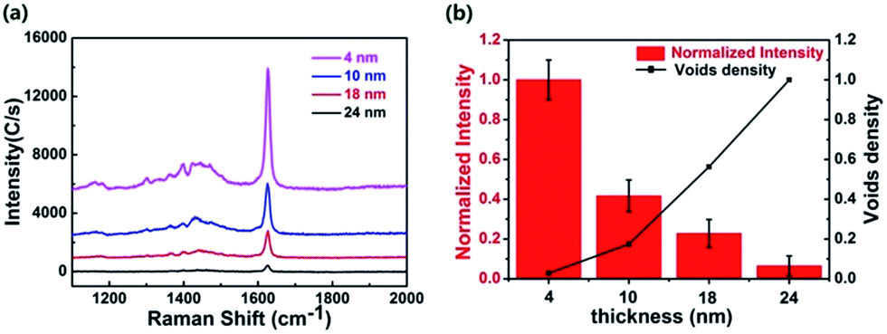 | ||
| Fig. 9 (a) SERS spectra of MB on MoO3@MIPs with shell thickness ranging from 4 to 24 nm. (b) Relation between the normalized peak intensity at 1625 cm−1 and shell thickness. The voids density in a fixed lens radius is approximately calculated based on shell thickness according to the same preparation process for the SERS substrate. | ||
4. Conclusions
In summary, we have successfully synthesized a novel MoO3@MIPs hybrid with a uniform and ultrathin shell (4 nm) through the pre-treating MoO3 with HNO3 and using MB as the model target. A selective SERS performance with a detection limit of 1.6 × 10⁴ was achieved and the SERS substrate can be photocatalytically recycled through a simple and effective “aim-and-shoot” way. The MIP-gating CT mechanism is proposed to illustrate the selective and sensitive SERS detection based on a series of control analyses on MoO3@MIPs with thicker shell but decreased sensitivity. We believe this “aim-and-shoot” strategy with excellent sensitivity, selectivity, and recyclability can greatly push forward the development of semiconductor-based SERS technology for complex detection.Conflict of interest
The authors declare no competing financial interest.Acknowledgements
This work has been supported by National Natural Science Foundation of China (21673073, U140710223 and 21377038), the National Basic Research Program of China (973 Program, 2013CB632403), the Science and Technology Commission of Shanghai Municipality (14230710500 and 16JC1401400), PetroChina Innovation Foundation 2015D-5006-0402, the Fundamental Research Funds for the Central Universities.References
- S. Nie and S. R. Emory, Science, 1997, 275, 1102–1106 CrossRef CAS PubMed.
- Z. Wang, S. Zong, W. Li, C. Wang, S. Xu, H. Chen and Y. Cui, J. Am. Chem. Soc., 2012, 134, 2993–3000 CrossRef CAS PubMed.
- D. Qi, X. Yan, L. Wang and J. Zhang, Chem. Commun., 2015, 51, 8813–8816 RSC.
- I. Alessandri and J. R. Lombardi, Chem. Rev., 2016, 116, 14921–14981 CrossRef CAS PubMed.
- W. Ren, Y. Fang and E. Wang, ACS Nano, 2011, 5, 6425–6433 CrossRef CAS PubMed.
- C. Y. Song, Y. J. Yang, B. Y. Yang, Y. Z. Sun, Y. P. Zhao and L. H. Wang, Nanoscale, 2016, 8, 17365–17373 RSC.
- J. Chenab, G. Qin, W. Shenb, Y. Lic and B. Das, J. Mater. Chem. C, 2015, 3, 1309–1318 RSC.
- P. P. Patra and G. V. P. Kumar, J. Phys. Chem. Lett., 2013, 4, 1167–1171 CrossRef CAS PubMed.
- M. P. Cecchini, V. A. Turek, J. Paget, A. A. Kornyshev and J. B. Edel, Nat. Mater., 2013, 12, 165–171 CrossRef CAS PubMed.
- S. M. Stranahan and K. A. Willets, Nano Lett., 2010, 10, 3777–3784 CrossRef CAS PubMed.
- E. C. Le Ru, M. Meyer and P. G. Etchegoin, J. Phys. Chem. B, 2006, 110, 1944–1948 CrossRef CAS PubMed.
- S. A. Piletsky, S. Alcock and A. P. F. Turner, Trends Biotechnol., 2001, 19, 9–12 CrossRef CAS PubMed.
- L. Chen, X. Wang, W. Lu, X. Wu and J. Li, Chem. Soc. Rev., 2016, 45, 2137–2211 RSC.
- Y. Hoshino, H. Koide, T. Urakami, H. Kanazawa, T. Kodama, N. Oku and K. J. Shea, J. Am. Chem. Soc., 2010, 132, 6644–6645 CrossRef CAS PubMed.
- E. Moczko, A. Poma, A. Guerreiro, I. P. de Vargas Sansalvador, S. Caygill, F. Canfarotta, M. J. Whitcombe and S. Piletsky, Nanoscale, 2013, 5, 3733–3741 RSC.
- M. Bompart, W. Y. De and K. Haupt, Adv. Mater., 2010, 22, 2343–2348 CrossRef CAS PubMed.
- E. L. Holthoff, D. N. Stratis-Cullum and M. E. Hankus, Sensors, 2011, 11, 2700–2714 CrossRef CAS PubMed.
- L. Chang, Y. Ding and X. Li, Biosens. Bioelectron., 2013, 50, 106–110 CrossRef CAS PubMed.
- Y. Lv, Y. Qin, F. Svec and T. Tan, Biosens. Bioelectron., 2016, 80, 433–441 CrossRef CAS PubMed.
- X. Wang, W. Shi, G. She and L. Mu, Phys. Chem. Chem. Phys., 2012, 14, 5891–5901 RSC.
- L. Bao, S. M. Mahurin and S. Dai, Anal. Chem., 2004, 76, 4531–4536 CrossRef CAS PubMed.
- H. Im, N. C. Lindquist, A. Lesuffleur and S. Oh, ACS Nano, 2010, 4, 947–954 CrossRef CAS PubMed.
- X. Zou, R. Silva, X. Huang, J. F. Al-Sharab and T. Asefa, Chem. Commun., 2013, 49, 382–384 RSC.
- G. Sinha, L. E. Depero and I. Alessandri, ACS Appl. Mater. Interfaces, 2011, 3, 2557–2563 CAS.
- T. Yang, W. Liu, L. Li, J. Chen, X. Hou and K. C. Chou, Nanoscale, 2017, 9, 2376–2384 RSC.
- X. Li, G. Chen, L. Yang, Z. Jin and J. Liu, Adv. Funct. Mater., 2010, 20, 2815–2824 CrossRef CAS.
- Z. Mao, W. Song, L. Chen, W. Ji, X. Xue, W. Ruan, Z. Li, H. Mao, S. Ma and J. R. Lombardi, J. Phys. Chem. C, 2011, 115, 18378–18383 CAS.
- D. Qi, L. Lu, L. Wang and J. Zhang, J. Am. Chem. Soc., 2014, 136, 9886–9889 CrossRef CAS PubMed.
- C. Qiu, Y. Bao, N. L. Netzer and C. Jiang, J. Mater. Chem. A, 2013, 1, 8790–8797 CAS.
- X. Tan, L. Wang, C. Cheng, X. Yan, B. Shen and J. Zhang, Chem. Commun., 2016, 52, 2893–2896 RSC.
- P. Zhang, Y. Wang, T. He, B. Zhang, X. Wang, H. Xin and F. Liu, Chem. Phys. Lett., 1988, 153, 215–222 CrossRef CAS.
- C. Muehlethaler, C. R. Considine, V. Menon, W. C. Lin, Y. H. Lee and J. R. Lombardi, ACS Photonics, 2016, 3, 1164–1169 CrossRef CAS.
- H. Wu, H. Wang and G. Li, Analyst, 2017, 142, 326–335 RSC.
- A. D. McFarland, M. A. Young, J. A. Dieringer and R. P. Van Duyne, J. Phys. Chem. B, 2005, 109, 11279–11285 CrossRef CAS PubMed.
- A. Musumeci, D. Gosztola, T. Schiller, N. M. Dimitrijevic, V. Mujica, D. Martin and T. Rajh, J. Am. Chem. Soc., 2009, 131, 6040–6041 CrossRef CAS PubMed.
- J. R. Lombardi and R. L. Birke, J. Phys. Chem. C, 2014, 118, 11120–11130 CAS.
- C. Boerigter, U. Aslam and S. Linic, ACS Nano, 2016, 10, 6108–6115 CrossRef CAS PubMed.
- L. Zhou, L. Yang, P. Yuan, J. Zou, Y. Wu and C. Yu, J. Phys. Chem. C, 2010, 114, 21868–21872 CAS.
- W. Li, D. Chen, F. Xia, J. Z. Tan, P. P. Huang, W. G. Song, M. N. Natalita and R. A. Caruso, Environ. Sci.: Nano, 2016, 3, 94–106 RSC.
Footnote |
| † Electronic supplementary information (ESI) available. See DOI: 10.1039/c7ra05547a |
| This journal is © The Royal Society of Chemistry 2017 |