 Open Access Article
Creative Commons Attribution 3.0 Unported Licence
A thermal-induced electric current from a gold electrode/porous silicon device†
Cheng-Yin Huang,
Chin-Kai Chang,
Kai-Shin Wen and
Vincent K. S. Hsiao *
*
Department of Applied Materials and Optoelectronic Engineering, National Chi Nan University, Nantou, Taiwan 54561. E-mail: kshsiao@ncnu.edu.tw
First published on 7th August 2017
Abstract
We demonstrate the electric current measured from a device composed of electrochemically etched silicon, porous silicon (PS) and gold (Au) electrodes of different device designs by applying a thermal potential between two Au electrodes. Compared to conventional PS of high contact resistance between Au/PS due to the homogeneously dispersed nanopores, our PS inhibits the discontinuous, island-shaped and micro-sized Si structures, which decrease the Au/PS contact resistance. When one Au electrode is heated, a temperature gradient (ΔT) is generated between the two electrodes and the electric current can be directly measured by a current meter under a close circuit condition. The output current not only depends on the electrode design but also on the distance between the electrodes. For the comb-shape electrode with finger lengths of 8 mm, widths of 0.1 mm, and finger separation of 0.14 mm, using a 25 °C setting temperature (Tset) can generate ΔT = 0.4 K, which corresponds to 14.2 μA. For the Au/PS device with two 16 mm2 square electrodes separated by a 2 mm distance, the current increases with increasing Tset and reaches a maximum value of 25 μA corresponding to ΔT = 3.4 K. Our Au/PS device has potential in sensitive temperature sensors operated at temperatures lower than 60 °C.
Introduction
Nanostructured silicon (n-Si) with cost-effective properties, which can be easily integrated into CMOS processing, has been considered as the ultimate thermoelectric material.1–3 Several studies have theoretically or experimentally demonstrated the enhanced thermoelectric power of n-Si from the evaluation of the Seebeck coefficient S (S = ΔV/ΔT, where ΔV and ΔT are the potential and temperature gradient between the electrode from the thermoelectric device, respectively) and figures of merit ZT (ref. 4–20) (ZT = σS2T/κ, where σ and κ are the electrical and thermal conductivity of the material, respectively and T is the absolute temperature) due to the decrease of κ from n-Si when compared to bulk Si. Nassiopoulou et al., constructed a thermoelectric device with an output thermoelectric power of 0.4 μW cm−2 using porous Si (PS) as a thermal isolator21 and demonstrated the porosity-dependent Seebeck coefficient from PS20 (1 mV K−1 for a 50% porosity PS). Fischer et al., experimentally characterized the thermoelectric properties of nanoporous Si nanowires with a Seebeck coefficient of 1.2 mV K−1.22 Conventional evaluation of the Seebeck coefficient involves generating a temperature gradient (ΔT) and measuring the potential difference (ΔV) under an open circuit condition. In this study, we heated a gold (Au) electrode/PS junction and measured the electric current between the hot and cold junction under a close circuit condition, as shown in Fig. 1. Since the Peltier effect is described as a heating or cooling effect, which can be induced by applying currents between two electrodes connected with a thermoelectric material only under a closed circuit condition, we demonstrated a reversed Peltier effect or unconventional Seebeck effect where the generated electric current at the Au/PS junction was proportional to the heat absorbed from the device. Our experimental results show that by heating one Au/PS junction, an electric current can be directly measured using a current meter. For an Au/PS thermoelectric device with a comb-shape electrode with finger electrodes separated at a short distance (0.14 mm), a 0.4 K temperature gradient generated a 14 μA electric current. Different electrochemical etching conditions and electrode design provide different electric current behavior. Other devices, such as using square electrodes of 16 mm2 with at least 1 mm separation between the two electrodes, exhibited higher ΔT values under the same heating conditions (Tset) controlled by a flexible heater. For an Au/PS thermoelectric device with square electrodes separated by 2 mm, a 25 μA electric current was obtained by generating ΔT = 3.4 K at Tset = 70 °C.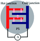 | ||
| Fig. 1 A schematic of the current measurement from an Au electrode/PS junction device under close circuit conditions by heating one side of the Au electrode. | ||
Experimental
PS samples were prepared at room temperature via a wet electrochemical etching process in hydrofluoric acid (HF) using p-type boron doped single crystalline Si (with a thickness of approximately 500 μm and resistivity of 1–10 Ω cm) in (100) orientation. Electrochemical etching was performed in a home-made Teflon cell at a constant current density of 30 mA cm−2 for 30, 40 and 50 min in an electrolyte solution of 48 wt% HF, 98 wt% isopropanol (IPA), and deionized (DI) water. The electrolyte consisted of a HF![[thin space (1/6-em)]](https://www.rsc.org/images/entities/char_2009.gif) :
:![[thin space (1/6-em)]](https://www.rsc.org/images/entities/char_2009.gif) IPA
IPA![[thin space (1/6-em)]](https://www.rsc.org/images/entities/char_2009.gif) :
:![[thin space (1/6-em)]](https://www.rsc.org/images/entities/char_2009.gif) DI water solution with a volume ratio of 1
DI water solution with a volume ratio of 1![[thin space (1/6-em)]](https://www.rsc.org/images/entities/char_2009.gif) :
:![[thin space (1/6-em)]](https://www.rsc.org/images/entities/char_2009.gif) 2
2![[thin space (1/6-em)]](https://www.rsc.org/images/entities/char_2009.gif) :
:![[thin space (1/6-em)]](https://www.rsc.org/images/entities/char_2009.gif) 1. The control experiment for the PS sample was fabricated using an electrolyte composed of HF
1. The control experiment for the PS sample was fabricated using an electrolyte composed of HF![[thin space (1/6-em)]](https://www.rsc.org/images/entities/char_2009.gif) :
:![[thin space (1/6-em)]](https://www.rsc.org/images/entities/char_2009.gif) ethanol = 1
ethanol = 1![[thin space (1/6-em)]](https://www.rsc.org/images/entities/char_2009.gif) :
:![[thin space (1/6-em)]](https://www.rsc.org/images/entities/char_2009.gif) 1 (volume ratio). For each sample, the Au electrode was directly deposited onto the PS using a thermal evaporation method with a shadow mask. For the electric current measurements, an ultra-thin flexible heater (KLC Corporation, Taiwan) was attached to the backside of the PS sample and a current meter (Keithley 6485 picoamp meter with 10 fA resolution) was directly connected to the two electrodes, as shown in Fig. S1a and b.† The heating conditions (Tset) were controlled by setting the temperature of the heater. The current was directly recorded from the current meter under close circuit conditions without applying an external voltage. The positive (negative) value of the current was obtained by heating the Au electrode connected to the negative (positive) probe of the current meter. The ΔT between electrodes was measured using a thermal IR detector.
1 (volume ratio). For each sample, the Au electrode was directly deposited onto the PS using a thermal evaporation method with a shadow mask. For the electric current measurements, an ultra-thin flexible heater (KLC Corporation, Taiwan) was attached to the backside of the PS sample and a current meter (Keithley 6485 picoamp meter with 10 fA resolution) was directly connected to the two electrodes, as shown in Fig. S1a and b.† The heating conditions (Tset) were controlled by setting the temperature of the heater. The current was directly recorded from the current meter under close circuit conditions without applying an external voltage. The positive (negative) value of the current was obtained by heating the Au electrode connected to the negative (positive) probe of the current meter. The ΔT between electrodes was measured using a thermal IR detector.
Results and discussion
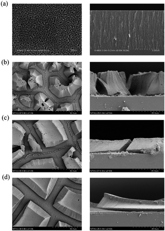
Fig. 2 shows the surface and cross-sectional scanning electron microscopy (SEM) images of the electrochemically etched PS. A typical use of ethanol, along with HF for anodized etching of PS, is to eliminate hydrogen bubbles, making the etching process more homogeneous and generating well-dispersed nanopores inside the PS layer, as shown in Fig. 2a. However, the use of IPA facilitates inhomogeneous etching23 and a discontinuous, micro-size and island-shape PS layer is obtained, as shown in Fig. 2b. The observed island-like shapes in the PS samples play critical roles in the photothermoelectric effect reported previously.24 The increased island-shaped areas and decreased etching thicknesses were observed in the PS samples as the etching time increased, as shown in Fig. 2c and d. Table 1 shows the measured electric current obtained from the Au/PS junction devices with comb-shape electrode design (finger separation of 0.14 mm) using PS fabricated under different etching conditions with the same electrode heating conditions (Tset = 25 °C). For the Au/PS device using PS fabricated by conventional etching without using IPA, no evident electric current was observed; however, an enhanced electric current (14 μA) was observed from the PS samples fabricated using IPA. The Seebeck coefficient of PS fabricated from a conventional recipe of mixed HF/ethanol was 0.6–1.0 μV K−1 measured in the temperature range 150–300 K.5,20 The electrical conductivity of PS was measured to be 5–10 Ω−1 cm−1 in the same temperature range.5 Therefore, the calculated current from the comb-shape electrode Au/PS device, in which the PS was fabricated without using IPA, was 1 nA, which is close to our measured current, as shown in Table 1. The enhanced electric current measured from the Au/PS device consisted of discontinuous, island-shape and micro-size PS may due to the decrease of contact resistance between the Au electrode and PS and the leakage current inside the PS. A previous study on the linear I–V characteristics24 proved the concept of low contact resistance and the leakage current of the device. The measured current decreased upon increasing the etching time, which may be attributed to a decrease in the thickness of the micro-sized PS layers. In addition, the amount of nanopores reduced on increasing the etching time whose effect prevented the quantum confinement of PS and further reduced the electrical conductivity inside PS. Therefore, the thermal-induced electrical current decreased with an increased etching time.| Sample preparation conditions | TEC (μA) |
|---|---|
HF![[thin space (1/6-em)]](https://www.rsc.org/images/entities/char_2009.gif) : :![[thin space (1/6-em)]](https://www.rsc.org/images/entities/char_2009.gif) ethanol = 1 ethanol = 1![[thin space (1/6-em)]](https://www.rsc.org/images/entities/char_2009.gif) : :![[thin space (1/6-em)]](https://www.rsc.org/images/entities/char_2009.gif) 1 1 |
+0.004/−0.004 |
HF![[thin space (1/6-em)]](https://www.rsc.org/images/entities/char_2009.gif) : :![[thin space (1/6-em)]](https://www.rsc.org/images/entities/char_2009.gif) IPA IPA![[thin space (1/6-em)]](https://www.rsc.org/images/entities/char_2009.gif) : :![[thin space (1/6-em)]](https://www.rsc.org/images/entities/char_2009.gif) DI water = 1 DI water = 1![[thin space (1/6-em)]](https://www.rsc.org/images/entities/char_2009.gif) : :![[thin space (1/6-em)]](https://www.rsc.org/images/entities/char_2009.gif) 2 2![[thin space (1/6-em)]](https://www.rsc.org/images/entities/char_2009.gif) : :![[thin space (1/6-em)]](https://www.rsc.org/images/entities/char_2009.gif) 1/etching 30 min 1/etching 30 min |
+14.2/−10.9 |
HF![[thin space (1/6-em)]](https://www.rsc.org/images/entities/char_2009.gif) : :![[thin space (1/6-em)]](https://www.rsc.org/images/entities/char_2009.gif) IPA IPA![[thin space (1/6-em)]](https://www.rsc.org/images/entities/char_2009.gif) : :![[thin space (1/6-em)]](https://www.rsc.org/images/entities/char_2009.gif) DI water = 1 DI water = 1![[thin space (1/6-em)]](https://www.rsc.org/images/entities/char_2009.gif) : :![[thin space (1/6-em)]](https://www.rsc.org/images/entities/char_2009.gif) 2 2![[thin space (1/6-em)]](https://www.rsc.org/images/entities/char_2009.gif) : :![[thin space (1/6-em)]](https://www.rsc.org/images/entities/char_2009.gif) 1/etching 40 min 1/etching 40 min |
+12.2/−11.3 |
HF![[thin space (1/6-em)]](https://www.rsc.org/images/entities/char_2009.gif) : :![[thin space (1/6-em)]](https://www.rsc.org/images/entities/char_2009.gif) IPA IPA![[thin space (1/6-em)]](https://www.rsc.org/images/entities/char_2009.gif) : :![[thin space (1/6-em)]](https://www.rsc.org/images/entities/char_2009.gif) DI water = 1 DI water = 1![[thin space (1/6-em)]](https://www.rsc.org/images/entities/char_2009.gif) : :![[thin space (1/6-em)]](https://www.rsc.org/images/entities/char_2009.gif) 2 2![[thin space (1/6-em)]](https://www.rsc.org/images/entities/char_2009.gif) : :![[thin space (1/6-em)]](https://www.rsc.org/images/entities/char_2009.gif) 1/etching 50 min 1/etching 50 min |
+5.9/−5.2 |
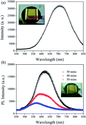
The peak intensity of the photoluminescence (PL) was observed from the PS samples etched without using IPA at 720 nm, as shown in Fig. 3a, in addition, no evident electric current was observed from that etched sample upon generating a heat potential at the two gold electrodes. The peak intensity of the PL observed from PS etched using IPA was blue-shifted to 630 nm, as shown in Fig. 3b. The blue-shifted PL may be attributed to the change in the surface morphology of the PS samples fabricated using IPA, as shown in Fig. 2. The PL intensity decreased as the electrochemical etching time increased. The measured electric current from the PS samples under the same heating conditions also decreased as the etching time increased. Previous studies5,6 have shown that the PL and the Seebeck coefficient are affected by the porosity of PS. The Seebeck coefficient increased with increasing porosity, reached a maximal value at 51% porosity and then decreased.20 However, no PL peak was observed from the samples of 51% porosity.20 Herein, we observed that the maximal electric current was obtained from a sample etched for 30 min with the highest PL intensity. The PL peak wavelength was blue-shifted with an increased etching time, indicating a decrease in the crystal size of the nanocrystalline Si. Therefore, the porosity increased with increased etching time because of the decrease in the crystal size of the nanocrystalline Si. The increased porosity helped to increase the thermal conductivity value; however, the electrical conductivity decreased with increasing porosity. More investigation must be carried out to examine the dependence of the Seebeck coefficient on the surface morphology using an Au/PS simple design where the PS can be fabricated under different etching conditions, such as composition of electrolyte and etching current density.
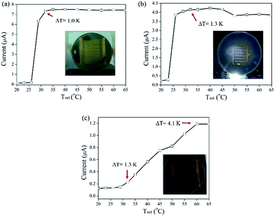
Fig. 4 shows the Tset-dependent current measured from an Au/PS device using different electrode designs. Tset represents the temperature setting in the flexible heater attached on the bottom of the Au/PS device. The electric current suddenly increases as the setting temperature becomes larger than 26 °C, as shown in Fig. 4a. The temperature gradient (ΔT) between the two Au gold electrodes remains unchanged even upon increasing the heating temperature due to the small separation distance (0.14 mm) between the fingers. A larger finger separation (0.6 mm) helps increase the ΔT value, as shown in Fig. 4b; however, the measured electric current between the two electrodes also decreases. Using the electrode design without the use of fingers, as shown in Fig. 5b (inset), a high ΔT value was generated, but the generated electric current was comparably lower than that of the device with finger electrodes, as shown in Fig. 4c.
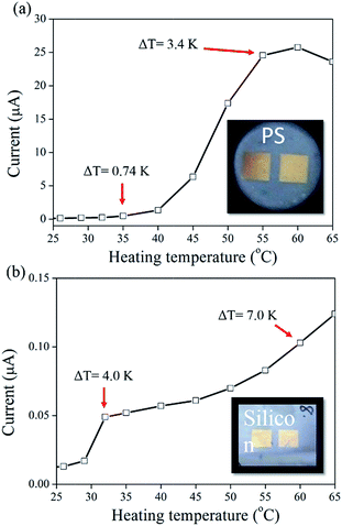
To verify the electrode separation-dependent current, a more simple design of the Au/PS devices were fabricated and measured. Two 4 mm × 4 mm square electrodes separated by different distances were used in the Au/PS devices, as shown in Fig. 5a (inset). When the Au electrode, which was connected to the current meter with the negative probe, was heated, a positive electric current was obtained due to the generation of ΔT between the two electrodes. The current increased with increasing heating temperature, which generated a larger ΔT value. The current reached a maximum value of 25 μA corresponding to ΔT = 3.4 K, as shown in Fig. 5a. A control sample comprising a Au/single-crystalline Si device was fabricated and measured under different heating temperatures and no evident thermal current was observed (0.10 μA) when Tset = 60 °C, corresponding to ΔT = 7 K, as shown in Fig. 5b.
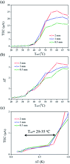
Fig. 6 shows the thermal current behaviour of the Au/PS devices with different distance between the two Au electrodes. When the setting conditions were in the range of 52–60 °C, a 2 mm separation Au/PS device had a larger thermal-induced electric current than the other devices with different electrode separation distances. The current slightly decreased or remained unchanged when the heating temperature was higher than 60 °C, as shown in Fig. 6a. A ΔT between the two electrodes was measured and the heating temperature-dependent ΔT was characterized in different devices, as shown in Fig. 6b. It is of interest that the separation between the two electrodes provided different ΔT value under the same setting temperature conditions. When the samples were measured at higher setting temperature (Tset > 60 °C), the same Tset provided higher values of ΔT in the 2 mm separation Au/PS devices, which also showed higher values for the thermal-induced current. At a moderate setting temperature range (Tset = 52–60 °C), a 1 mm separation Au/PS device showed a larger ΔT, which corresponds to the maximal current. At a low setting temperature range (Tset = 29–35 °C), a 0.5 mm separation Au/PS device had a large ΔT value and thermal-induced current, as shown in Fig. 6c.
Conclusions
We measured the TECs generated from simple thermoelectric devices composed of Au/PS. When one electrode was heated, a thermal potential corresponding to a TEC was generated and measured in a close circuit connection. The TECs were characterized from the PS samples fabricated under different electrochemical etching conditions. A 30 min etched PS sample with the highest PL intensity and relatively thick etching thickness showed better TEC performance. Different electrode designs affected the performance levels of the Au/PS thermoelectric devices. Our demonstration is suitable for highly sensitive sensors intended for operation at low temperatures or photovoltaic–thermoelectric hybrid devices.Acknowledgements
This study was funded by the Ministry of Science and Technology (MOST), Taiwan, under project number MOST-103-2221-E-260-016-MY3.Notes and references
- R. Venkatasubramanian, E. Siivola, T. Colpitts and B. O'Quinn, Nature, 2001, 413, 597 CrossRef CAS PubMed.
- A. I. Boukai, Y. Bunimovich, J. Tahir-Kheli, J. K. Yu, W. A. Goddard III and J. R. Heath, Nature, 2008, 451, 168 CrossRef CAS PubMed.
- A. I. Hochbaum, R. Chen, R. D. Delgado, W. Liang, E. C. Garnett, M. Najarian, A. Majumdar and P. Yang, Nature, 2008, 451, 163 CrossRef CAS PubMed.
- J. L. G. Gesele, V. Drach, J. Fricke and R. Arens-Fischer, J. Phys. D: Appl. Phys., 1997, 30, 2911–2916 CrossRef.
- R. G. Mathur, R. M. Mehra and P. C. Mathur, J. Appl. Phys., 1998, 83, 5855 CrossRef CAS.
- A. Yamamoto, H. Takazawa and T. Ohta, 18th International Conference on Thermoelectrics, 1999, p. 428 Search PubMed.
- D. Kraemer, L. Hu, A. Muto, X. Chen, G. Chen and M. Chiesa, Appl. Phys. Lett., 2008, 92, 243503 CrossRef.
- J. H. Lee, G. A. Galli and J. C. Grossman, Nano Lett., 2008, 8, 3750 CrossRef CAS PubMed.
- F. X. Alvarez, D. Jou and A. Sellitto, Appl. Phys. Lett., 2010, 97, 033103 CrossRef.
- J. Tang, H. T. Wang, D. H. Lee, M. Fardy, Z. Huo, T. P. Russell and P. Yang, Nano Lett., 2010, 10, 4279 CrossRef CAS PubMed.
- N. Wang, L. Han, H. He, N.-H. Park and K. Koumoto, Energy Environ. Sci., 2011, 4, 3676 CAS.
- D. D. Y. He, J.-H. Lee, J. C. Grossman and G. Galli, ACS Nano, 2011, 5, 1839 CrossRef PubMed.
- Z.-G. Chen, G. Han, L. Yang, L. Cheng and J. Zou, Prog. Nat. Sci.: Mater. Int., 2012, 22, 535 CrossRef.
- N. Neophytou, X. Zianni, H. Kosina, S. Frabboni, B. Lorenzi and D. Narducci, Nanotechnology, 2013, 24, 205402 CrossRef PubMed.
- K. T. Park, S. M. Shin, A. S. Tazebay, H. D. Um, J. Y. Jung, S. W. Jee, M. W. Oh, S. D. Park, B. Yoo, C. Yu and J. H. Lee, Sci. Rep., 2013, 3, 2123 CrossRef PubMed.
- G. H. Tang, C. Bi and B. Fu, J. Appl. Phys., 2013, 114, 184302 CrossRef.
- G. Pennelli, Beilstein J. Nanotechnol., 2014, 5, 1268 CrossRef PubMed.
- G. Schierning, Phys. Status Solidi A, 2014, 211, 1235–1249 CrossRef CAS.
- M. J. Lee, J. H. Ahn, J. H. Sung, H. Heo, S. G. Jeon, W. Lee, J. Y. Song, K. H. Hong, B. Choi, S. H. Lee and M. H. Jo, Nat. Commun., 2016, 7, 12011 CrossRef CAS PubMed.
- K. Valalaki, P. Benech and A. Galiouna Nassiopoulou, Nanoscale Res. Lett., 2016, 11, 201 CrossRef PubMed.
- E. Hourdakis and A. G. Nassiopoulou, Sensors, 2013, 13, 13596 CrossRef CAS PubMed.
- G. Yuan, R. Mitdank, A. Mogilatenko and S. F. Fischer, J. Phys. Chem. C, 2012, 116, 13767 CAS.
- H. Kim and N. Cho, Nanoscale Res. Lett., 2013, 7, 408 CrossRef PubMed.
- Y.-S. Lai, C.-Y. Tsai, C.-K. Chang, C.-Y. Huang, V. K. S. Hsiao and Y. O. Su, Adv. Mater., 2016, 28, 2644 CrossRef CAS PubMed.
Footnote |
| † Electronic supplementary information (ESI) available. See DOI: 10.1039/c7ra05474b |
| This journal is © The Royal Society of Chemistry 2017 |

