
 Open Access Article
 This Open Access Article is licensed under a
 Creative Commons Attribution 3.0 Unported Licence
Unusual renormalization group (RG) flow and temperature-dependent phase transition in strongly-insulating monolayer epitaxial graphene†
Lung-I. Huangab,
Yanfei Yangac,
Chieh-Wen Liuad,
Randolph E. Elmquist a,
Shun-Tsung Lo*d,
Fan-Hung Liud and
Chi-Te Liang*bde
a,
Shun-Tsung Lo*d,
Fan-Hung Liud and
Chi-Te Liang*bde
aNational Institute of Standards and Technology (NIST), Gaithersburg, MD 20899, USA. E-mail: shuntsunglo@mail.ncku.edu.tw
bDepartment of Physics, National Taiwan University, Taipei 106, Taiwan. E-mail: ctliang@phys.ntu.edu.tw
cJoint Quantum Institute, University of Maryland, College Park, MD 20742, USA
dGraduate Institute of Applied Physics, National Taiwan University, Taipei 106, Taiwan
eDepartment of Physics, Stanford University, Stanford, CA 94305, USA
First published on 19th June 2017
Abstract
By changing the measurement temperature (T), one can vary the effective sample size so as to study the renormalization group (RG) (or T-driven) flow of a semiconductor, a topological insulator, or a graphene device in the complex conductivity plane. Here we report RG flow of large-area, strongly disordered monolayer graphene epitaxially grown on SiC, which becomes insulating as T decreases for zero magnetic field. We observe cusp-like RG flow towards (σxy = e2/h, σxx = e2/h) where σxy and σxx are Hall conductivity and diagonal conductivity respectively. Such features, indicative of a fixed-temperature phase transition, have never been observed before and cannot be explained by existing RG models based on a modular symmetry group. Therefore, our results suggest the need for new theoretical models and experimental study leading to an understanding of strongly disordered two-dimensional materials such as graphene, few-layer black phosphorus, WSe2, and so on.
Introduction
Graphene, which is a single layer of carbon atoms bonded in a honeycomb lattice,1,2 has continued to attract worldwide interest. Graphene prepared by mechanical exfoliation3 is of ultra-high quality and thus allows one to probe fascinating physical phenomena such as the Berry phase,1,2 anomalous integer quantum Hall effects,1,2 fractional quantum Hall effects,4–7 imaging cyclotron orbits,8 and so on. However, its limited size may not be suitable for maintaining the quantum Hall resistance (QHR) standard, which provides the unit of resistance in the International System (SI), or for large-scale integration of electronic devices. In contrast, monolayer graphene epitaxially grown on SiC,9 which can be of wafer-size and most importantly does not require any transfer process, is now widely believed to be an ideal candidate for replacing existing GaAs-based QHR reference standards.10–16 In addition, recently it has been shown that monolayer epitaxial graphene grown on SiC is an interesting platform for studying the insulator-relativistic quantum Hall transition in graphene,17,18 insulating behavior,17–19 variable range hopping,19 and so forth. Such measurements may well reveal the true ground-state of disordered graphene and shed light on possible band-gap opening in graphene on SiC.20Pioneering work shows that by changing the measurement temperature T, one can effectively vary the size of a sample and study the temperature-driven (renormalization group (RG)) flow of the device.21,22 Such a RG flow diagram is extremely useful for understanding the quantum Hall (QH) effect and the QH plateau–plateau transition (normally based on the semicircle law21–25) which is a quantum phase transition. Let us consider the simplest case. For a system with a single conduction channel the semicircle represents a critical boundary for the ν = 2 QH state, with a stable point on the x-axis at (σxy, σxx) = (2e2/h, 0). An unstable point18 at (σxy = e2/h, σxx = e2/h) represents the boundary between two types of RG flow. To the left of the unstable point, the RG flows are towards (σxy = 0, σxx = 0) which is the insulating state. To the right of the unstable point, the RG flows are towards (σxy = 2e2/h, σxx = 0), which is the ν = 2 QH state (Fig. 1).
 | ||
| Fig. 1 Schematic diagram showing RG flow in the conductivity plane. The red dot corresponds to the unstable point. The red arrows indicate the directions of the RG flow. | ||
RG flow lines in disordered two-dimensional (2D) systems are understood by referring to the semicircle law with a clear unstable point. Such results provide important information on the insulating behaviour in monolayer epitaxial graphene grown on SiC17–19 and the transition17,18 at low fields between an insulator and the ν = 2 QH state, which cannot be seen in many other graphene-like systems. For example, in our previous work, RG flow approximated by the semicircle law is only observed in the strongest disorder device even if clear crossing points in the longitudinal resistivity ρxx are observed in all three monolayer graphene devices grown on SiC.18 Such results suggest that the unique insulator-relativistic QH transition in disordered graphene17 is better studied by the RG flows rather than by the crossing point in ρxx since RG flows described by the semicircle law strongly point to the floating-up of the N = 0 Landau level at low magnetic fields. Moreover, the unstable fixed point in the RG flows unequivocally shows signature of a quantum phase transition. In order to further probe the RG flow in graphene and possibly new physical phenomena related to the unique relativistic ν = 2 QH state, we measure a disordered graphene device on SiC that is strongly insulating in the sense that the magneto-resistance decreases with increasing temperature (T ≤ 100 K) over a wide range of temperature and magnetic field. Such a device is more disordered compared with those studied17,18 in the sense that the zero-field resistivity is well above the quantum resistance h/e2. Interestingly, we observe cusp-like RG flow towards (σxy = e2/h, σxx = e2/h) which cannot be explained by existing RG models mostly based on the modular symmetry group. Our new experimental results suggest a fixed-temperature phase transition instead of a magnetic-field-induced quantum phase transition in strongly insulating graphene. We suggest that further theoretical and experimental work is required for understanding this hitherto unexplored research area.
Results and discussion
Fig. 2 shows the longitudinal and Hall resistivities of the device at different temperatures. At T = 15 K, the carrier density and mobility of the device are calculated to be 9 × 1010 cm−2 and 830 cm2 V−1 s−1. At T < 15 K, strongly insulating behaviour in makes the symmetrized ρxx and ρxy unreliable therefore we concentrate on data for T ≥ 15 K. At zero magnetic field, the sample behaves as an insulator in the sense that ρxx always decreases with increasing temperature.26 For T ≤ 100 K, ρxx(B) decreases with increasing T over a wide range of B (≤4.5 T).27
 | ||
| Fig. 2 Longitudinal and Hall resistivities (ρxx and ρxy) at various temperatures T, with temperature denoted by the color of the line. | ||
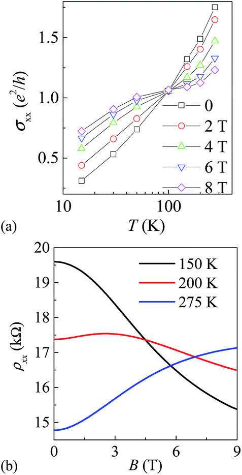
Fig. 3(a) and (b) show the converted σxx and σxy at different temperatures. Here, the insulating nature of the device is clearly observed from the increase in σxx with T for all values of B studied, while σxy displays maximal values at T ≈ 100 K for all B. The diagonal conductivity σxx is almost magnetic-field-independent for T ≈ 100–150 K. Such an observed temperature dependence shows that even though signs of a quantum Hall-like step close to h/(2e2) in ρxy are seen at low temperature, we do not have a true ν = 2 QH state. A possible reason is that the disorder within the sample is so strong that the QH state is destroyed. That σxy does not show quantized plateau values close to 2e2/h is due in part to large ρxx in the high-field regime (Fig. 3(b)). Such results again suggest that the device does not enter the ν = 2 QH state.
 | ||
| Fig. 3 (a) σxx (b) σxy as a function of B at various T. The line colors correspond to temperatures as given in Fig. 2. | ||
We next develop the RG flow diagram of (σxy, σxx) as shown by superimposed arrows pointing in the direction of the lowest T at a series of fixed B (Fig. 4(a) and (b)). For low B the T-driven flow forms a set of curves that converge toward the insulating state at (0,0). Such results strongly demonstrate that the device behaves as an insulator. Empirically, we observe quadratic decrease in ρxx(B) and linear rise in ρxy(B) over a wide temperature range for B < 0.3 T, where the flow curves follow nearly straight paths along the σxx axis. The quadratic negative MR is indicative of strong localization of carriers.28 For B > 0.3 T, the curves for fixed B bend outward in the range near σxx = e2/h and at higher B a cusp appears near the unstable point at (e2/h, e2/h). We wish to point out that such cusp-like RG flow cannot be observed in a similar GaAs-based disordered electron system in which the device is in the insulating regime with a ν = 2 QH-like plateau structure (ESI Fig. 2†). Such results strongly suggest that the cusp-like RG flow is a unique feature in strongly disordered graphene.
 | ||
| Fig. 4 (a) Conductivity σxx plotted against σxy EG4. The dotted curves denote the theoretical prediction of semicircle σxy − σxx relation for the 0–2 transition. Each group of triangle markers connected by dashed lines denotes the data for the same magnetic field (B = 3 T). The arrows indicate the flow line to the low temperature extreme at fixed magnetic fields. (b) Detailed RG flow over a wide range of T. | ||
Quantum phase transitions (QPTs) in the QH regime may lie between adjacent QH states or separate the QH state from insulating states at either low or high perpendicular B fields in two dimensions.29–32 The cusp in RG flow does not resemble a QPT, but rather suggests a fixed-temperature phase transition, as shown in Fig. 5(a), with a field-independent crossing at σxx ≈ e2/h. This high-disorder state displays features of the ν = 2 QH state by approaching ρxy ≈ h/(2e2) at high fields and low T. Meanwhile, σxx ≈ e2/h near the field-independent crossing and continues to rise smoothly as T increases, resulting in the crossover from positive to negative slope of the diagonal magneto-conductivity vs. T as shown in Fig. 4(a). To further illustrate this interesting behavior, we expand the plot of ρxx(B) at high T in Fig. 5(b) and find that there is a crossover from negative to positive MR with increasing T. Jabakhanji et al.33 observed positive magnetoresistance (MR) in highly doped graphene grown by chemical vapor deposition on SiC and argued that it is due to the energy dependence of mobility that is prominent at high T. This dependence may result from scattering by ionized impurities or by phonons produced at the graphene/SiC interface. In their work at low T the T-independent crossing point in ρxx (superimposed on the background parabolic negative MR) was observed when the product of mobility and magnetic field is equal to 1 and is presumably due to electron–electron interaction corrections. Moreover, with increasing B above the T-independent crossing point, Landau quantization gave rise to Shubnikov-de Haas (SdH) oscillations in ρxx. In our experiments, the sample shows neither SdH oscillations nor the well-developed QH effect, probably due to stronger disorder within this graphene device. The crossover from negative MR to positive MR may be due to strong electron-phonon scattering which increases the high-field MR.
 | ||
| Fig. 5 (a) Temperature dependence of the diagonal conductivity for device EG4 in the range 15 K ≤ T ≤ 275 K. The crossing point occurs at T = (97 ± 1) K. (b) ρxx(B) in the high-T regime. | ||
In conclusion, we observe an insulating state that persists at all fields studied and coexists with weak QH-like characteristics at moderate and higher field strength. For T < 100 K, σxx shows monotonic decrease with increasing B. In contrast, For T > 100 K σxx increases with increasing B, and for T ≈ 100 K it passes through a field-independent crossing. In the low field insulating regime, carriers are localized as a result of the presence of strong disorder, and display quadratic negative MR. At higher B a cusp appears near the unstable point at (e2/h, e2/h) in the RG flow diagram. A possible reason is that the ν = 2 QH state in graphene on SiC is very robust so that even strong disorder and high ρxx within the device can co-exist with the presence of a QH-plateau-like structure in ρxy. We speculate that this may lead to the observed cusp-like RG flow towards (σxy = e2/h, σxx = e2/h). However, as our new results cannot be explained by any existing RG models based on the modular symmetry group, further experimental and theoretical studies are needed in order to probe this hitherto unexplored interesting area in the field of disordered 2D materials.34
Experimental
Materials preparation
During the high-temperature annealing process near T = 1900 °C, Si atoms sublimate and C atoms reorganize into graphene layers while the SiC(0001) substrate forms atomically-flat terraces. The initial graphene layer lies on top of and across the terraces, forming a (6√3 × 6√3)R30° reconstruction on the Si face that is azimuthally oriented to the SiC lattice.35 This zero-layer graphene is covalently bonded to Si atoms in the substrate and is non-conducting. It is often described as the buffer layer on the Si-face SiC(0001) surface because of its effect on the carrier concentration in conducting graphene layers. Conducting epitaxial graphene is created as additional carbon forms a new buffer layer interface beneath an electrically-active monolayer of graphene.36Device fabrication
Hall bar devices of width w = 100 μm and length l = 600 μm were fabricated on monolayer epitaxial graphene samples using a clean lithographic technique.36 Throughout the lithography the conducting epitaxial graphene channels were isolated from chemical residues by a protective layer of precious metal, which was removed using dilute aqua regia (DAR) at the last processing step. The DAR completely dissolves the protective precious metal layer as shown by energy-dispersive X-ray spectroscopy and X-ray photoelectron spectroscopy. While as-grown epitaxial graphene typically is heavily electron doped (n ≈ 1013 cm−2), the device used in this study has low carrier concentration n ≈ 1011 cm−2.37 Residual molecular transfer doping brings the carrier concentration close to the Dirac point, while n-type carrier concentrations above n ≈ 5×1012 cm−2 can be readily restored non-destructively36 by heating the sample at T ≥ 125 °C in vacuum. The RG flow characteristics of several less-disordered devices prepared similarly have been discussed in an earlier publication.18Characterization
In graphene, low carrier concentrations are often associated with electron–hole puddles38,39 and this spatially correlated disorder leads to percolating current paths38 which convolve with slight misalignment of the voltage contacts to mix ρxx with ρxy. In order to circumvent the mixing of resistivity components we symmetrize the resistivity40 as ρxx(B) = [ (B) +
(B) +  (−B)]/2 and ρxy(B) = [
 (B) −
(B) −  (−B)]/2. The diagonal resistivity
 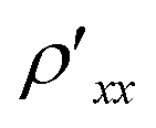 = (V13 + V1*3*)/(2ISD) was measured between the two outer sets of voltage contacts (V13 and V1*3*), and the off-diagonal resistivity
  was measured as the Hall resistance Rxy = V22*/ISD across the device at the middle set of voltage contacts (V22*) (ESI Fig. 1†). All of the transport data were recorded using low-frequency lock-in measurements at source-drain current ISD below 1 μA. Magnetic field levels up to ±9 T were applied perpendicular to the sample surface41,42 and the field was swept in the negative direction at a rate of 0.022 T s−1.
Acknowledgements
We would like to thank the Ministry of Science and Technology (MOST), Taiwan for support (grant no. MOST 105-2119-M-002-048-MY3).References
- K. S. Novoselov, A. K. Geim, S. V. Morozov, D. Jiang, M. I. Katsnelson, I. V. Grigorieva, S. V. Dubonos and A. A. Firsov, Nature, 2005, 438, 197–200 CrossRef CAS PubMed.
- Y. Zhang, Y.-W. Tan, H. L. Stormer and P. Kim, Nature, 2005, 438, 201–204 CrossRef CAS PubMed.
- K. S. Novoselov, A. K. Geim, S. V. Morozov, D. Jiang, Y. Zhang, S. V. Dubonos, I. V. Grigorieva and A. A. Firsov, Science, 2004, 306, 666–669 CrossRef CAS PubMed.
- K. I. Bolotin, F. Ghahari, M. D. Shulman, H. L. Stormer and P. Kim, Nature, 2009, 462, 196–199 CrossRef CAS PubMed.
- X. Du, I. Skachko, F. Duerr, A. Luican and E. Y. Andrei, Nature, 2009, 462, 192–195 CrossRef CAS PubMed.
- C. R. Dean, A. F. Young, P. Cadden-Zimansky, L. Wang, H. Ren, K. Watanabe, T. Taniguchi, P. Kim, J. Hone and K. L. Shepard, Nat. Phys., 2011, 7, 693–696 CrossRef CAS.
- B. Feldman, B. Krauss, J. H. Smet and A. Yacoby, Science, 2012, 337, 1196–1199 CrossRef CAS PubMed.
- S. Bhandari, G.-H. Lee, A. Klales, K. Watanabe, T. Taniguchi, E. Heller, P. Kim and R. M. Westervelt, Nano Lett., 2016, 16, 1690–1694 CrossRef CAS PubMed.
- C. Berger, Z. Song, T. Li, X. Li, A. Y. Ogbazghi, R. Feng, Z. Dai, A. N. Marchenkov, E. H. Conrad, P. N. First and W. A. de Heer, J. Phys. Chem. B, 2004, 108, 19912–19916 CrossRef CAS.
- A. J. M. Giesbers, G. Rietveld, E. Houtzager, U. Zeitler, R. Yang, K. S. Novoselov, A. K. Geim and J. C. Maan, Appl. Phys. Lett., 2008, 93, 222109 CrossRef.
- A. Tzalenchuk, S. Lara-Avila, A. Kalaboukhov, S. Paolillo, M. Syvajarvi, R. Yakimova, O. Kazakova, T. J. B. M. Janssen, V. Fal'ko and S. Kubatkin, Nat. Nanotechnol., 2010, 5, 186–189 CrossRef CAS PubMed.
- T. J. B. M. Janssen, N. E. Fletcher, R. Goebel, J. M. Williams, A. Tzalenchuk, R. Yakimova, S. Lara-Avila, S. Kubatkin and V. I. Fal'ko, New J. Phys., 2011, 13, 093026 CrossRef.
- A. Satrapinski, S. Novikov and N. Lebedeva, Appl. Phys. Lett., 2013, 103, 173509 CrossRef.
- F. Lafont, R. Ribeiro-Palau, D. Kazazis, A. Michon, O. Couturaud, C. Consejo, T. Chassagne, M. Zielinski, M. Portail, B. Jouault, F. Schopfer and W. Poirier, Nat. Commun., 2015, 6, 6806 CrossRef CAS PubMed.
- T. J. B. M. Janssen, S. Rozhko, I. Antonov, A. Tzalenchuk, J. M. Williams, Z. Melhem, H. He, S. Lara-Avila, S. Kubatkin and R. Yakimova, 2D Mater., 2015, 2, 035015 CrossRef.
- Y. Yang, C. Guangjun, P. Mende, I. G. Calizo, R. M. Feenstra, C. Chuang, C.-W. Liu, C.-I. Liu, R. J. George, A. R. H. Walker and R. E. Elmquist, Carbon, 2017, 115, 229–236 CrossRef CAS.
- E. Pallecchi, M. Ridene, D. Kazazis, F. Lafont, F. Schopfer, W. Poirier, M. O. Goerbig, D. Mailly and A. Ouerghi, Sci. Rep., 2013, 3, 1791 CrossRef.
- L.-I. Huang, Y. Yang, R. E. Elmquist, S.-T. Lo, F.-H. Liu and C.-T. Liang, RSC Adv., 2016, 6, 71977–71982 RSC.
- C.-I. Liu, B.-Y. Wu, C. Chuang, Y.-C. Lee, Y.-J. Ho, Y. Yang, R. E. Elmquist, S.-T. Lo and C.-T. Liang, Semicond. Sci. Technol., 2016, 31, 105008 CrossRef.
- M. S. Nevius, M. Conrad, F. Wang, A. Celis, M. N. Nair, A. Taleb-Ibrahimi, A. Tejeda and E. H. Conrad, Phys. Rev. Lett., 2015, 115, 136802 CrossRef CAS PubMed.
- H. P. Wei, D. C. Tsui and A. M. M. Pruisken, Phys. Rev. B: Condens. Matter Mater. Phys., 1986, 33, 1488–1490 CrossRef CAS.
- A. M. M. Pruisken, Phys. Rev. Lett., 1988, 61, 1297–1300 CrossRef CAS PubMed.
- C. P. Burgess, R. Dib and B. P. Dolan, Phys. Rev. B: Condens. Matter Mater. Phys., 2000, 62, 15359–15362 CrossRef CAS.
- Y. Xue and E. Prodan, Phys. Rev. B: Condens. Matter Mater. Phys., 2013, 87, 115141 CrossRef.
- C. P. Burgess and B. P. Dolan, Phys. Rev. B: Condens. Matter Mater. Phys., 2007, 76, 113406 CrossRef.
- S. H. Song, D. Shahar, D. C. Tsui, Y. H. Xie and D. Monroe, Phys. Rev. Lett., 1997, 78, 2200–2203 CrossRef CAS.
- G.-H. Kim, C.-T. Liang, C. F. Huang, J. T. Nicholls, D. A. Ritchie, P. S. Kim, C. H. Oh, J. R. Juang and Y. H. Chang, Phys. Rev. B: Condens. Matter Mater. Phys., 2004, 69, 073311 CrossRef.
- M. E. Raikh and G. F. Wessels, Phys. Rev. B: Condens. Matter Mater. Phys., 1993, 47, 15609–15621 CrossRef.
- S. Kivelson, D. H. Lee and S. C. Zhang, Phys. Rev. B: Condens. Matter Mater. Phys., 1992, 46, 2223–2238 CrossRef.
- H. W. Jiang, C. E. Johnson, K. L. Wang and S. T. Hannahs, Phys. Rev. Lett., 1993, 71, 1439–1442 CrossRef CAS PubMed.
- T. Wang, K. P. Clark, G. F. Spencer, A. M. Mack and W. P. Kirk, Phys. Rev. Lett., 1994, 72, 709–712 CrossRef CAS PubMed.
- R. J. F. Hughes, J. T. Nicholls, J. E. F. Frost, E. H. Linfield, M. Pepper, C. J. B. Ford, D. A. Ritchie, G. A. C. Jones, E. Kogan and M. Kaveh, J. Phys.: Condens. Matter, 1994, 6, 4763–4770 CrossRef CAS.
- B. Jabakhanji, D. Kazazis, W. Desrat, A. Michon, M. Portail and B. Jouault, Phys. Rev. B: Condens. Matter Mater. Phys., 2014, 90, 035423 CrossRef.
- Y. C. Lin, J. Li, S. C. de la Barrera, S. M. Eichfeld, Y. Nie, R. Addou, P. C. Mende, R. M. Wallace, K. Cho, R. M. Feenstra and J. A. Robinson, Nanoscale, 2016, 8, 8947–8954 RSC.
- I. Forbeaux, J. M. Themlin and J. M. Debever, Phys. Rev. B: Condens. Matter Mater. Phys., 1998, 58, 16396–16406 CrossRef CAS.
- J. B. Hannon, M. Copel and R. M. Tromp, Phys. Rev. Lett., 2011, 107, 166101 CrossRef CAS PubMed.
- Y. Yang, L.-I. Huang, Y. Fukuyama, F.-H. Liu, M. A. Real, P. Barbara, C.-T. Liang, D. B. Newell and R. E. Elmquist, Small, 2015, 11, 90–95 CrossRef CAS PubMed.
- J. Martin, N. Akerman, G. Ulbricht, T. Lohmann, J. H. Smet, K. von Klitzing and A. Yacoby, Nat. Phys., 2008, 4, 144–148 CrossRef CAS.
- M. Gibertini, A. Tomadin, F. Guinea, M. I. Katsnelson and M. Polini, Phys. Rev. B: Condens. Matter Mater. Phys., 2012, 85, 201405 CrossRef.
- M. Hilke, D. Shahar, S. H. Song, D. C. Tsui, Y. H. Xie and D. Monroe, Nature, 1998, 395, 675–677 CrossRef CAS.
- G. Diankov, C.-T. Liang, F. Amet, P. Gallagher, M. Lee, A. J. Bestwick, K. Tharratt, W. Coniglio, J. Jaroszynski, K. Watanabe, T. Taniguchi and D. Goldhaber-Gordon, Nat. Commun., 2016, 7, 13908 CrossRef CAS PubMed.
- C.-W. Liu, C. Chuang, Y. Yang, R. E. Elmquist, Y.-J. Ho, H.-Y. Lee and C.-T. Liang, 2D Mater., 2017, 4, 025007 CrossRef.
Footnote |
| † Electronic supplementary information (ESI) available. See DOI: 10.1039/c7ra05463g |
| This journal is © The Royal Society of Chemistry 2017 |