DOI:
10.1039/C7RA05137A
(Paper)
RSC Adv., 2017,
7, 51935-51943
Tunable electronic and magnetic properties of arsenene nanoribbons†
Received
7th May 2017
, Accepted 28th October 2017
First published on 8th November 2017
Abstract
The electronic and magnetic properties of different arsenene nanoribbon (As NR) structures were investigated systematically using the density functional theory (DFT) method. Our results reveal that the nanoribbons' geometrical structure and chemical termination have significant impacts on their electronic and magnetic properties. Specifically, the unpassivated armchair nanoribbons (a-NRs) and reconstructed zigzag nanoribbons (zz-o-RNs) are nonmagnetic indirect and direct bandgap semiconductors, respectively. Considering the magnetic interaction between the edge states, the normal and one-atom terminated zigzag nanoribbons (z-NRs) are determined to be a weak antiferromagnetic (AFM) semiconductor. H passivation at the edge sites results in nonmagnetic and semiconducting properties of a-NRs, z-NRs, and zz-o-NRs. External strain has significant effects on both the band gap and the orbital characteristics of the band edge of a-NRs, zz-o-NRs and H passivated z-NRs, owing to the competition between the As px, py, and pz bonding/anti-bonding states. For the bare z-NRs, the tensile strain stabilizes the AFM state with enhanced magnetic moments. These versatile electronic and magnetic properties suggest possible potential of the As NRs for application in nanoelectronic devices.
1. Introduction
Single-layered black phosphorus, i.e. phosphorene, has attracted widespread attention due to its exotic properties like high carrier mobility, large band gap, and anisotropic thermal conductivity.1–12 Motivated by the studies of phosphorene, the two-dimensional (2D) structures of other V group materials like arsenic (As) have also been investigated.13–17 Similar to phosphorus monolayers, single-layer arsenic nanosheets also exhibit diverse polymorphs with different electronic properties ranging from semiconductor to metal.17 Among them, arsenene is one of the most stable allotropes of arsenic with a puckered layered structure similar to phosphorene, with an indirect band gap of 0.83 eV.17
In nanostructures like nanoribbons (NRs), self-reconstruction at the edges can result in diverse geometries.18–23 For instance, in addition to the normal armchair edge (AC), single-atom terminated zigzag edge (ZZ-1), and double-atom terminated zigzag edge (ZZ-2), theoretical study also revealed another two self-reconstructed edges of phosphorene NRs represented as ZZRC-i and ZZRC-o, corresponding to the ZZ-2 edge with an inner and outer shift, respectively.23 These structural reconstructions have been observed experimentally using aberration corrected transmission electron microscopy (TEM).20 In addition to the edge state reconstruction, the nanoribbons' geometrical structure and chemical termination can also affect their electronic properties.24–33 For P-based NRs, the unpassivated and one-atom terminated zigzag NRs (z-NRs) have been shown to be metallic,10 while the corresponding armchair NRs (a-NRs) are semiconducting. With hydrogen passivation at the edge sites, both z-NRs and a-NRs are transformed to be semiconductors with direct band gaps. In addition, the magnetic properties of nanoribbons can also be affected by the localized electronic states at the edge sites, as revealed in graphite and graphene z-NRs.33,34
To utilize nanoribbons for device application, effects of external strain on their electronic and magnetic properties need to be investigated to identify suitable substrate material.35–39 For P-based NRs, compressive/tensile strains are shown to reduce/increase the band gap energy of the a-NRs and the H passivated z-NRs.10 Compressive strains larger than 5% could induce a magnetic to nonmagnetic transition in the unpassivated P z-NRs.4 Motivated by these results, we investigate the electronic and magnetic properties of As NRs using density functional theory (DFT) technique. Our study reveals that As NRs also have tunable electronic and magnetic properties based on the edge passivation and external strain.
2. Computational details
All the DFT calculations are performed using VASP code40 with the projector augmented wave (PAW) potentials41 and the Perdew–Burk–Ernzerhof (PBE) functional.42 The plane-wave basis set is expanded with a cutoff energy of 400 eV. A unit cell with periodic boundary condition is used to simulate a nanoribbon with a vacuum space of at least 20 Å to avoid the interactions between the periodic images. The Monkhorst–Pack43 k-point mesh of 9 × 1 × 1 and 1 × 9 × 1 are used for the Brillouin zone integration for the As n-NRs with the armchair edge and normal/reconstructed zigzag edge, respectively, where n (n = 4, 8, 12, 16, and 20) is the ribbon width. Geometric structures are relaxed until the Hellmann–Feynman forces are less than 0.01 eV Å−1. Uniaxial strain along the direction of nanoribbon is applied, which is defined as ε% = (c − c0)/c0, where c0 and c are the unstrained and strained lattice constant, respectively. For the unpassivated As NRs, the edge energy (FEdge) is defined as| | |
FEdge = (FNR − NAsFAs)/2L,
| (1) |
where FNR is total free energy of the nanoribbon, NAs and FAs are the total number of As atom and the free energy per As atom. L is the unit cell width.
The relaxed lattice constants for the As monolayer are a = 3.675 Å and b = 4.793 Å. Fig. S1† gives the corresponding band structure which exhibits semiconducting character with an indirect band gap of 0.84 eV. The VBM and CBM are found located at the A and Γ point, respectively. These results are all in good agreement with previous theoretical study.17
3. Results and discussions
3.1 Edge stability
We first consider stability of the different edge configurations similar to P NRs such as the AC, ZZ-1, ZZ-2, ZZRC-i, and ZZRC-o edges for the As NRs, as schematically shown in Fig. 1. Table 1 shows the relative stability of different edge configuration. It can be observed that stability of these edges follows the sequence of ZZRC-o > ZZ-1 > ZZRC-i > AC > ZZ-2. Similar trend was also observed for P NRs,23 where the ZZRC-o configuration is the most stable and the ZZ-2 edge is the least favorable. Thus, our investigation will be focused on two normal edges, i.e., ZZ-1 and AC, and the most stable reconstructed edge, i.e., ZZRC-o. The relaxed structures of the 12-NRs with the bare and H passivated AC edge (a-NR), ZZ-1 edge (z-NR), and ZZRC-o edge (zz-o-NR) are presented in Fig. 2.
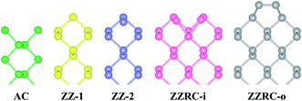 |
| | Fig. 1 Schematic view of the As NRs with different edge configurations. | |
Table 1 The calculated edge energies (eV) in the As n-NRs (n = 4, 8, 12, 16, and 20)
| |
n = 4 |
n = 8 |
n = 12 |
n = 16 |
n = 20 |
Average |
| AC |
0.30 |
0.30 |
0.30 |
0.30 |
0.30 |
0.30 |
| ZZ-1 |
0.19 |
0.19 |
0.19 |
0.18 |
0.18 |
0.19 |
| ZZ-2 |
0.31 |
0.31 |
0.31 |
0.31 |
0.31 |
0.31 |
| ZZRC-i |
0.22 |
0.22 |
0.22 |
0.21 |
0.21 |
0.22 |
| ZZRC-o |
0.15 |
0.15 |
0.15 |
0.15 |
0.14 |
0.15 |
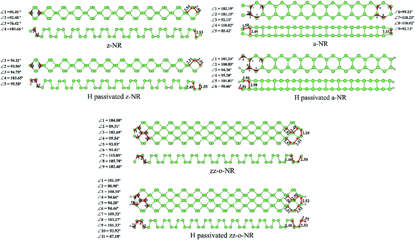 |
| | Fig. 2 Top (nearly top) and side views of the relaxed structures of the As 12-NRs with the unpassivated and H passivated edges. The green and gray balls represent As and H atoms, respectively. | |
3.2 As NRs with the AC edge
Fig. 3(a) illustrates the band structure of the unpassivated 12-a-NR, which exhibits semiconducting character with an indirect band gap. As revealed by the partial charge density [Fig. 3(a)] and the orbital-resolved band structures [Fig. S2(a)†], the valence band maximum (VBM) located near the X point (indicated by the A point) is dominated by the As px bonding states while the conduction band minimum (CBM) close to the Γ point (indicated by the B point) is dominated by the py anti-bonding states from the edge As atoms. The band edges position of the bare As a-NRs is different from the corresponding P-based a-NRs10 where the VBM is found located at the Γ point. In addition, it is observed that α and β bands split at the A point, contributed primarily by the edge and central As atoms, respectively. Due to the weaker interaction between the As atoms at the armchair edge, the unpassivated As a-NRs exhibit decreasing band gaps with increasing ribbon width n [Fig. S3†].
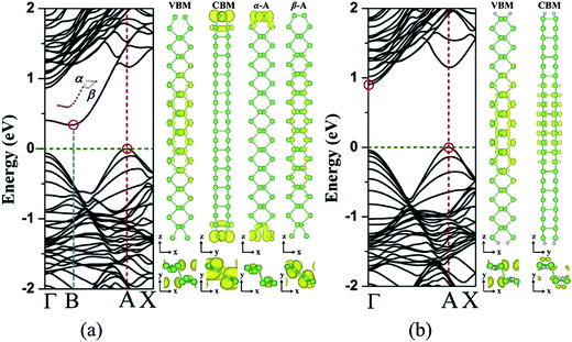 |
| | Fig. 3 Band structures of (a) the unpassivated and (b) the H passivated As 12-a-NR. Right panels show the partial charge density distribution of the VBM/CBM and the α and β bands at the A point in (a) the Fermi level is set to zero. The isosurface value is set to be 0.002 e Å−3. The VBM/CBM is indicated by red circle. | |
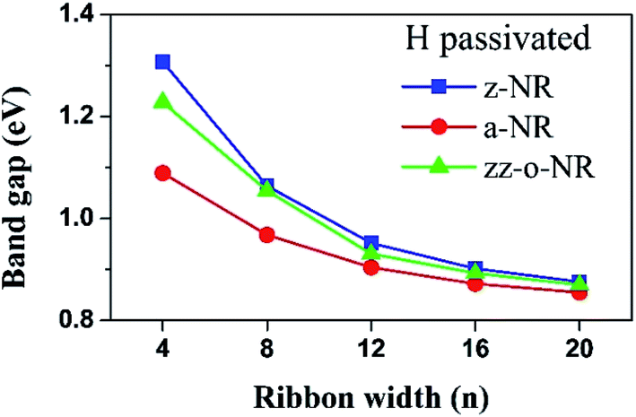
With H passivation at both edge sites, the bands in the Fermi level region are disappeared and all a-NRs exhibit semiconducting properties, as shown in Fig. S4.† Fig. 3(b) illustrates the band structure of the H passivated 12-a-NR. Different from the P a-NR with a direct band gap at the Γ point,10 the As a-NR exhibits an indirect band gap, in which the VBM and CBM are located at the A and the Γ point, respectively. Due to the quenching of the edge states, both of the VBM and CBM are contributed by the states in the central region of the nanoribbon, which are dominated by the As px and py orbitals, respectively, as indicated in Fig. 3(b) and S2(b).† The band gap of the H passivated a-NR versus ribbon width n (n = 4, 8, 12, 16, and 20) is illustrated in Fig. 4. Due to the weaker quantum confinement, the band gap decreases with increasing ribbon width and gradually approaches to that of the As monolayer (0.83 eV).17
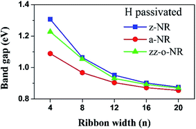 |
| | Fig. 4 Variation of the band gap of the H passivated As NRs versus ribbon width n. | |
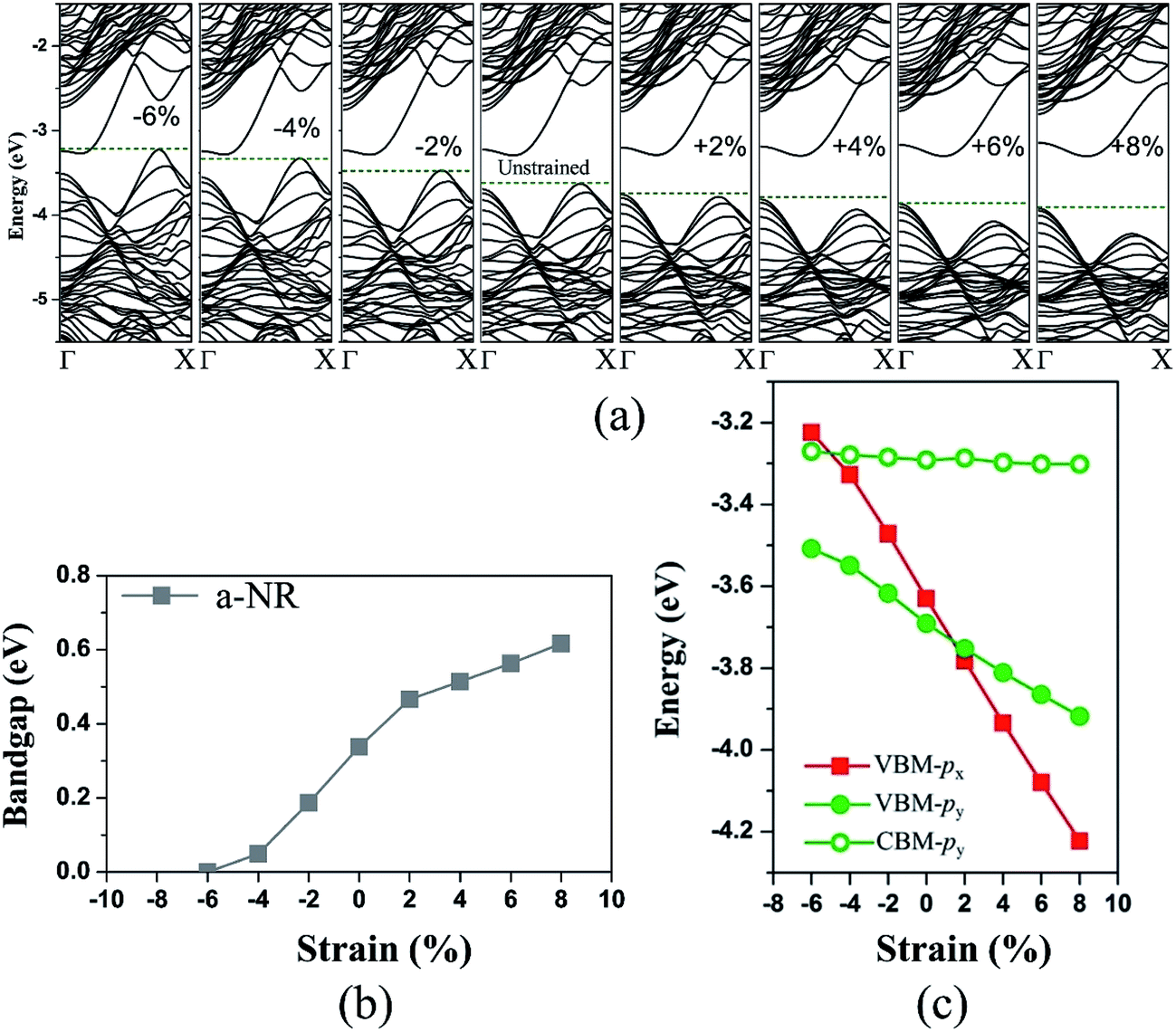
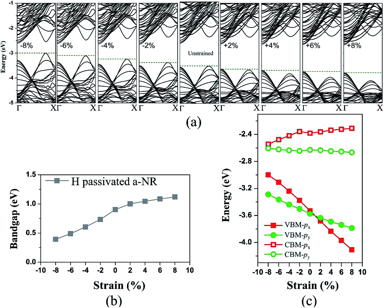
Effects of strain on the electronic properties of As a-NRs with and without H passivation at the edge are investigated. Our calculation reveals that applying strain has significant effects on both of the band gap and orbital contribution at the band edges. As revealed in Fig. 5(a) and 6(a), the band gap of the 12-a-NR increases with respect to the increasing tensile strain, accompanying by a VBM transfer from the A to Γ point. At the equilibrium lattice constant, as shown in Fig. 3(a) and (b), the As py orbitals dominated bonding states at the Γ point near the Fermi level have a comparable energy with the px states dominated VBM. When tensile strain is applied along the armchair direction, the As px bonding states are the most affected. In addition, the armchair-oriented strain also influences the As py bonding states due to the small structural relaxation perpendicularly to the armchair direction. Consequently, based on the movement of different orbitals near the Fermi level, the bonding states at the A point are most sensitive to the strain, following by the bonding and anti-bonding states at the Γ point. The tensile strain helps stabilize the bonding states characterized by those states moving to the lower energy, resulting in an increasing band gap, as shown in Fig. 5(b) and 6(b). Furthermore, since the px orbital dominated bonding states at the A point are more sensitive to armchair-oriented strain [Fig. 5(c) and 6(c)], they shift to lower energy compared with the py orbital dominated Γ states, leading to a VBM shift from the A to Γ point, as shown in Fig. S6.† Thus, the H passivated 12-a-NR undergoes a transition from an indirect-to-direct gap semiconductor, as revealed in Fig. 6(a) and S6.† On the other hand, the bonding states move to higher energy with decreasing lattice constant along the armchair direction, leading to a decreasing band gap. As shown in Fig. 5, the unpassivated 12-a-NR undergoes a semiconductor-to-metal transition under the compressive strain of 6%.
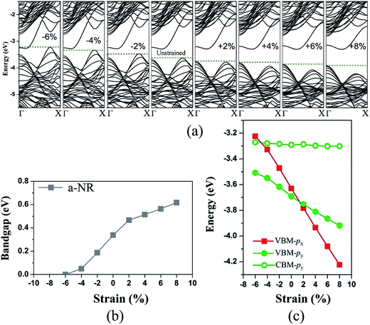 |
| | Fig. 5 Strain-dependent (a) band structures, (b) band gaps and (c) energies of the VBM/CBM states of the unpassivated As 12-a-NR. | |
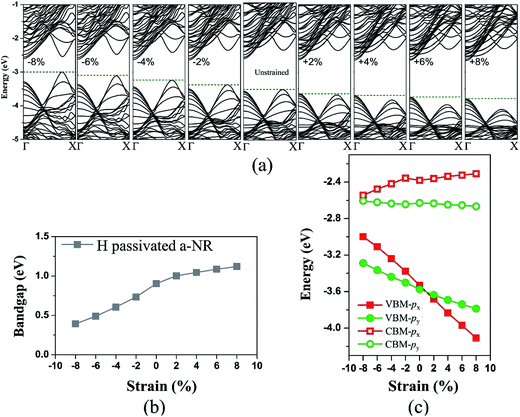 |
| | Fig. 6 Strain-dependent (a) band structures, (b) band gaps and (c) energies of the VBM/CBM states of the H passivated As 12-a-NR. | |
3.3 As NRs with the ZZ-1 edge
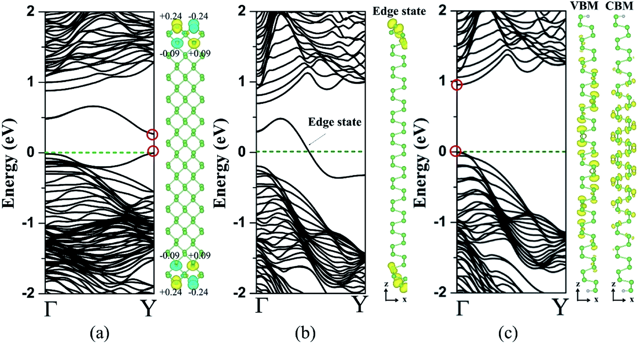
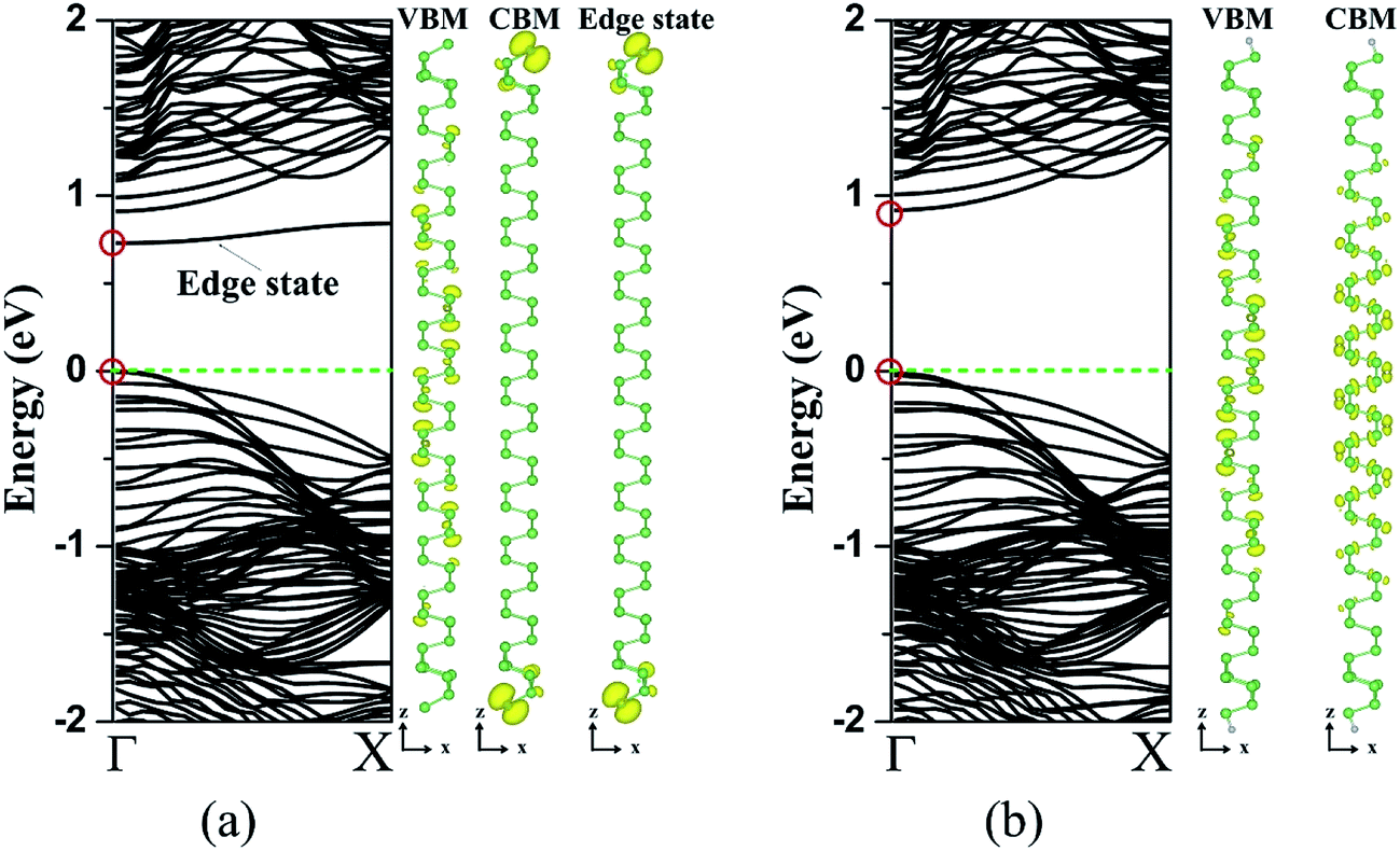
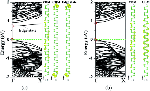
Previous study revealed that the localized electronic states at each zigzag edge in graphene nanoribbons resulted in spin polarization and half-metallicity.34,44 This motivated us to consider the stability of different magnetic coupling between the edge As atoms in the z-NRs. As described in Fig. S7,† four initial magnetic configurations are considered including ferromagnetic (FM), intra-edge FM and inter-edge AFM (AFM-1), intra-edge AFM and inter-edge FM (AFM-2), intra-edge AFM and inter-edge AFM order (AFM-3). To calculate the FM and AFM configurations in the zigzag edge, the corresponding supercells are increased to 1 × 2 × 1. Table 2 shows the relative energy difference between these magnetic states and the nonmagnetic (NM) states in the As n-z-NR (n = 8, 12, 16, and 20). The FM and AFM-1 configurations are shown to be energetically less stable than the nonmagnetic states, indicating that the FM coupling between the edge states on the same side is not favorable. Meanwhile, the AFM-2 and AFM-3 configurations where edge states are AFM aligned on the same side have much lower energies. However, the small energy difference of only several meV relative to the NM state indicates their weak magnetic coupling between the As atoms at the edges and small thermal oscillations can quench the magnetism. The AFM-2 and AFM-3 configurations are almost degenerate in energy and have similar band structures. As illustrated in Fig. 7(a), the band structure of the AFM-2 ordered 12-z-NR exhibits a semiconducting character with a direct band gap of 0.26 eV at the Y point. The Bader charge analysis indicates that the magnetic moments are mainly distributed on the As atoms at the edge sites (0.24 μB per atom) and the neighboring saturated As atoms (0.09 μB per atom). In the nonmagnetic states, similar to that of the P based z-NRs, the band structure of 12-z-NR shown in Fig. 7(b) exhibits the metallic character with two nearly degenerated edge bands crossing at the Fermi level. The corresponding orbital-resolved band structure [Fig. S2(c)†] indicates that these bands are contributed by the As pz states hybridized with the px states.
Table 2 The relative energies (eV) of the unpassivated As n-z-NRs (n = 8, 12, 16, and 20) with different magnetic configurations
| |
NM |
FM |
AFM-1 |
AFM-2 |
AFM-3 |
| 8 |
0.005 |
0.405 |
0.380 |
0.000 |
0.005 |
| 12 |
0.008 |
0.399 |
0.380 |
0.000 |
0.001 |
| 16 |
0.013 |
0.396 |
0.382 |
0.000 |
0.006 |
| 20 |
0.006 |
0.391 |
0.391 |
0.000 |
0.002 |
 |
| | Fig. 7 Band structures of (a) the unpassivated As 12-z-NR with the AFM-2 configuration, (b) the unpassivated As 12-z-NR in the nonmagnetic states, and (c) the H passivated As 12-z-NRs. The panel below shows the corresponding spin density distribution in (a), the partial charge density distribution of the edge state bands in (b) and the VBM/CBM in (c). The Fermi level is set to zero. For the spin charge density, the yellow/blue isosurface shows the positive/negative spin density with a value of 0.002 e A−3. For the partial charge density, the isosurface value is set to be 0.002 e Å−3. The VBM/CBM is indicated by red circle. The indicated magnetic moment is in the unit of μB. | |
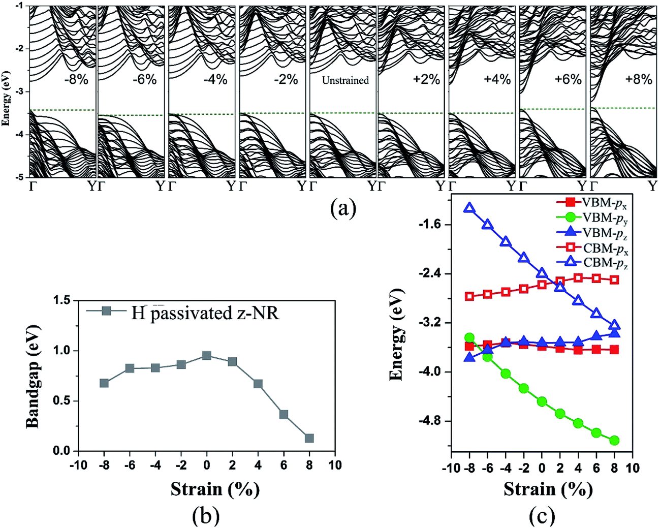
With H passivation of the edge sites, all n-z-NRs (n = 4, 8, 12, 16, and 20) exhibit nonmagnetic and semiconducting properties with a direct band gap at the Γ point, as shown in Fig. S8.† Further examination of the band structure of the 12-z-NR shows that both of the VBM and CBM are contributed by the states from the central region of the nanoribbon, dominated by the As pz and px orbitals, respectively, as shown in Fig. 7(c) and S2(d).† The ribbon width-dependent band gaps also show a similar trend with that of the H passivated a-NRs due to the quantum confinement effect, as indicated in Fig. 4.
Effects of strain on the magnetic coupling of the edge states are investigated by applying −6% to +6% zigzag-oriented strains on the 12-z-NR. The relative stability between the AFM-2 and NM states is compared by calculating the total energy differences, as outlined in Table 3. The tensile strain helps stabilize the AFM-2 state with enhanced energy differences and the magnetic moments distributed on the edge sites, as indicated in Tables 3 and 4. The strain-dependent band structures shown in Fig. 8 indicate that, under the increasing tensile strain, the 12-z-NR undergoes a direct-to-indirect-to-direct band gap transition with band edges changed from the Y to Γ point. Furthermore, the band gap increases to 0.35 eV under the strain of +3% and then decreases with increasing tensile strain. Whereas compressive strains from 0% to 4% stabilize the NM state in the 12-z-NR as indicated in Table 3. For larger compressive strain of 6%, the AFM-2 configuration becomes more stable due to the semiconducting-to-metal transition.
Table 3 The strain-dependent relative energies (eV) of the unpassivated As 12-z-NR between the NM and AFM-2 configuration
| |
+6 |
+5 |
+4 |
+3 |
+2 |
+1 |
0 |
−2 |
−4 |
−6 |
| NM |
0.141 |
0.157 |
0.080 |
0.063 |
0.040 |
0.015 |
0.008 |
0.000 |
0.000 |
0.051 |
| AFM-2 |
0.000 |
0.000 |
0.000 |
0.000 |
0.000 |
0.000 |
0.000 |
0.006 |
0.053 |
0.000 |
Table 4 Magnetic moments distribution and the band gap evolution in AFM-2 ordered unpassivated As 12-z-NR under the tensile strain. The magnetic moment and the band gap are in the unit of μB and eV, respectively
| |
+6 |
+5 |
+4 |
+3 |
+2 |
+1 |
0 |
| Mag. (edge site) |
0.53 |
0.49 |
0.45 |
0.41 |
0.37 |
0.30 |
0.24 |
| Mag. (neighboring site) |
0.12 |
0.12 |
0.12 |
0.12 |
0.12 |
0.10 |
0.09 |
| Band gap |
0.18 |
0.28 |
0.33 |
0.35 |
0.33 |
0.31 |
0.26 |
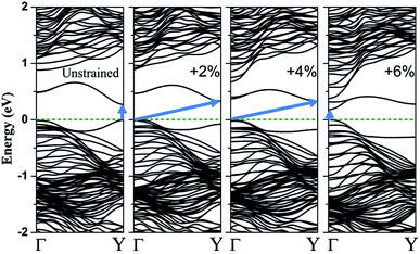 |
| | Fig. 8 Strain-dependent band structures of the unpassivated As 12-z-NR with the AFM-2 configuration. The Fermi level is set to zero. The direct/indirect band gap is indicated by the blue arrow. | |
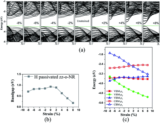
Under the influence of external strain, the electronic properties of the H passivated z-NR undergo significant changes. Fig. 9(a) illustrates the band structures of the 12-z-NR under the strain from −8% to +8%. As indicated in Fig. 9(b), the fundamental band gap of the 12-z-NR decreases under either tensile or compressive strains, which is different from the behavior in the corresponding P-based NRs.10 The orbital-resolved band structures [Fig. S9†] demonstrate that the band gap evolution is governed by the different responses of the px, py, and pz dominated bonding and anti-bonding states to the external strains. By analyzing the relaxed structures of the strained 12-z-NRs, it is found that there is significant relaxation along the ribbon width direction when the lattice is strained along the zigzag direction. As a result, the As py and pz orbitals dominated states are significantly affected under the zigzag-oriented strain. In addition, as shown in Fig. 9(c) and S9,† the tensile strain helps decrease the energy splitting between the pz anti-bonding and bonding states. This results in a decreasing band gap trend due to the downward shift of the pz orbital dominated CBM. Meanwhile, under compressive strains, the pz anti-bonding states move to higher energy, leaving the CBM characterized by the px anti-bonding states which are less affected. As discussed above, applying strain along the zigzag directions is expected to have significant effects on the py orbital dominated states. However, since the py bonding states are situated deeply inside the valence band, they only affect the VBM when the compressive strain reaches to 8%, as shown in Fig. 9(c) and S9.† Therefore, applying compressive strain only moderately reduces the band gap of the 12-z-NR and the nanoribbon preserves its semiconducting property.
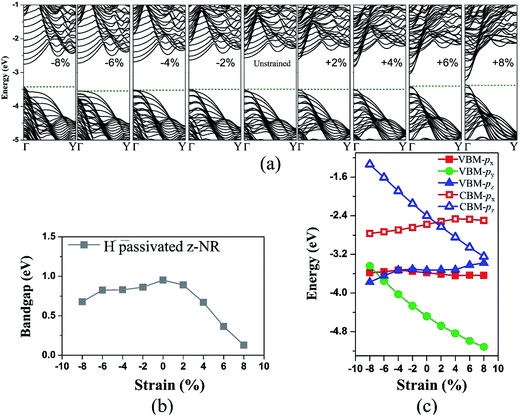 |
| | Fig. 9 Strain-dependent (a) band structures, (b) band gaps and (c) energies of the VBM/CBM states of the H passivated As 12-z-NR. | |
3.4 As NRs with the ZZRC-o edge
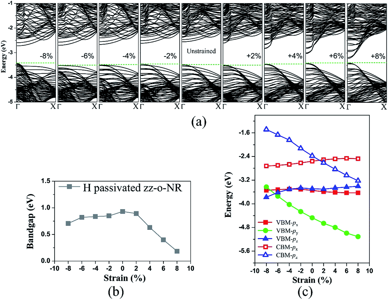
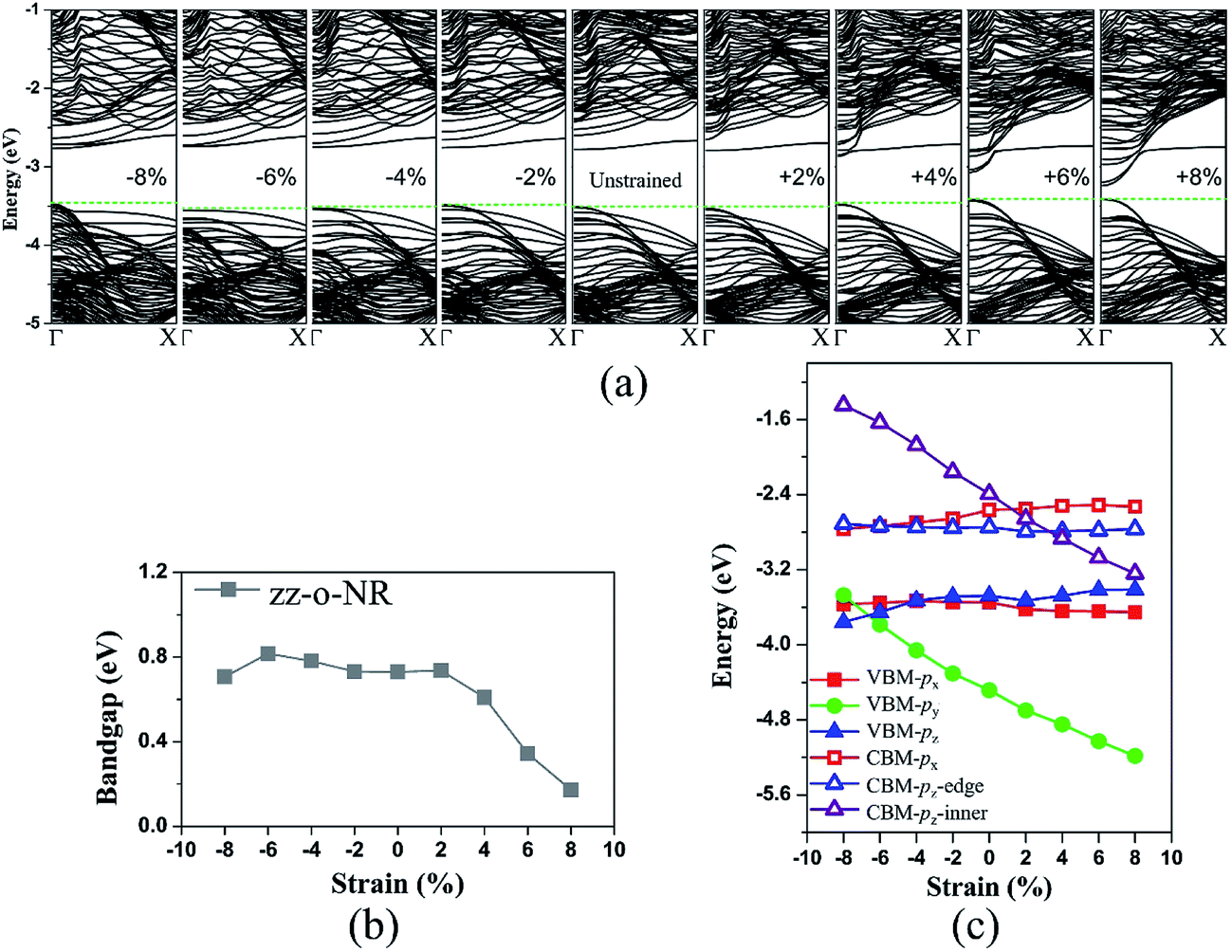
Our calculations show that both of the bare and H passivated As n-NRs (n = 4, 8, 12, 16, and 20) with the ZZRC-o edge exhibit semiconducting character with direct band gaps at the Γ point, as shown in Fig. S10(a) and (b).† Furthermore, due to the weak interaction between the As atoms at the edge, the As zz-o-NRs exhibit decreasing band gaps with increasing ribbon width n, as indicated in Fig. 4 and S10(c).†
For the 12-zz-o-NRs, the partial charge density [Fig. 10] and the corresponding orbital-resolved band structures [Fig. S2(e) and (f)†] reveal that the VBMs are contributed by the pz bonding states from the central region of the As-NRs, while the CBM originations are distinct between the bare and H passivated NRs. Specifically, for the bare zz-o-NRs, the CBM is dominated by the anti-bonding edge states with the As pz orbital character, while H passivation quenches the edge states in the Fermi level region, leading to the CBM mainly contributed by the px anti-bonding states from the central As atoms. Furthermore, in comparison with the z-NRs, the bands for the zz-o-NRs are less dispersive along the Γ–Y direction.
 |
| | Fig. 10 Band structures of (a) the unpassivated and (b) the H passivated As 12-zz-o-NR. Right panels show the partial charge density distribution of the VBM/CBM and the edge state bands in (a) the Fermi level is set to zero. The isosurface value is 0.002 e Å−3. The VBM/CBM is indicated by red circle. | |
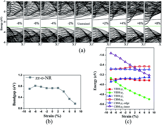
Our calculation reveals that the H passivated zz-o-NRs exhibit similar strain response with the corresponding z-NRs, due to their similar orbital contribution at the band edges, as indicated in Fig. 11 and S11.† As for the bare zz-o-NRs, there is an additional competition among the pz and/or px anti-bonding states from the edge and central As atoms. According to Fig. 12(c) and S12,† the pz anti-bonding states originated from the central As atoms move to lower energy under the effect of tensile strain, while the corresponding edge states are less affected. This results in a pz orbital characterized CBM changing from the edge site to the central region of the nanoribbon when the tensile strain increases to 4%. Meanwhile, for the zz-o NRs under the compressive strain, the energy difference between the px anti-bonding central states and the pz anti-bonding edge states at the Γ point decreases. When the compressive strain is increased to 8%, the CBM is contributed by more central As antibonding states with the px orbital character. In comparison with the compressive strain, the tensile strain has more significant effects on the band gap of the bare zz-o-NRs due to the effect of strain on the pz central anti-bonding states, as indicated in Fig. 12 and S12.†
 |
| | Fig. 11 Strain-dependent (a) band structures, (b) band gaps and (c) energies of the VBM/CBM states of the H passivated As 12-zz-o-NR. | |
 |
| | Fig. 12 Strain-dependent (a) band structures, (b) band gaps and (c) energies of the VBM/CBM states of the unpassivated As 12-zz-o-NR. | |
4. Conclusion
In conclusion, we have presented a comprehensive theoretical study of the electronic and magnetic properties of the As NRs under the effect of external lattice strain. By calculating the edge energies of different edge configurations, the reconstructed zigzag edge (ZZRC-o) is found to be the most stable. In addition, our calculations reveal that both of the unpassivated and H passivated a-NRs are indirect bandgap semiconductors, with the VBMs and CBMs dominated by the px and py states, respectively. The compressive/tensile strain leads to decreasing/increasing band gap primarily due to the shifting of the VBM at the A/Γ point. On the other hand, the zz-o-NRs and the H passivated z-NRs exhibit semiconducting character with direct band gaps at the Γ symmetry point. The corresponding VBMs are all dominated by the pz states, while the CBMs for the bare and H passivated NRs are contributed by the pz and px orbitals, respectively. Compared with the compressive strain, the tensile strain has more significant effects on these zigzag edge NRs, resulting in greatly reduced band gap. The evolution of the band edges at the Γ point is governed by the competition among the As px, py, and pz bonding and anti-bonding states from the edge site and the central region. With respect to the spin couplings between the As atoms, the unpassivated z-NRs reveal a weak AFM interaction. In addition, applying tensile strain helps stabilize the AFM states and enhance the magnetic moments distributed on the edge sites. The tensile-strained z-NRs undergo a direct-to-indirect-to-direct band gap transition due to the shifting of the band edges. Consequently, through a combination of strain tuning and edge modification, the magnetic and conductive properties can be engineered in the As-based NRs for future nanoelectronics applications.
Conflicts of interest
There are no conflicts to declare.
Acknowledgements
This work was supported by the National Natural Science Foundation of China (Grant No. 11504044). A. P. and S. L. would like to thank the financial support from Australian Research Council Discovery Program of DP150103006 and DP140104373. A. P. and F. K. acknowledge the financial support of ANSTO. The theoretical calculations were performed using the supercomputer resources at the National Supercomputer Center in Tianjin, Changsha, and the National Computing Infrastructure in Australia.
References
- G. Qin, Q. B. Yan, Z. Qin, S. Y. Yue, M. Hu and G. Su, Phys. Chem. Chem. Phys., 2015, 17, 4854–4858 RSC.
- L. Kou, C. Chen and S. C. Smith, J. Phys. Chem. Lett., 2015, 6, 2794–2805 CrossRef CAS PubMed.
- A. Jain and A. J. H. McGaughey, Sci. Rep., 2015, 5, 8501 CrossRef CAS PubMed.
- Y. Du, H. Liu, B. Xu, L. Sheng, J. Yin, C. G. Duan and X. Wan, Sci. Rep., 2015, 5, 8921 CrossRef CAS PubMed.
- S. Balendhran, S. Walia, H. Nili, S. Sriram and M. Bhaskaran, Small, 2015, 11, 640–652 CrossRef CAS PubMed.
- E. S. Reich, Nature, 2014, 506, 19 CrossRef PubMed.
- X. Peng, Q. Wei and A. Copple, Phys. Rev. B: Condens. Matter Mater. Phys., 2014, 90, 085402 CrossRef.
- Z. Y. Ong, Y. Cai, G. Zhang and Y. W. Zhang, J. Phys. Chem. C, 2014, 118, 25272–25277 CAS.
- H. Liu, A. T. Neal, Z. Zhu, Z. Luo, X. Xu, D. Tomanek and P. D. Ye, ACS Nano, 2014, 8, 4033–4041 CrossRef CAS PubMed.
- H. Guo, N. Lu, J. Dai, X. Wu and X. C. Zeng, J. Phys. Chem. C, 2014, 118, 14051–14059 CAS.
- S. Das, W. Zhang, M. Demarteau, A. Hoffmann, M. Dubey and A. Roelofs, Nano Lett., 2014, 14, 5733–5739 CrossRef CAS PubMed.
- S. Das, M. Demarteau and A. Roelofs, ACS Nano, 2014, 8, 11730–11738 CrossRef CAS PubMed.
- M. Pumera and Z. Sofer, Adv. Mater., 2017, 29, 1605299 CrossRef PubMed.
- Z. Zhu, J. Guan and D. Tomanek, Phys. Rev. B: Condens. Matter Mater. Phys., 2015, 91, 161404 CrossRef.
- S. Zhang, Y. Hu, Z. Hu, B. Cai and H. Zeng, Appl. Phys. Lett., 2015, 107, 022102 CrossRef.
- K. Luo, S. Chen and C. Duan, Sci. China: Phys., Mech. Astron., 2015, 58, 087301 CrossRef.
- C. Kamal and M. Ezawa, Phys. Rev. B: Condens. Matter Mater. Phys., 2015, 91, 085423 CrossRef.
- R. Zhao, J. Gao, Z. Liu and F. Ding, Nanoscale, 2015, 7, 9723–9730 RSC.
- L. Liang, J. Wang, W. Lin, B. G. Sumpter, V. Meunier and M. Pan, Nano Lett., 2014, 14, 6400–6406 CrossRef CAS PubMed.
- Y. Lee, J. Y. Yoon, D. Scullion, J. Jang, E. J. G. Santos, H. Y. Jeong and K. Kim, J. Phys. D: Appl. Phys., 2017, 50, 084003 CrossRef.
- P. Koskinen, S. Malola and H. Hakkinen, Phys. Rev. Lett., 2008, 101, 115502 CrossRef PubMed.
- J. Gao, X. Liu, G. Zhang and Y.-W. Zhang, Nanoscale, 2016, 8, 17940–17946 RSC.
- P. M. Das, G. Danda, A. Cupo, W. M. Parkin, L. Liang, N. Kharche, X. Ling, S. Huang, M. S. Dresselhaus, V. Meunier and M. Drndic, ACS Nano, 2016, 10, 5687–5695 CrossRef PubMed.
- C. Tao, L. Jiao, O. V. Yazyev, Y.-C. Chen, J. Feng, X. Zhang, R. B. Capaz, J. M. Tour, A. Zettl, S. G. Louie, H. Dai and M. F. Crommie, Nat. Phys., 2011, 7, 616–620 CrossRef CAS.
- K. A. Ritter and J. W. Lyding, Nat. Mater., 2009, 8, 235–242 CrossRef CAS PubMed.
- X. Jia, M. Hofmann, V. Meunier, B. G. Sumpter, J. Campos-Delgado, J. M. Romo-Herrera, H. Son, Y.-P. Hsieh, A. Reina, J. Kong, M. Terrones and M. S. Dresselhaus, Science, 2009, 323, 1701–1705 CrossRef CAS PubMed.
- C. H. Park and S. G. Louie, Nano Lett., 2008, 8, 2200–2203 CrossRef CAS PubMed.
- Y. Li, Z. Zhou, S. Zhang and Z. Chen, J. Am. Chem. Soc., 2008, 130, 16739–16744 CrossRef CAS PubMed.
- E. J. Kan, Z. Li, J. Yang and J. G. Hou, J. Am. Chem. Soc., 2008, 130, 4224–4225 CrossRef CAS PubMed.
- F. Cervantes-Sodi, G. Csanyi, S. Piscanec and A. C. Ferrari, Phys. Rev. B: Condens. Matter Mater. Phys., 2008, 77, 165427 CrossRef.
- O. Hod, V. Barone, J. E. Peralta and G. E. Scuseria, Nano Lett., 2007, 7, 2295–2299 CrossRef CAS PubMed.
- M. Y. Han, B. Oezyilmaz, Y. Zhang and P. Kim, Phys. Rev. Lett., 2007, 98, 206805 CrossRef PubMed.
- Y. W. Son, M. L. Cohen and S. G. Louie, Nature, 2006, 444, 347–349 CrossRef CAS PubMed.
- M. Fujita, K. Wakabayashi, K. Nakada and K. Kusakabe, J. Phys. Soc. Jpn., 1996, 65, 1920–1923 CrossRef CAS.
- L. Ao, A. Pham, H. Y. Xiao, X. T. Zu and S. Li, Phys. Chem. Chem. Phys., 2016, 18, 7163–7168 RSC.
- S. Zhao, W. Kang and J. Xue, Appl. Phys. Lett., 2014, 104, 133106 CrossRef.
- H. Guo, N. Lu, L. Wang, X. Wu and X. C. Zeng, J. Phys. Chem. C, 2014, 118, 7242–7249 CAS.
- H. Pan and Y. W. Zhang, J. Phys. Chem. C, 2012, 116, 11752–11757 CAS.
- P. Lu, X. Wu, W. Guo and X. C. Zeng, Phys. Chem. Chem. Phys., 2012, 14, 13035–13040 RSC.
- G. Kresse and J. Furthmuller, Phys. Rev. B: Condens. Matter Mater. Phys., 1996, 54, 11169 CrossRef CAS.
- P. E. Blöchl, Phys. Rev. B: Condens. Matter Mater. Phys., 1994, 50, 17953 CrossRef.
- J. P. Perdew, K. Burke and M. Ernzerhof, Phys. Rev. Lett., 1996, 77, 3865–3868 CrossRef CAS PubMed.
- H. J. Monkhorst and J. D. Pack, Phys. Rev. B: Solid State, 1976, 13, 5188 CrossRef.
- Y. W. Son, M. L. Cohen and S. G. Louie, Phys. Rev. Lett., 2006, 97, 216803 CrossRef PubMed.
Footnote |
| † Electronic supplementary information (ESI) available. See DOI: 10.1039/c7ra05137a |
|
| This journal is © The Royal Society of Chemistry 2017 |
Click here to see how this site uses Cookies. View our privacy policy here. 
 Open Access Article
 This Open Access Article is licensed under a Creative Commons Attribution-Non Commercial 3.0 Unported Licence
 *bc,
Xia Xiang*a,
Frank Klosecd,
Sean Lib and
Xiaotao Zua
*bc,
Xia Xiang*a,
Frank Klosecd,
Sean Lib and
Xiaotao Zua