
 Open Access Article
 This Open Access Article is licensed under a Creative Commons Attribution-Non Commercial 3.0 Unported Licence
Large-scale and facile synthesis of silver nanoparticles via a microwave method for a conductive pen†
Yaguo Caia,
Xianqing Piao *ab,
Wei Gaob,
Zhejuan Zhangab,
Er Niea and
Zhuo Sunab
*ab,
Wei Gaob,
Zhejuan Zhangab,
Er Niea and
Zhuo Sunab
aEngineering Research Center for Nanophotonics and Advanced Instrument, Ministry of Education, East China Normal University, Shanghai 200062, People's Republic of China. E-mail: piaoxianqing@163.com
bShanghai Industrial Technology Institute, No. 200 Jinsu Road, Pudong New District, Shanghai, 201206, People's Republic of China
First published on 6th July 2017
Abstract
In this study, we report a large-scale and facile synthetic method for silver nanoparticles via a microwave method, which is quite time-saving and efficient. The obtained silver nanoparticles maintained a uniform size, and the average size was less than 20 nm although the concentration of the silver source was very high. The obtained silver nanoparticles could be homogeneously dispersed in deionized water, which was beneficial for the fabrication of the conductive ink. For large-scale industrialization, the synthetic process window was widened to a great extent via a series of experiments. We injected the ink into a blank mark pen to fabricate a conductive pen, via which the tracks drawn on the photo paper could immediately become conductive at room temperature with an electrical conductivity of 2.4 μΩ cm (about 1.5 times that of the bulk Ag). The mechanical properties of the tracks were examined for a twistable application. After bending at a radius of 4 mm and 2 mm for 5000 circles, only a slight increase in their resistance of 1.20 and 1.78 relative to their initial resistance, respectively, was observed. The as-prepared conductive ink and fabricated pen have potential applications in flexible electronics.
1. Introduction
Recently, more and more people have been attracted to printed electronics that show great potential in various applications such as radio-frequency identification devices (RFID),1 photovoltaic cells,2 light-emitting diodes (LEDs),3 SERS,4,5 organic thin film transistors (OTFT),6 smart clothing,7 and sensors.8 Rapid and cost-effective methods for the fabrication of electronics on flexible substrates, such as polymers,9 cloth textiles,7,10 and paper,11 are important for the realization of commercially available flexible electronics. Polyethylene terephthalate (PET) is a kind of common plastic that is widely used as the flexible substrate. However, the highest temperature that it can resist is about 150 °C. In addition, the mismatch of the thermal and mechanical properties of the substrate and conductive line leads to poor adhesion between the functional circuit and the substrate. Therefore, low annealing temperature is necessary for further applications. To improve the efficiency, a roll to roll manufacturing configuration would be a great advantage. However, it is very difficult to accommodate this configuration in conventional photolithographic or vacuum-based microfabrication systems. Thus, a simple and quick method for the fabrication of metal patterns on flexible polymer substrates without photo-masking, vacuum deposition, and harsh chemical processes is essential. To date, several types of fabrication technologies, including inkjet printing,12 nanoimprinting,13 deposition and mild temperature processes using solution based on nanomaterials,14 laser-induced transfer of materials,15 laser ablation of pre-deposited materials,16 and laser sintering of nanomaterials, have been developed for flexible electronics.17 To obtain high conductivity, the organic materials should be removed from the pattern as far as possible. Moreover, to realize low sintering temperature, the size of the nanoparticles should be small enough such that it does not sacrifice the yield. This is because the smaller the nanoparticles, the lower the sintering temperature.To date, various synthesis methods for nanoparticles18–22 have been reported. Xia et al.23 have researched the morphology and growth mechanism of silver nanoparticles in detail. Usually, some controlling agents are required to achieve a uniform morphology. As is known from most of the reported studies,11,24 to obtain small nanoparticles, the concentration of the silver source should be usually at the millimole level. Moreover, strong reducing agents such as hydrazine hydrate, sodium borohydride, and 1,4-benzenediol (hydroquinone) were usually used in the process, which burdened the environment. Therefore, improvements are still needed from the viewpoint of rapid synthesis of silver nanoparticles and high quality and widening of the synthetic process window for the efficient synthesis of desirable silver nanoparticles.
In addition to decreasing the size of the particles, a better sintering method is also important. To date, several methods have been put forward including thermal sintering,25 plasma sintering,24,26,27 photonic sintering,28,29 laser sintering,30–32 microwave sintering,33 and chemical sintering.34–36 Among these, chemical sintering is a promising method because it does not need external energy and can be realized at room temperature. To date, to realize room temperature sintering, the track is usually chemically treated using hydrochloric acid, halide, and organic materials with halogen elements.37 To the best of our knowledge, the earliest study on chemical sintering was reported by Werner Zapka et al.38 In their experiment, they found that halides were a key factor to achieve efficient curing; especially chlorine salts, which produce halogen ions with the smallest size, showed the best sintering at room temperature. It was speculated that due to the small size, chlorine ions diffuse well through the polymeric shell and attach to the silver particles to form insoluble silver salts and thus displace the polymer shell on the particle surface. Furthermore, Shlomo Magdassi et al.37 also reported that the destabilizing agent, which contains Cl− ions, caused detachment of the anchored groups of the stabilizer from the surface of the nanoparticles and thus enabled their coalescence and sintering.
In this study, we experimentally developed a facile and efficient method to synthesize silver nanoparticles. In contrast to other mini-amount output methods (that cannot produce Ag nanoparticles on the gram scale), we used a microwave-supported device to synthesize silver nanoparticles and realized large-scale production. Furthermore, the obtained silver nanoparticles were used in the conductive pen, and the track drawn on the photo paper immediately became conductive at room temperature with a quite high conductivity of 2.4 μΩ cm, which was only 1.5 times that of the bulk silver. The obtained silver nanoparticles were uniform, and the average size was less than 20 nm although the concentration of the silver salt of the precursor solution was as high as 20 wt%. The thermal properties and mechanical properties of the tracks were checked to meet the application requirements via a series of measurements. With the conductive pen, conductive circuits were directly drawn for flexible devices such as LEDs and sensors; this indicates that the as-prepared conductive material has applications in flexible electronics.
2. Experimental
2.1 Materials
All the reagents were purchased and used without additional purification. Silver nitrate (AgNO3, AR), ethanol (CH3CH2OH, AR), and monoethanolamine (MEA, AR) were purchased from Sinopharm Chemical Reagent Co. Ltd. Poly (acrylic acid) (PAA, Mw = 3000) was obtained from Aladdin Reagent Co. Ltd. Deionized water (DI water, resistance of 18.2 MΩ cm) was used in all the experiments. The substrates used in this study were bright white photo paper (200 g m−2) and high glossy photo paper (240 g m−2), which were obtained from Shanghai Elite Office Supplies Co. Ltd. in China, and the Fuji Film photo paper was obtained from Real Colour Co. Ltd. in China.2.2 Synthesis of silver nanoparticles
In the synthesis of silver nanoparticles, silver nitrate was used as a silver source, MEA was used as a reducing reagent, PAA was used as a capping agent, and DI water was used as a medium. The detailed description of the synthesis of silver nanoparticles is as follows: 6 g of MEA and 0.5 g of PAA were sequentially dissolved in 25 g DI water, and the mixture was vigorously stirred at room temperature to form solution A. Then, 5 g AgNO3 was dissolved in a certain amount of DI water (5, 10, 20, and 30 g) as a silver source for solution B. Then, solution B was added to solution A and continuously stirred for some time (2 h, 1 h, 0.5 h, and 2 min) to form a uniform mixture. After stirring, the clear solution was treated in a household microwave oven at 700 W for 1 min to obtain a solution of silver nanoparticles, which was further diluted using ethanol. Then, the PAA-coated silver nanoparticles were obtained via centrifugation and washed three times with ethanol to remove the residual impurities. Eventually, the obtained precipitates were dispersed in DI water for further use.2.3 Preparation of the conductive pen
Typically, 1 g of precipitates, obtained via centrifugation, was dispersed in 2 g of DI water, stirred for several minutes, and the solution was treated via ultrasonication for 30 min. Then, a brownish-red conductive ink was prepared. The ink was further filtered through a 0.45 μm filter and absorbed into the refill via capillary force; thus, the conductive pen was successfully fabricated.2.4 Characterization
X-ray diffraction (XRD) was conducted using a Rigaku UltimaIV X-ray diffractometer with Cu Kα radiation (λ = 0.1542 nm). The morphology of the silver nanoparticles and the tracks were investigated via a Hitachi S-4800 scanning electronic microscope (SEM), and the high-resolution images and selected area electron diffraction (SAED) pattern were obtained by a transmission electron microscope (TEM). The UV-vis spectra were obtained using a Hitachi U-3900 spectrophotometer operating in the normal mode. The Raman spectrum was obtained using the IDRaman micro 785 (Ocean Optics, Inc.). The sheet resistance and thickness of the conductive track were measured by a four-point probe system (RTS-8, Four Probes Tech Co. Ltd.). The adhesion of the silver film to photo paper substrate was carried out using an ASTM D3359 tape-test standard: one part of the film was cut into 100 small squares; 3M tape was glued to the 100 small squares; the tape was then pulled off and the number of detached squares was counted via digital microscope observation (3R Anyty). The mechanical properties of the tracks were determined by a HF-9012 constant temperature fatigue testing machine (Ligao Testing Equipment Co. Ltd.).3. Result and discussion
Fig. 1 shows the synthetic scheme for the preparation of silver nanoparticles via a microwave method and the as-prepared conductive pen. The precursor solvent was composed of silver nitrate, MEA, PAA, and DI water, acting as a silver source, reducing reagent, capping agent, and medium, respectively. In the mixture, the lone pair electrons of nitrogen in MEA effectively combined with Ag+ in the solution and thus controlled the speed of the reaction. In addition, the hydroxyl group formed an aldehyde group via heating, which reduced Ag+ to Ag0. Moreover, PAA covered the silver nanoparticles for a steric effect, which resulted in a good dispersion of the obtained silver nanoparticles. The classical mechanism was proposed by LaMer and co-workers39 in the early 50's. In the synthesis of nanoparticles, the concentration of metal atoms steadily increased with the precursor decomposition. Once the concentration of the atoms reached a point of supersaturation, the atoms began to aggregate into small clusters via self-nucleation. Once formed, these nuclei then grew in an accelerated manner, the concentration of the atoms quickly dropped below the level of minimum supersaturation, and then no additional events occurred. With a continuous supply of Ag atoms via ongoing precursor decomposition, the nuclei will grow into nanocrystals of increasingly larger size until an equilibrium state is reached between the atoms on the surface of the crystal and the atoms in the solution. Because microwave heating is very fast and the microwave field is uniform, a large number of silver nuclei are formed in a short time. Furthermore, due to the limited silver source and the existence of the capping agent-PAA, the average size of the silver nanoparticles was quite small and uniform.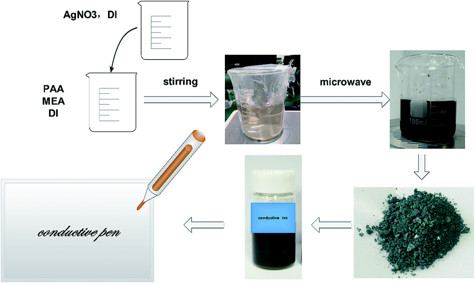 | ||
| Fig. 1 Synthetic scheme for the preparation of silver nanoparticles by a microwave method. | ||
Fig. 2a–d show the representative SEM images of the as-obtained silver nanoparticles for different concentrations of silver nitrate (5 g silver nitrate dissolved in 5, 10, 20, and 30 g of DI water, respectively.) At high concentrations (the mass ratio of AgNO3 to DI was 1![[thin space (1/6-em)]](https://www.rsc.org/images/entities/char_2009.gif) :1), as shown in Fig. 2a, there were some island-like silver particles due to the aggregation of the small particles for high surface free energy and high concentration. With the decreasing concentration of silver nitrate, the island-like silver disappeared. As shown in Fig. 2c and d, the nanoparticles were well dispersed and uniform, and the size of the nanoparticles was less than 20 nm. Fig. 2e shows the UV-vis spectra of the nanoparticles for different concentrations of silver nitrate. At high concentrations of AgNO3 (the mass ratio of AgNO3 to DI was 1:1), except for an obvious peak at 425 nm, an additional band at 635 nm appeared, indicating that the nanoparticles were not uniform, which was in accordance with the morphology shown in Fig. 2a. As the concentration decreased, there was only one unique peak at about 420 nm, and the peak became narrow, which meant that the uniformity in the size of the nanoparticles was very good. The peak located at 420 nm was the typical plasma resonance peak of silver nanoparticles. The above mentioned results indicated that the optimal concentration for synthesizing uniform silver nanoparticles was 1:4 by mass ratio.
:1), as shown in Fig. 2a, there were some island-like silver particles due to the aggregation of the small particles for high surface free energy and high concentration. With the decreasing concentration of silver nitrate, the island-like silver disappeared. As shown in Fig. 2c and d, the nanoparticles were well dispersed and uniform, and the size of the nanoparticles was less than 20 nm. Fig. 2e shows the UV-vis spectra of the nanoparticles for different concentrations of silver nitrate. At high concentrations of AgNO3 (the mass ratio of AgNO3 to DI was 1:1), except for an obvious peak at 425 nm, an additional band at 635 nm appeared, indicating that the nanoparticles were not uniform, which was in accordance with the morphology shown in Fig. 2a. As the concentration decreased, there was only one unique peak at about 420 nm, and the peak became narrow, which meant that the uniformity in the size of the nanoparticles was very good. The peak located at 420 nm was the typical plasma resonance peak of silver nanoparticles. The above mentioned results indicated that the optimal concentration for synthesizing uniform silver nanoparticles was 1:4 by mass ratio.
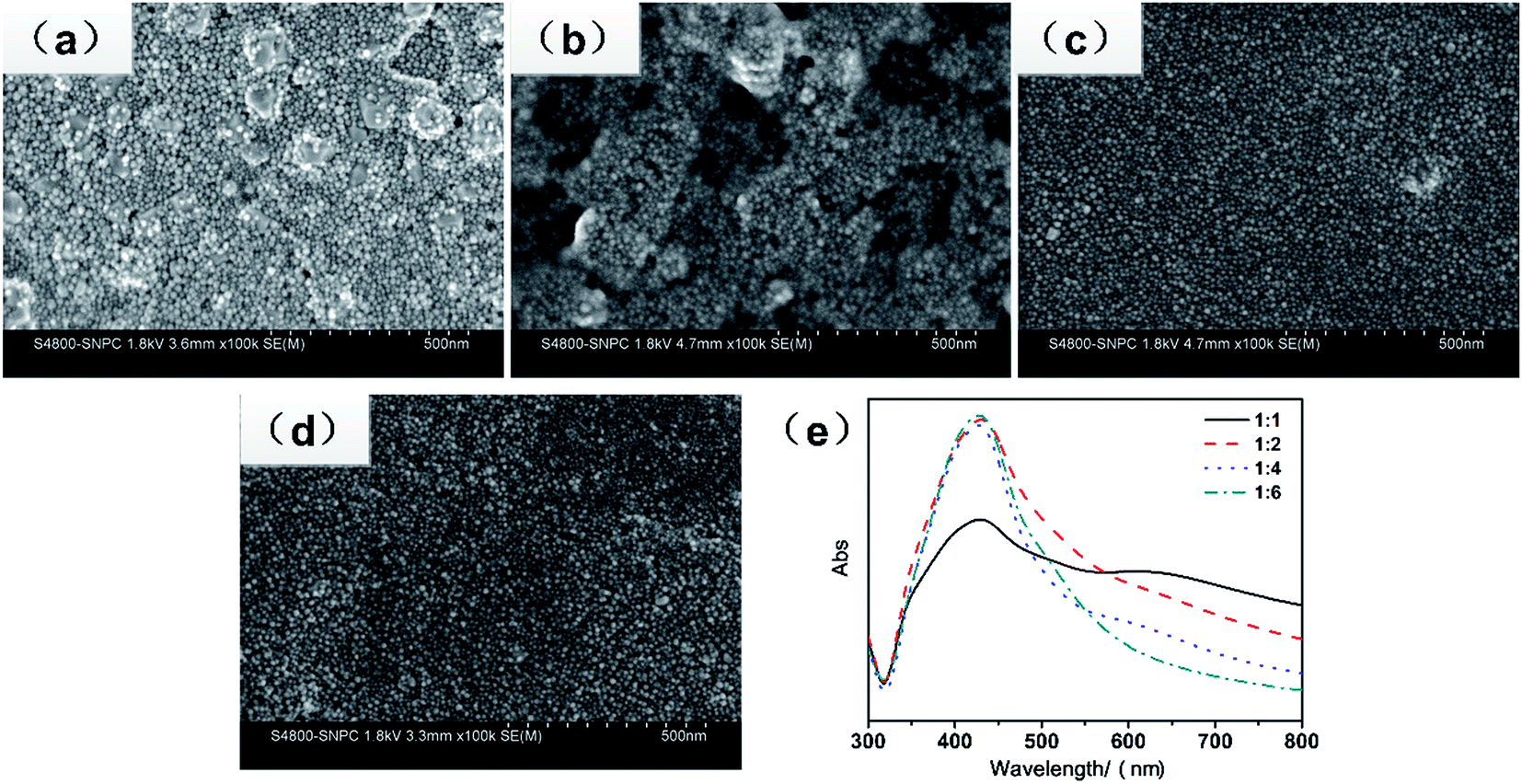 | ||
| Fig. 2 (a–d) SEM images of the silver nanoparticles synthesized at the mass ratio of silver nitrate to water is 1:1, 1:2, 1:4, and 1:6, respectively, and (e) UV-vis spectra of the silver nanoparticles at different concentrations of silver nitrate. | ||
In the experiment, at first, the stirring time of the mixture was set to 20 h. We found that during stirring of the mixture, the solvent changed from light yellow to red, which meant that some reactions occurred. It was necessary to find out if the stirring time had an effect on the final result. We set the stirring time at 2 h, 1 h, 0.5 h, and 2 min, whereas the other variables were kept constant. The SEM images in Fig. S1a–d† show that there is almost no obvious change in morphology, and all particles are nanoparticles. Fig. 3a shows the UV-vis spectra of the nanoparticles at different stirring times, and the peaks are located at about 420 nm. With the decreasing stirring time, the half-peak width became narrow, which confirmed that the synthesized nanoparticles were uniform. However, when the stirring time was too short, i.e. 2 min, the size distribution was not very good. Fig. 3b is a high-resolution image of silver nanoparticles with a stirring time of 30 min. It can be observed that the nanoparticles were uniform, and no obvious glomeration occurred. The size distribution of the nanoparticles was measured by Nano Measure software. We selected 200 nanoparticles and measured their size. The result is shown in Fig. 3c, which indicates that most of the particles are smaller than 20 nm. Thus, the stirring time played a limited role in their size and uniformity. In a large scale production, by minimizing the time of the stirring process, the preparation efficiency could be improved. Note that a microwave-supported device can be transformed into a continuous microwave reactor to increase the production.
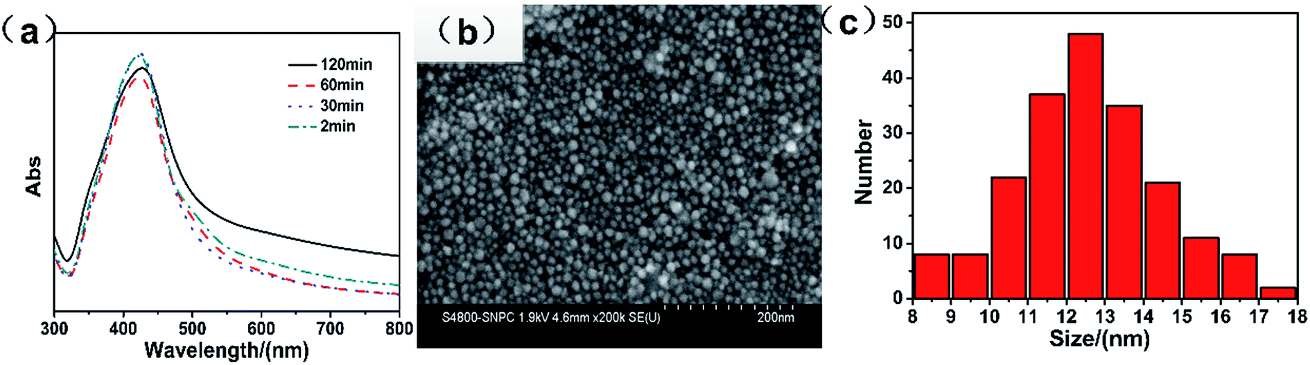 | ||
| Fig. 3 (a) UV-vis spectra of the silver nanoparticles at different stirring times, (b) the SEM pictures of silver nanoparticles stirred for 30 min, and (c) the size distribution. | ||
The other possible influencing factors, including the power and microwave time, the concentration of PAA, and the kind of surfactant, were also investigated to enhance the synthesis quality and productivity. When the microwave irradiation was added to the mixture, the main solvent water, a dipolar molecule, absorbed energy from the microwaves by oscillating back and forth, which rapidly increased the temperature, thus accelerating the reduction of silver ions.40 Because of the uniform distribution of the electromagnetic field, a homogeneous temperature field can be formed. In addition, a hydrogen free radical and hydroxyl free radical, formed by the breakage of the hydrogen bond of the water molecule due to high-speed rotation, could also accelerate the reduction process.41 The corresponding results of the performance of the microwave are shown in Fig. S2;† when the power changed from 210 W to 700 W, the silver nanoparticles of high quality could be achieved at a proper time, which was confirmed by the UV spectra (as shown in Fig. S3†), revealing a single absorption peak at about 420 nm. By tuning the power and time, it was found that the total energy (power × time) was optimized in a certain range of 700–850 W min/100 mL. When the total energy exceeded this range, aggregation or precipitation occurred, which was irreversible, and the aggregates or precipitates were difficult to redisperse. On the contrary, silver ions could not be completely reduced if the total energy was less than 700 W min, resulting in low productivity.
Based on the particular principle of microwave heating, silver nanoparticles with a small size could be synthesized in a very short time (several minutes). To prove the special effect of the microwave method, we also synthesized silver nanoparticles via ultrasonic heating and water bath heating, with the same concentration of all agents except for the heating route. The results are compared in Fig. S7.† via ultrasonic heating, uniform silver nanoparticles could also be synthesized, but a long stirring time and ultrasonic time over one day were necessary. However, the agglomeration was serious and some large particles appeared via the method of water bath heating. Therefore, the microwave method was superior to other conventional methods, especially for rapid synthesis and large scale production of Ag nanoparticles.
Fig. S4 and 5† show the impact of the amount of PAA. Without the addition of PAA, large particles with a size of about 500 nm were obtained; this indicated that PAA surfactant played a great role in the depression of nanoparticle growth. Via adjusting the amount of PAA, uniform silver nanoparticles were synthesized. Furthermore, the role of different surfactants in the morphology of the products is compared in Fig. S6.† It was observed that PAA was more suitable to synthesize high-quality silver nanoparticles than other surfactants.
A representative TEM image obtained for the silver nanoparticle deposited on a carbon-coated copper TEM grid is shown in Fig. 4a. It shows that most of the particles are spherical in shape with a size smaller than 20 nm, consistent with Fig. 3b, which has a narrow surface plasma resonance band at 420 nm. The crystalline nature of the silver nanoparticles was confirmed by the SEAD pattern (Fig. 4b), which showed the quasi-ring-like diffraction pattern, demonstrating that the polycrystalline structure was formed, and the (111), (200), (220), (311) and (222) rings were indexed to the face-centered cubic (fcc) crystal structure of Ag. The crystalline nature of a single particle was further investigated via high resolution (HRTEM) images, which showed the presence of lattice fingers with d-spacing values. As shown in Fig. 4c, two groups of lattice fringes are clearly resolved, and the lattice distances are 0.24 and 0.20 nm, indexing to the (111) and (200) crystal planes of Ag, respectively.
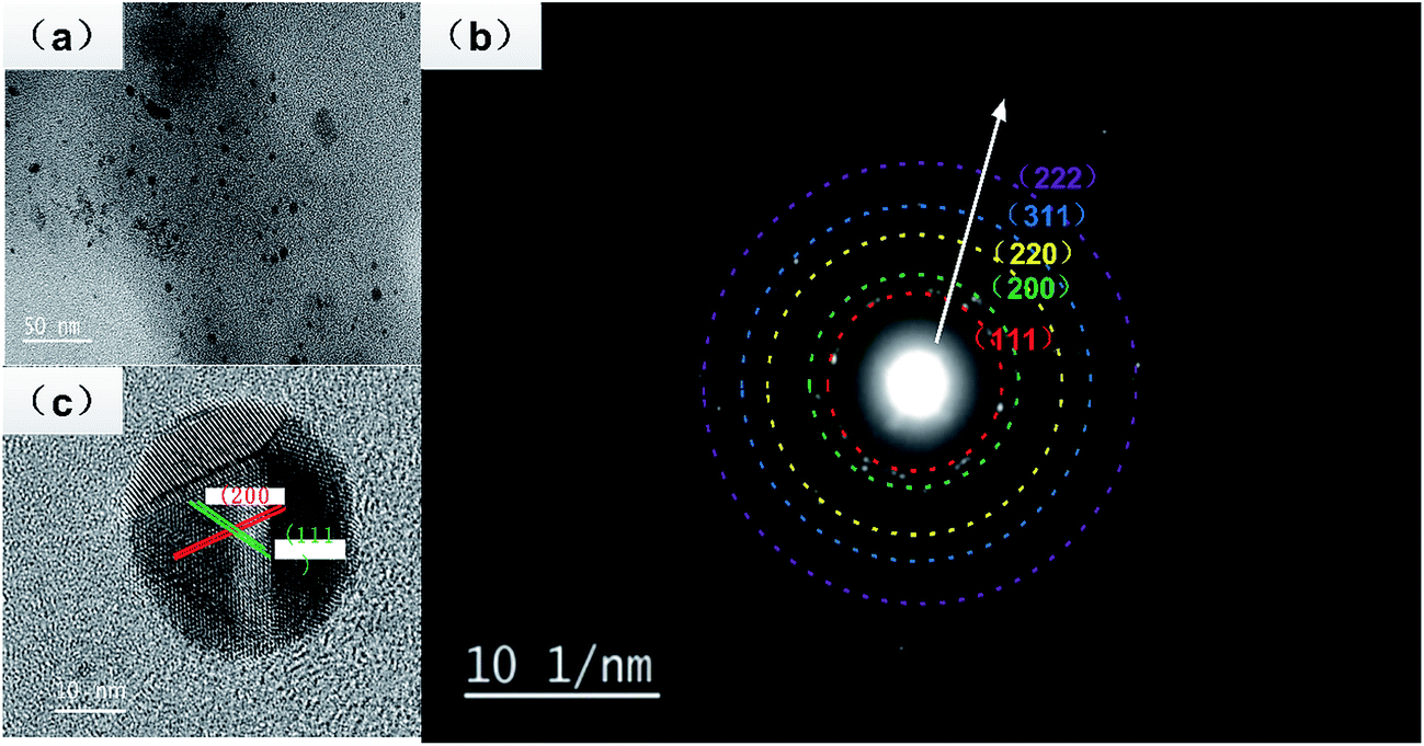 | ||
| Fig. 4 (a) TEM image of the silver nanoparticles, (b) the SAED patterns, and (c) the high-resolution TEM image. | ||
Fig. 5 shows the XRD patterns of the synthesized silver nanoparticles obtained in the 2θ range from 30° to 90°. This data is in agreement with the values for a face-centred cubic (fcc) crystal structure of silver. The peaks at 38.2°, 44.4°, 64.5°, 77.5°, and 81.6° correspond to the (111), (200), (220), (311), and (222) crystal planes. No other peaks for any impurities were detected. The crystallite size of silver nanoparticles calculated by XRD analysis (using Scherrer's equation, with (111) as the most intense plane) was 7 nm, which was a little smaller than that obtained from SEM, but close to the result of TEM. For smaller nanoparticles (≤15 nm), the crystallite size closely matched with the corresponding TEM-derived particle size.42,43 This further validated our earlier discussion that the smallest nanoparticles appeared to be primarily in their monocrystalline form. Benefiting from the fast synthetic procedure, the uniform silver nanoparticles could be easily synthesized.
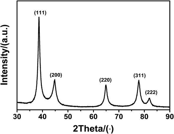 | ||
| Fig. 5 The X-ray diffraction pattern of the as-prepared silver nanoparticles. | ||
Once the pattern was drawn on the photo paper, the conductive tracks were immediately realized and became stable in resistance. In a previous study,44,45 the tracks needed to undergo further heat treatment. Herein, the specimens were heat-treated in an oven at different temperatures and times. The electrical resistance property (R/R0) as a function of the temperature and time is shown in Fig. 6a. The ratio of R/R0 is in the range from 0.9 to 1.2. Generally, heat treatment at higher temperatures is beneficial for the development of the electrical conductivity. However, the conductivity of tracks with further treatment unexpectedly decreased, even lower than of those without further treatment. From the optical microscopy observations of the test specimens, as shown in Fig. 6c–f, we found that without heating, the film was unbroken and smooth, whereas an obvious crack formed after heat treatment. The more the cracks, the lower the electrical conductivity. It was ascribed to the mismatch of the thermal property between the silver track and the photo paper. At high temperatures, the polymer on the surface of photo paper dramatically expanded; this resulted in the brokage of the Ag layer. Fig. 6b shows the SEM image of the track on the photo paper; it shows that the silver particles melted together and formed well conducting routes, which were beneficial for high conductivity. Thus, a further heat treatment was not helpful to improve the conductivity because of the spreading of the micro crack. In addition, the optimal electrical conductivity of the track was 2.4 μΩ cm, which was about 1.5 times that of the bulk silver.
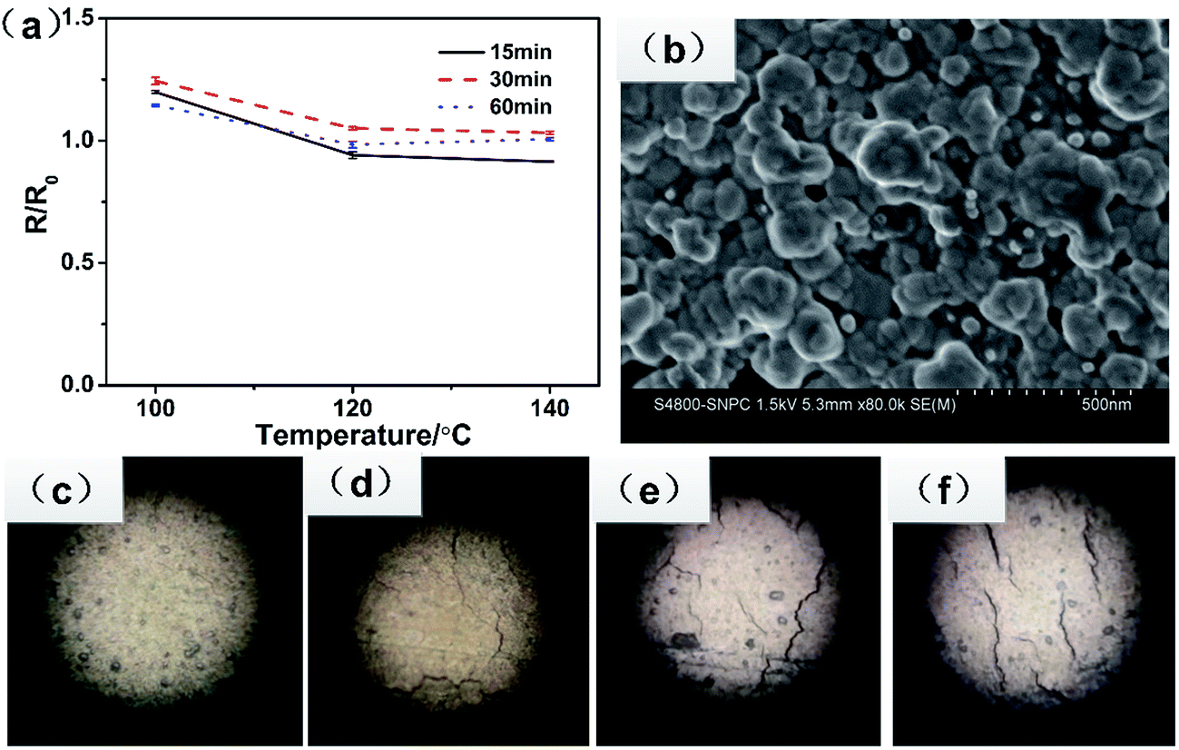 | ||
| Fig. 6 (a) The R/R0 as a function of heating temperature and heating time, (b) SEM image of the track without heating. (c–f) The optical images of the tracks at different heating temperatures-without heating, 100, 120, and 140 °C, respectively. | ||
In addition, the tracks on various photo papers were examined, and the surface details are shown in Fig. S8.† In general, the photo paper was made up with a fiber base and functional coating. To improve the gloss of the photo paper, the surface was modified with nanoparticles such as alumina and silicon dioxide. Between nanoparticles, there were many voids, which helped in the quick absorption of the ink because of the capillary force. During the preparation of the coating materials, the inorganic nanoparticles were pre-coated by a surfactant. In the case of silicon dioxide, usually a cationic fixing agent, such as polyethylene imine (PEI), poly dimethyl diallyl ammonium chloride (PDADMAC), and polyvinyl amine, is used. As abovementioned, PDADMAC could play a role in curing the silver nanoparticles via chemical sintering. Too test the proposed hypothesis, the ingredient of the silicon dioxide coating was comprehensively examined. Via adjusting the ratio of the ingredients, we successfully prepared the coating layer, as shown in Fig. S9,† that could realize sintering at room temperature. Therefore, the properties of the coating layer on the photo paper were an important factor for the formation of highly conductive tracks.
Moreover, we explored the adsorption mechanism of the capping agent by checking the Raman spectra of the silver nanoparticles acquired at the 785 nm excitation. The result is shown in Fig. 7, where the strongest SERS peaks are at 1391 cm−1, 855 cm−1, and 229 cm−1, which are attributed to the νsO–C–O, νsC–C, and νAg–OCO− bands, respectively.46 These peaks clearly indicated that the main interaction of the capping agent (PAA) with the Ag surface was through the carboxylic group, i.e. through the Ag–O interaction (the moderate 855 cm−1 peak indicated that there was also an interaction through the hydrophobic part of the polymer). Note that a possible mechanism that may be involved is the desorption of PAA from the surface of the nanoparticles due to the electrostatic interaction with PDADMAC,47 leaving particles without their capping agent and enabling their coalescence.
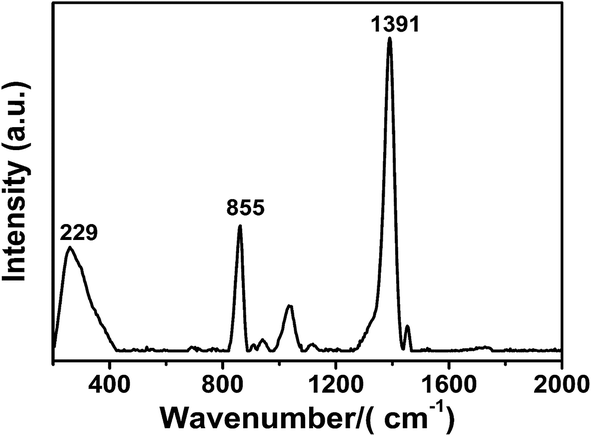 | ||
| Fig. 7 The Raman spectra of the silver nanoparticles acquired at 785 nm excitation. | ||
The mechanical flexibility of the tracks on the photo paper was determined via bending and folding tests (Fig. S10†). The electrical resistance property (R/R0) as a function of the bend radius and the number of bend cycles is shown in Fig. 8a. The silver tracks drawn on the photo paper exhibited good electrical performance over 5000 bending cycles, with only a slight increase in their electrical resistance of 1.20 and 1.78 relative to their initial resistances at the bending radii of 4 mm and 2 mm, respectively. It was clear that the conductive tracks drawn on the photo paper could maintain their electrical function even after repeated bending with a small bending radius of 2.0 mm.
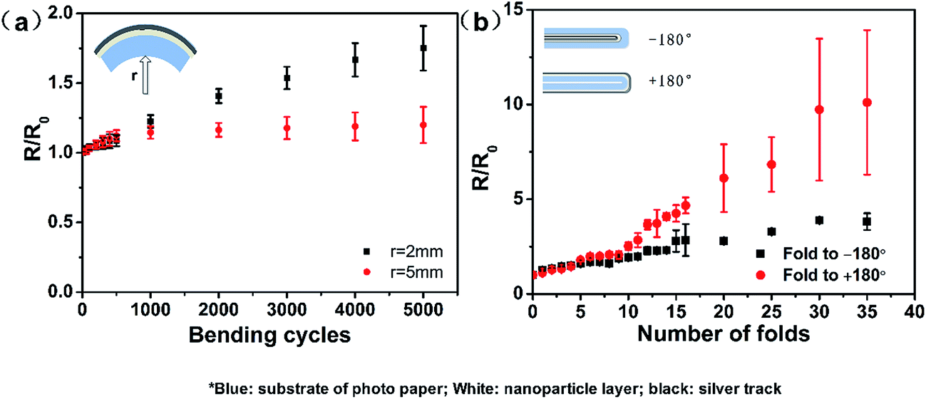 | ||
| Fig. 8 (a) The R/R0 as a function of bending cycles and the bending radii and (b) the R/R0 as a function of fold angles and number of folds. | ||
We also investigated the electrical response further to consider the most extreme folded states, in which the test specimen was folded to −180° (with silver tracks on its inner surface), released back to 0° or folded to +180° (with silver tracks on the outer surface), and then released back to 0°. The change in the electrical resistance of silver tracks as a function of the number of folds is shown in Fig. 8b. The conductive tracks on the photo paper substrate did not fully break after folding to −180° for 35 cycles (as shown in Fig. S4d†). When folded to −180° for 37 cycles, two tracks underwent full breakage and completely failed to respond in the following cycle. However, when folded to +180° for 35 cycles, the resistance increased by 14 times, as shown in Fig. S4e.† In the following 10 cycles, the tracks were still conductive although the resistance still increased. After another 10 cycles, the tracks were fully broken, as shown in Fig. S4f.† The electrical resistance of the drawn silver tracks gradually increased with the repeated folding of the test specimens. The optical images confirmed that the increase in electrical resistance resulted from the cracks formed in the conductive track at the point of folding. These formations of cracks occurred upon repeated folding, which caused the breaking of the 3D-network and the breaking of the contacts between silver particles.
The adhesion of the tracks on the photo paper was measured by a tape test according to ASTM-3359B, and the adhesion rating was 5B, where the edges were completely smooth and none of the squares of the lattice were detached, which was very important for practical applications.
A rapidly growing range of applications requires electronic systems that cannot be reached in a conventional manner on semiconductor wafers. For example, twistable electronics, which have performance equal to that of the established technologies that use a rigid wafer, have wide applications in flexible devices. Herein, we drew a simple pattern on the photo paper using the fabricated conductive pen and attached some LED units, as shown in Fig. 9. The drawn circuit showed excellent electrical conductivity, and the brightness did not deteriorate even when it was twisted.
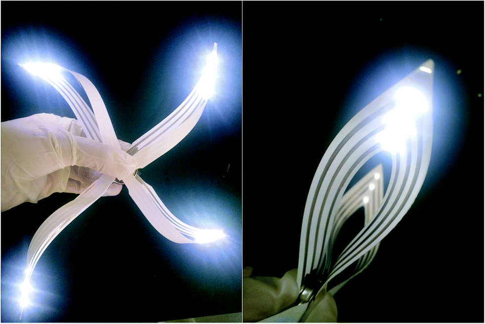 | ||
| Fig. 9 The performance of the LEDs on the photo paper with the circuits drawn by the conductive pen. | ||
4. Conclusions
In this study, we developed a large-scale and facile synthesis of silver nanoparticles by a microwave method and widened the synthetic process window for the uniform silver nanoparticles with a size less than 20 nm. The obtained silver nanoparticles could be uniformly dispersed in water and used to make conductive ink to draw conductive tracks on the photo paper without heat treatment. These tracks exhibited a good electrical conductivity of 2.4 μΩ cm, which was about 1.5 times that of the bulk silver. Via rigorous analysis and testing, we concluded that the rapid realization of conductivity at room temperature was attributed to the chemical sintering of silver nanoparticles on the surface of the substrate. The tracks on the photo paper showed good adhesiveness and mechanical stability. After bending at a radius of 4 mm and 2 mm for 5000 circles, only a slight increase in their resistance of 1.20 and 1.78 relative to their initial resistance, respectively, was observed. The as-prepared conductive pen has potential applications in flexible electronics such as LEDs, flexible sensors, and DIY activities. Therefore, this research could promote the industrialization of applications to some extent based on silver nanoparticles.Acknowledgements
This work was supported by the Science and Technology Commission of Shanghai Municipality (13DZ2296000) and Natural Science Foundation of Shanghai (16ZR1410700).References
- Z. Zhang, X. Zhang, Z. Xin, M. Deng, Y. Wen and Y. Song, Nanotechnology, 2011, 22, 425601 CrossRef PubMed.
- S. Q. Kong Liu, X. Zhang, F. Tan and Z. Wang, Nanoscale Res. Lett., 2013, 8, 88–93 CrossRef PubMed.
- C.-Y. Cho, S.-H. Hong and S.-J. Park, Thin Solid Films, 2015, 590, 76–79 CrossRef CAS.
- H. Guo, B. Xing, J. C. White, A. Mukherjee and L. He, Analyst, 2016, 141, 5261–5264 RSC.
- L. Polavarapu, A. L. Porta, S. M. Novikov, M. Coronado-Puchau and L. M. Liz-Marzan, Small, 2014, 10, 3065–3071 CrossRef CAS PubMed.
- H. L. Gomes, M. C. R. Medeiros, F. Villani, J. Canudo, F. Loffredo, R. Miscioscia, C. Martinez-Domingo, E. Ramon, E. Sowade, K. Y. Mitra, R. R. Baumann, I. McCulloch and J. Carrabina, Microelectron. Reliab., 2015, 55, 1192–1195 CrossRef CAS.
- T. Syrový, T. Kazda, L. Syrová, J. Vondrák, L. Kubáč and M. Sedlaříková, J. Power Sources, 2016, 309, 192–201 CrossRef.
- M. D. Steinberg, P. Kassal and I. M. Steinberg, Electroanalysis, 2016, 28, 1149–1169 CrossRef CAS.
- K. K. Adhikari, Y. Jung, H. Park, G. Cho and N.-Y. Kim, J. Nanomater., 2015, 2015, 1–8 Search PubMed.
- R. Ashayer-Soltani, C. Hunt and O. Thomas, Text. Res. J., 2015, 86, 1041–1049 CrossRef.
- W. Yang, C. Liu, Z. Zhang, Y. Liu and S. Nie, J. Mater. Sci.: Mater. Electron., 2012, 24, 628–634 CrossRef.
- N. Zhang, J. Luo, R. Liu and X. Liu, RSC Adv., 2016, 6, 83720–83729 RSC.
- M. Zhang, Q. Deng, L. Shi, A. Cao, H. Pang and S. Hu, Optik, 2016, 127, 145–147 CrossRef CAS.
- C. Jiang, L. Li and P. W. T. Pong, RSC Adv., 2015, 5, 98747–98756 RSC.
- C. Florian, F. Caballero-Lucas, J. M. Fernández-Pradas, R. Artigas, S. Ogier, D. Karnakis and P. Serra, Appl. Surf. Sci., 2015, 336, 304–308 CrossRef CAS.
- T. Donnelly and J. G. Lunney, Appl. Surf. Sci., 2013, 282, 133–137 CrossRef CAS.
- I. Theodorakos, F. Zacharatos, R. Geremia, D. Karnakis and I. Zergioti, Appl. Surf. Sci., 2015, 336, 157–162 CrossRef CAS.
- K. M. M. Abou El-Nour, A. a. Eftaiha, A. Al-Warthan and R. A. A. Ammar, Arabian J. Chem., 2010, 3, 135–140 CrossRef CAS.
- P. Logeswari, S. Silambarasan and J. Abraham, J. Saudi Chem. Soc., 2015, 19, 311–317 CrossRef.
- N. G. Bastús, F. Merkoçi, J. Piella and V. Puntes, Chem. Mater., 2014, 26, 2836–2846 CrossRef.
- R. I.-P. Ericka Rodríguez-León, R. Elena Navarro, R. Herrera-Urbina, J. Tánori, C. Iñiguez-Palomares and A. Maldonado, Nanoscale Res. Lett., 2013, 8, 318–326 CrossRef PubMed.
- H. Peng, A. Yang and J. Xiong, Carbohydr. Polym., 2013, 91, 348–355 CrossRef CAS PubMed.
- Y. Xia, Y. Xiong, B. Lim and S. E. Skrabalak, Angew. Chem., 2009, 48, 60–103 CrossRef CAS PubMed.
- J. Ærøe Hyllested, M. Espina Palanco, N. Hagen, K. B. Mogensen and K. Kneipp, Beilstein J. Nanotechnol., 2015, 6, 293–299 CrossRef PubMed.
- J. Niittynen, R. Abbel, M. Mäntysalo, J. Perelaer, U. S. Schubert and D. Lupo, Thin Solid Films, 2014, 556, 452–459 CrossRef CAS.
- S. Wünscher, S. Stumpf, J. Perelaer and U. S. Schubert, J. Mater. Chem. C, 2014, 2, 1642 RSC.
- S. Ma, V. Bromberg, L. Liu, F. D. Egitto, P. R. Chiarot and T. J. Singler, Appl. Surf. Sci., 2014, 293, 207–215 CrossRef CAS.
- A. Albrecht, A. Rivadeneyra, A. Abdellah, P. Lugli and J. F. Salmerón, J. Mater. Chem. C, 2016, 4, 3546–3554 RSC.
- Y. Jo, S.-J. Oh, S. S. Lee, Y.-H. Seo, B.-H. Ryu, J. Moon, Y. Choi and S. Jeong, J. Mater. Chem. C, 2014, 2, 9746–9753 RSC.
- J. H. Choi, K. Ryu, K. Park and S.-J. Moon, Int. J. Heat Mass Transfer, 2015, 85, 904–909 CrossRef CAS.
- G. Qin and A. Watanabe, J. Nanopart. Res., 2014, 16, 2684–2695 CrossRef.
- I.-s. Lee, K. Ryu, K.-H. Park, Y.-J. Moon, J.-Y. Hwang and S.-J. Moon, Int. J. Heat Mass Transfer, 2017, 108, 1960–1968 CrossRef CAS.
- J. Perelaer, B. J. de Gans and U. S. Schubert, Adv. Mater., 2006, 18, 2101–2104 CrossRef CAS.
- W. V. Werner Zapka, C. Loderer and P. Lang, in NIP24 and Digital Fabrication Järfälla, Sweden, 2008 Search PubMed.
- M. G. Shlomo Magdassi, O. Berezin and A. Kamyshny, ACS Nano, 2010, 4, 6 Search PubMed.
- A. K. Michael Grouchko, C. F. Mihailescu, D. F. Anghel and S. Magdassi, ACS Nano, 2011, 5, 6 Search PubMed.
- M. G. Shlomo Magdassi, O. Berezin and A. Kamyshny, ACS Nano, 2010, 4, 1943–1948 CrossRef PubMed.
- . Werner Zapka and C. Loderer, in NIP24 and Digital Fabrication 2008, Pittsburgh, PA, 2008 Search PubMed.
- V. K. LaMer and R. H. Dinegar, J. Am. Chem. Soc., 1950, 72, 4847–4854 CrossRef CAS.
- G. A. Tompsett, W. C. Conner and K. S. Yngvesson, ChemPhysChem, 2006, 7, 296–319 CrossRef CAS PubMed.
- W. Y. Xiaochun Xu, J. Liu and L. Lin, Sep. Purif. Technol., 2001, 25, 9 Search PubMed.
- E. V. S. Holger Borchert, A. Robert, I. Mekis, A. Kornowski, G. Gru bel and H. Weller, Langmuir, 2005, 21, 1931 CrossRef PubMed.
- R. Ma, C. Levard, S. M. Marinakos, Y. Cheng, J. Liu, F. M. Michel, G. E. Brown and G. V. Lowry, Environ. Sci. Technol., 2012, 46, 752–759 CrossRef CAS PubMed.
- W. Li, M. Chen, W. Li, C. You, J. Wei and L. Zhi, Mater. Res. Innovations, 2014, 18, S4-723–S4-727 CrossRef.
- Y.-L. Tai and Z.-G. Yang, J. Mater. Chem., 2011, 21, 5938–5943 RSC.
- A. K. Michael Grouchko, C. F. Mihailescu, D. Florin Anghel and S. Magdassi, ACS Nano, 2011, 5, 3354–3359 CrossRef PubMed.
- M. Ernstsson, O. J. Rojas, R. D. Neuman and P. M. Claesson, Langmuir, 2002, 18, 1604–1612 CrossRef.
Footnote |
| † Electronic supplementary information (ESI) available. See DOI: 10.1039/c7ra05125e |
| This journal is © The Royal Society of Chemistry 2017 |