
 Open Access Article
 This Open Access Article is licensed under a
 Creative Commons Attribution 3.0 Unported Licence
Structure-property relationships for Eu doped TiO2 thin films grown by a laser assisted technique from colloidal sols
I. Campsa,
M. Borlaf†
b,
M. T. Colomerb,
R. Morenob,
L. Dutac,
C. Nitac,
A. Perez del Pinod,
C. Logofatue,
R. Sernaa and
E. György *cd
*cd
aInstituto de Óptica, Consejo Superior de Investigaciones Científicas (CSIC), C/Serrano 121, 28006 Madrid, Spain
bInstituto de Cerámica y Vidrio, Consejo Superior de Investigaciones Científicas (CSIC), C/Kelsen 5, 28049, Madrid, Spain
cNational Institute for Lasers, Plasma and Radiation Physics, PO Box MG 36, 077125 Bucharest V, Magurele, Romania
dInstituto de Ciencia de Materiales de Barcelona, Consejo Superior de Investigaciones Científicas (ICMAB-CSIC), Campus UAB, 08193 Bellaterra, Spain. E-mail: egyorgy@icmab.es; Fax: +34 935805729; Tel: +34 935801853
eNational Institute for Materials Physics, P. O. Box MG 7, 077125 Bucharest V, Magurele, Romania
First published on 31st July 2017
Abstract
Photoactive europium doped titanium dioxide (Eu:TiO2) thin films were grown by a matrix assisted pulsed laser evaporation technique. TiO2 and Eu cation-adsorbed TiO2 nanoparticles (NPs) sols were used as starting materials. The sols were synthesized by a colloidal sol–gel route. In order to obtain solid targets, the sols were cooled down until solidification in liquid nitrogen. The irradiation of the solid targets was performed in a controlled oxygen atmosphere using an UV KrF* (λ = 248 nm, τFWHM ≤ 25 ns, ν = 10 Hz) excimer laser source. The NPs were transferred and deposited onto solid substrates placed in the front of the frozen targets, forming continuous thin films. The as-grown undoped and Eu:TiO2 thin films were submitted to post-deposition thermal treatments. The surface morphology, crystalline structure, and chemical composition of the thin films were characterized by field emission scanning electron microscopy, X-ray diffraction, and X-ray photoelectron spectroscopy. Functional optical properties of the films were investigated by UV-VIS-NIR spectroscopy, spectroscopic ellipsometry, and photoluminescence as a function of dopant concentration in the TiO2 host and annealing temperature. A direct correlation was established between the processing conditions, films structure, chemical composition and oxidation states studied both at the top surface and in-depth as well as their functional, optical properties. Eu doping induces a blue-shift of the absorption edge with respect to the as-grown samples. Under visible light excitation (λ = 488 nm, emitted by an Ar+ laser source), the Eu:TiO2 samples show characteristic photoluminescence corresponding to the 5D0 → 7Fi (i = 0, 1, 2, 3, 4) transitions of Eu+ ions in the visible spectral range. The samples treated at the highest annealing temperature are characterized by strong photoluminescence emission, high transmittance in the VIS-NIR spectral regions, and high refractive index.
1. Introduction
Titanium dioxide (TiO2) is a wide band-gap semiconductor, which has been intensively investigated during the few last years due to its exceptional properties such as high hardness, corrosion resistance, non-toxicity, bio- and chemical inertness, mechanical stability, high resistance to photo-induced decomposition, high light-conversion efficiency, and low cost.1 Its practical applications include solar and electrochemical cells, gas sensors, optical waveguides, bio-medical products, or photocatalysts for polluted water and air treatment, by the degradation of organic compounds.2–5 Lanthanide ions doped semiconductor metal oxide nanoparticles (NPs) are investigated for optoelectronic applications, including phosphors for lighting, flat panel displays, lasers, markers in biology, optical amplifiers, or solar cells.6–10 Moreover, it was reported that lanthanide ions improve the photocatalytic efficiency of TiO2 due to band gap reduction.11–13 Among lanthanide ions, Eu3+ is one of the most studied, due to its sharp emission band in the visible spectral region, attributed to the 5D0 → 7Fi (i = 0, 1, 2, 3, 4) transitions.9,10For most of the industrial applications colloidal NPs obtained by solution-based chemical methods must be immobilized onto solid substrates in form of highly adherent structures or thin films. Different deposition procedures are currently used to this purpose, as doctor-blading, dip-coating, or screen-printing.14,15 However, these techniques in most cases do not lead to the growth of continuous thin films with uniform thicknesses across the deposited area. Moreover, they do not allow for a precise control of the thickness of the deposited layers. These are serious inconveniences which hamper the integration of the films in optical and optoelectronic devices. In this work the growth through laser techniques of Eu:TiO2 thin films from aqueous Eu cations-adsorbed TiO2 nanoparticulate sols is reported. Owing to numerous advantages, laser-based deposition methods could become an alternative to conventional deposition methods. Among them stands the short processing time, control of the quantity of the transferred material through the number of the subsequent laser pulses applied for the irradiation of the targets, multilayer synthesis avoiding solvent incompatibilities, and good adherence of the layers.16 Additionally, our previous results revealed that the films' chemical composition and stoichiometry, and thus their functional, optical, electric, and catalytic properties can be easily adjusted through the MAPLE process parameters as the pressure as well as nature of the reactive gases in the irradiation chamber.17–20 Moreover, in contracts to solvent-based chemical methods, laser technologies allow for the development of composites and multilayers bearing simultaneously various functionalities, as e.g. optical, catalytic, or magnetic properties.
We used in our experiments the technique called matrix assisted pulsed laser evaporation (MAPLE), initially developed for organic and bio-organic materials processing.21,22 The technique is until certain extent similar to the conventional pulsed laser deposition (PLD), commonly used for inorganic thin films growth. The difference between the two MAPLE and PLD is that in MAPLE the target is a dispersion which contains the material of interest which will be transferred to the substrate surface. The dispersions are cooled down until solidification in liquid nitrogen, similarly to conventional PLD targets. More recently, besides organic materials, the transfer by MAPLE technique of nano-entities as carbon and carbon/gold NPs composites23,24 SnO2 NPs,25 CdSe/ZnS core–shell quantum dots,26 TiO2 nanorods,27 single- and multiwall carbon nanotubes,21,28,29 single- and multiwall carbon nanotubes/polymer composites,30,31 graphene oxide (GO),17 TiO2 NPs/GO composites,18,19 or TiO2/GO/Au ternary compounds20 was reported. In these works, the target dispersions were irradiated by laser sources emitting in the UV spectral range. As solvent for the preparation of the target dispersions toluene, acetone, dimethyl sulfoxide, dimethyl formamide, methanol, or ethyl acetate was used, with high absorption at the wavelength of the incident UV laser radiation.17,27–31 Distilled water, transparent to the UV laser radiation was also used as solvent matrix for the preparation of targets, avoiding health and environmental hazards typical for organic solvents.18–20
In the present work the laser induced transfer of TiO2 and Eu:TiO2 NPs onto solid substrates by MAPLE technique using aqueous Eu cations-adsorbed TiO2 NPs colloids as starting materials is reported. Our aim was to obtain uniform and continuous Eu doped TiO2 thin films, suitable for a large variety of optical applications, as photocatalysis, dye-sensitized solar cells, color displays, optical sensors, or nanoscaled optoelectronic devices.32–34
The aqueous Eu cations-adsorbed TiO2 NPs sols were obtained by a colloidal sol–gel route.35 The as-grown thin films were submitted to post-deposition thermal treatments. The objective of this work was to establish a correlation between the structure and chemical composition of the Eu doped TiO2 layers with their optical properties, as function of Eu dopant concentration in the TiO2 host material and post-deposition annealing temperature. The chemical composition and Eu oxidation state was investigated both at the top surface of the layers as well as in-depth. The mechanisms of the photoluminescence emissions in the visible spectral range, along with structural changes induced by annealing and Eu dopant incorporation into the TiO2 host, are discussed. We demonstrate that the optical transparency and photoluminescence properties of the layers, key parameters for practical applications, can be modulated through the annealing temperature and Eu dopant concentration.
2. Experimental
Undoped and Eu cations-adsorbed TiO2 NPs sols were produced using a colloidal sol–gel route, according to the procedure reported previously.35 For the preparation of the sols titanium(IV) isopropoxide (97% Sigma-Aldrich, Steinheim, Germany) was added to a stirring mixture of deionized water (18.2 MΩ cm−1, ultrapure Milli-Q) and nitric acid (Merck, Darmstadt, Germany) in a water![[thin space (1/6-em)]](https://www.rsc.org/images/entities/char_2009.gif) :alkoxide molar ratio of 50:1 solution. In TiO2/Eu3+ sols, before the addition of the alkoxide, europium(III) acetate hydrate [Eu(OOCCH3)3·xH2O, Sigma-Aldrich, Steinheim, Germany] was dissolved in the mixture of water and nitric acid to a molar ratio Eu3+/TiO2 of 1, 2, and 3%, respectively. The synthesis temperature was maintained constant during the entire process at 35 °C. HNO3 (65%, PANREAC, Barcelona, Spain) was used as a catalyst in a molar ratio H+/Ti4+ of 0.2.
:alkoxide molar ratio of 50:1 solution. In TiO2/Eu3+ sols, before the addition of the alkoxide, europium(III) acetate hydrate [Eu(OOCCH3)3·xH2O, Sigma-Aldrich, Steinheim, Germany] was dissolved in the mixture of water and nitric acid to a molar ratio Eu3+/TiO2 of 1, 2, and 3%, respectively. The synthesis temperature was maintained constant during the entire process at 35 °C. HNO3 (65%, PANREAC, Barcelona, Spain) was used as a catalyst in a molar ratio H+/Ti4+ of 0.2.
The obtained NPs sols were used for the preparation of the MAPLE targets. The sold were placed a special double wall target holder and flash-frozen circulating liquid nitrogen between the walls. The targets were kept frozen during the experiments. A pulsed UV KrF* (λ = 248 nm, τFWHM ≤ 25 ns, ν = 10 Hz) COMPexPro 205 Lambda Physik excimer laser source was used for the irradiation of the frozen targets. The experiments were performed inside a stainless steel deposition chamber. Prior to each experiment, the chamber was evacuated down to a residual pressure of 10−3 Pa. And then filled with O2 at 20 Pa pressure. The targets were rotated with a frequency of 3 Hz, with the aim to avoid significant changes in their surface morphology induced by the laser radiation. The incidence angle of the laser beam onto the target surface was of 45°. 2000 subsequent laser pulses were applied for the deposition of each sample. The laser fluence value on the target's surface was fixed at 0.4 J cm−2. Si (100) and SiO2 fused silica plates with 1 × 1 cm2 surface area were used as substrates. The substrates were cleaned in ultrasonic bath with acetone and ethanol and placed plan-parallel to the target surface at a separation distance of 4 cm. During the laser deposition process, the substrates were heated at 50 °C. The as-grown films were submitted to thermal annealing for 1 h in air at atmospheric pressure at temperature values of 300, 400, and 500 °C, respectively.
The surface morphology of the layers was investigated by field emission scanning electron microscopy (FE-SEM) with a QUANTA FEI 200 FEG-ESEM system. Their crystalline structure was investigated by X-ray diffraction (XRD) by means of a Bragg–Brentano Rigaku Rotaflex RU-200BV diffractometer in θ–2θ configuration with a step of 0.02°. The Cu Kα radiation (1.5418 Å) was chosen for excitation. S-ray photoelectron spectroscopy (XPS) studies were performed to obtain information about the chemical bonds between the elements both at the top surface as well as in-depth through Ar+ sputtering, with the aid of a SPECS XPS spectrometer, based on Phoibos 150 electron energy analyzer operated in constant energy mode. The instrument work function was calibrated to give a binding energy of 84 eV for the Au 4f7/2 line of metallic gold. A monochromatic X-ray source, Al Kα (1486.74 eV) was used for excitation. The measurements were performed at 10−7 Pa residual pressure. High resolution spectra were acquired over smaller ranges of 20 eV using 0.05 eV step at 10 eV pass energy and energy resolution of 0.7 eV (FWHM of the Au 4f7/2 line). The obtained data were analyzed using SDPXPS software (version 7.0).
Optical transmission and reflection spectra of the samples were registered with the aid of a Varian Cary 5000 UV-VIS-NIR spectrophotometer. Spectroscopic ellipsometry measurements were carried out in the 550–1700 nm (0.73–2.55 eV) wavelength range at incidence angles of 65°, 70° and 75° using a VASE ellipsometer (J. A. Woollam Co., Inc.) in order to determine the dielectric function of the films and thickness. The ellipsometric Ψ and Δ values have been fitted to obtain the complex refractive index n = n + ik using a Cauchy function for the real part of the refractive index (n) and an Urbach absorption tail for the imaginary part of the refractive index (k) values. Photoluminescence measurements were performed using an Ar+ ion laser source (Spectra-Physics 2020-03) at 488 nm excitation wavelength and nominal power of 200 mW. The light emitted by the samples was collected with a Czerny–Turner type monochromator (Acton Spectra Pro300i, with a diffraction grating of 1200 g mm−1 for the visible range) and detected through a photomultiplier (EMI 9659QB-S20). The signal was amplified through the standard lock-in technique.
3. Results and discussion
3.1. Surface morphology
The FE-SEM images of as-grown undoped and Eu doped TiO2 layers are presented in Fig. 1. The surface morphology of the undoped (Fig. 1a, b and d) and Eu doped layers (Fig. 1c, e and f) is very similar, as can be observed in images Fig. 1b and c, and does not change significantly after the post-deposition thermal annealing process (Fig. 1e and f). The layers are constituted by irregular-shaped aggregates and spherical particles with size ranging from a few tens of nm up to hundreds of nm, uniformly distributed over the substrate surface. The high resolution FE-SEM images disclosed further topographical details concerning the structure of the layers (Fig. 1d–f). The irregular-shaped aggregates are formed by nanoparticles with sizes of tens and below tens of nm. The small, nano-sized particles are covering also the surface of part of the large, hundreds of nm sized spherical particles (Fig. 1f). | ||
| Fig. 1 FE-SEM image of as-grown (a and b) undoped TiO2 thin film and (c) Eu:TiO2 thin film obtained from 3% Eu3+/TiO2 molar ratio colloidal sols TiO2 thin film. High resolution FE-SEM image of as-grown (d) undoped TiO2 thin film and Eu:TiO2 thin film obtained from 3% Eu3+/TiO2 molar ratio colloidal sols (e) before and (f) after thermal treatment at 500 °C. | ||
According to previous transmission electron microscopy analyses, the diameters in the sols of the initial TiO2 and Eu cations adsorbed TiO2 NPs which were further used as targets in the MAPLE experiments were around 5 nm.35 The larger size and spherical shape of the particles deposited on the substrate surface indicate that the temperature of the initial TiO2 NPs during the laser irradiation exceeded the melting temperature, and the particles are formed in liquid phase by coalescence. Indeed, the melting threshold of TiO2 films irradiated by an UV KrF* excimer laser was found to be around 0.25 J cm−2,36 below the laser fluence value used during MAPLE, 0.40 J cm−2. Moreover, our numerical simulations of the temperature evolution of TiO2 NPs during laser irradiation showed that the NPs undergo a rapid heating process, with heating rates of the order of 1010–1011 K s−1.19 Thus, the NPs act as absorption centers, increasing the temperature of the water matrix by heat transfer leading to sublimation and vaporization. The water matrix is transparent to the wavelength of the incident laser radiation, consequently direct heating cannot take place. On the other hand, the water matrix surrounding the TiO2 NPs can be superheated37 through rapid heating process induced by the laser radiation, reaching its spinodal temperature, leading to explosive boiling. The individual particles and aggregates can be transported from the targets towards the substrate surface by the water droplets produced in the explosive boiling process.
3.2. Crystalline structure
The initial sols consist of tetragonal anatase phase and a low amount of brookite phase TiO2 or Eu cations adsorbed TiO2 NPs.32 The X-ray diffractograms of the TiO2 and Eu:TiO2 layers, as-grown as well as after thermal treatment, are presented in Fig. 2.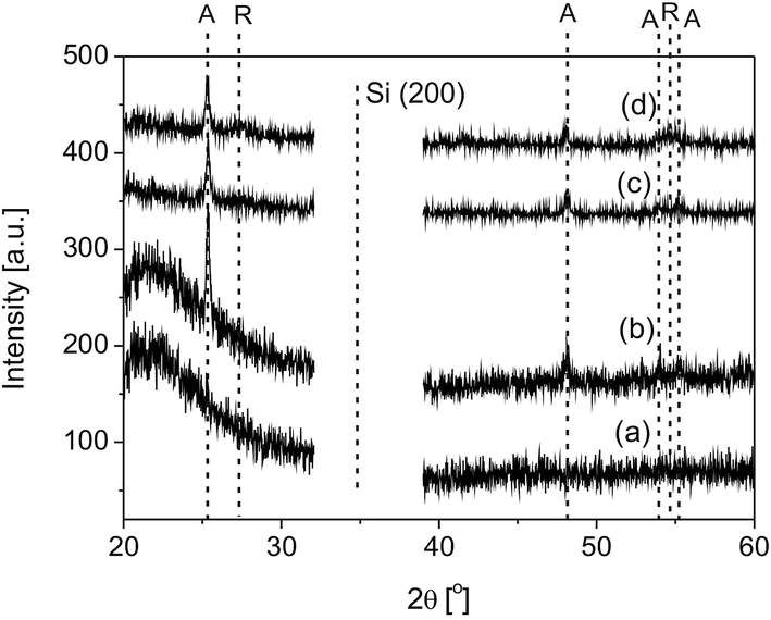 | ||
| Fig. 2 XRD patterns of TiO2 thin film (a) as-grown and (b) submitted to post-deposition thermal annealing at 500 °C for 1 h as well as Eu:TiO2 thin films obtained from (c) 1 and (d) 3% Eu3+/TiO2 molar ratio colloidal sols submitted to post-deposition thermal annealing at 500 °C for 1 h. The identifications correspond to anatase (A) and rutile (R) crystalline phases. | ||
The as-grown TiO2 and Eu:TiO2 layers are amorphous (Fig. 2a). Post-deposition thermal treatment at 500 °C for 1 h induced the crystallization of the films (Fig. 2b–d). The peaks at 25.30°, 48.04°, 53.89°, and 55.06° correspond to the (101), (200), (105), and (211) lattice plane reflections of polycrystalline tetragonal anatase phase TiO2, as referred in the JC-PDS 21-1272 file.38 The low intensity peaks at 27.44° and 54.32° indicate the presence of a reduced amount of tetragonal rutile phase TiO2, corresponding to the (110) and (211) lattice plane reflections, as referred in the JC-PDS 21-1276 file.38 The crystallization of divalent- or trivalent-europium containing oxide compounds could be not detected by XRD analysis. Similarly to these results, undoped and Eu:TiO2 sols, identical to those used as targets in the MAPLE experiments, were found to consist of a mixture of anatase and rutile crystalline phases when heating at temperatures higher than 500 °C.35 Eu doping did not lead to the shift of the diffractions peaks. This feature is in agreement with other results reported in the literature for low Eu doping levels.33,39 Due to the high mismatch in the ion radii of Eu3+ and Ti4+, 0.95 and 0.68 Å, respectively,40 substitution of Ti4+ by Eu3+ within the anatase lattice is difficult. Thus, Eu3+ ions the most probably does not occupy a crystallographic position in TiO2 and were associated to interstitial positions in the anatase crystal structure.39
The average size of the nano-crystallites constituting the films was estimated by the Scherrer analysis with the aid of the formula:41
| Dhkl = 0.9λ/βhklcosθhkl |
3.3. Chemical composition
The chemical composition and Ti and Eu oxidation states were investigated both at the top surface of the layers as well as in-depth through Ar+ sputtering. The high-resolution Ti 2p and O 1s XPS spectra of the as-grown (a) TiO2 and (b–d) Eu:TiO2 thin films, as well as (e) Eu:TiO2 thin film annealed at 500 °C for 1 h in air at atmospheric pressure are shown in Fig. 3. All spectra were registered at the top surface of the films (a and b) as well as in-depth, after 5 and 10 min Ar+ sputtering (c–e).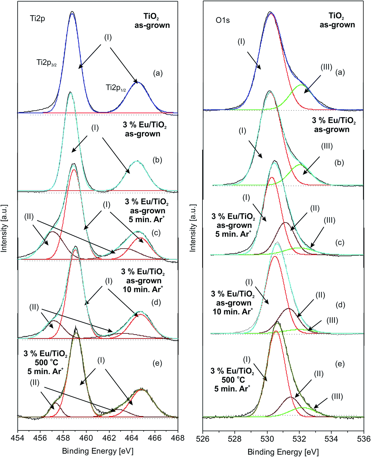 | ||
| Fig. 3 Ti 2p and O 1s XPS spectra registered at the top surface of as-grown (a) TiO2 and (b) Eu:TiO2 thin film obtained from 3% Eu3+/TiO2 molar ratio colloidal sols; in-depth of as-grown Eu:TiO2 thin film obtained from 3% Eu3+/TiO2 molar ratio colloidal sols after (c) 5 and (d) 10 min. Ar+ sputtering; (e) in depth after 5 min. Ar+ sputtering of Eu:TiO2 thin film obtained from 3% Eu3+/TiO2 molar ratio colloidal sols submitted to post-deposition thermal annealing at 500 °C for 1 h in air. | ||
The Ti 2p3/2 and Ti 2p1/2 lines of the Ti 2p spectra (lines I) of the (a) undoped and (b) Eu:TiO2 thin films registered at the top surface are centered at 458.8, and 464.6 eV, respectively, corresponding to the values reported in the literature for stoichiometric TiO2.43,44 In the spectra of the films submitted to Ar+ sputtering for (c) 5 and (d) 10 min the contribution of Ti–O bonds of titanium suboxides can be clearly distinguished (lines II). The lines are situated at binding energies around 1.5 eV lower as compared to Ti–O bonds in stoichiometric TiO2 and can be assigned to Ti–O bonds in Ti2O3.43,44 The presence of lower oxidation states could be attributed to the reduction of the initial TiO2 NPs during laser processing. As a consequence, the composition of the thin films will be different in the depth as compared to the top surface, which is fully oxidized due to air exposure.
On the other hand, it was reported that Ar+ sputtering can induce changes in the chemical states of transition metal oxides, stoichiometric oxides being reduced, resulting in additional components in the XPS spectra.45 However, the intensity of the lines was reported to increase gradually with the increase of the sputtering time during the first 15 min,45 in contrast to our results. The peak areas corresponding to Ti suboxides normalized to the total Ti 2p peak area are presented in Fig. 4a.
 | ||
| Fig. 4 (a) Ti suboxides XPS peak areas normalized to the total Ti 2p spectra and (b) Eu3+ peak area normalized to the total Eu 3d5/2 spectra. | ||
The AII/(AI + AII) ratio calculated for the spectrum registered after 10 min Ar+ ion sputtering remains below that registered after 5 min sputtering. As a consequence, even if Ar+ sputtering can contribute to the changes of chemical states, titanium suboxides could be present besides stoichiometric TiO2 in the composition of the as-grown films. Moreover, the intensity of the lines corresponding to Ti suboxides are lower in case of the thermally treated samples submitted to Ar+ sputtering (Fig. 3e) as compared to the as-grown counterpart (Fig. 3c) indicating that oxidation of the sample takes place during post-deposition annealing. Similarly, the peak area of suboxides normalized to the total Ti content of the thermally treated sample is significantly lower as compared to the as-grown sample.
The O 1s spectra registered at the top surface of the undoped (a) and Eu:TiO2 films (b) were deconvoluted in two lines (Fig. 3). The main line centered at 530.2 eV (line I) is attributed to Ti–O bonds in the stoichiometric TiO2 structure.43,44 Eu–O bonds can contribute to the main line in case of the Eu:TiO2 thin film since their binding energy value coincide with that of the Ti–O bonds of TiO2.46 The smaller peak situated at 532.3 eV (line III) can be assigned to H–O bonds of hydroxyl groups from chemically adsorbed H2O molecules on the surface of the thin films.47 The intensity of the line diminishes gradually in the depth of the TiO2 with the increase of the Ar+ sputtering time (c and d). Moreover, the line (II) in the spectra registered after Ar+ sputtering (c–e) can be assigned to Ti suboxides, in accordance with the corresponding Ti 2p spectra.
The Eu 4d spectrum of the Eu:TiO2 film registered at the top surface (Fig. 5a) is composed of four peaks, corresponding to two different valence states (2+ and 3+) of Eu ions in the TiO2 host. Both valence states are doublets, Eu 4d5/2 and Eu 4d3/2 and are centered at 128.3 and 133.6 eV for Eu2+ (lines I), and at 136.4 and 141.5 eV for Eu3+ (lines II).46–48 Similarly, the Eu 3d5/2 spectrum of the film (Fig. 5a) contains contributions from both the Eu2+ and Eu3+ ions, situated at 1125.1 eV (line I) and 1134.7 eV (line II), respectively.46 Both the Eu 4d and Eu 3d5/2 spectra indicate that the relative contribution of the Eu3+ as compared to the Eu2+ state is more significant, the Eu3+/Eu2+ ratio calculated from the integrated peak areas of the Eu 3d5/2 line being around 1.5. The co-existence of bivalent and trivalent contributions could be attributed to the different environments on the surface as compared to the bulk, called “surface valence transitions”, resulting in the formation of higher oxidation states, or to the formation of mixed valence states during the films growth process.49 The Eu 4d and Eu 3d5/2 spectra recorded in depth after 5 (Fig. 5b) and 10 min (Fig. 5c) Ar+ sputtering are completely different as compared to the top surface, the Eu2+ contribution being dominant over Eu3+. The spectra do not change significantly with the increase of the sputtering time indicating that the presence of lower oxidation states cannot be attributed entirely to the Ar+ sputtering process.
 | ||
| Fig. 5 Eu 4d and Eu 3d5/2 XPS spectra of as-grown Eu:TiO2 thin film obtained from 3% Eu3+/TiO2 molar ratio colloidal sols registered (a) at the top surface and in-depth after (b) 5 and (c) 10 min Ar+ sputtering; Eu:TiO2 thin film obtained from 3% Eu3+/TiO2 molar ratio colloidal sols submitted to post-deposition thermal annealing at 500 °C for 1 h in air registered at (d) the top surface and (e) in depth after 5 min. Ar+ sputtering. | ||
The quantification of the peak areas AII corresponding to Eu3+ normalized to the Eu 3d5/2 AI + AII peak areas, shows that the Eu3+ content of the samples is slightly below after 10 as compared to 5 min Ar+ sputtering (Fig. 4b). Very similar results were reported in the scientific literature for Eu oxide nano-layers coated on TiO2 particles49 and Eu implanted SrTiO3 single crystals,47 submitted to Ar+ sputtering. Thus, the reduction processes induced by Ar+ sputtering could contribute to the formation of additional Eu2+ states.
After thermal treatment performed at 500 °C in air, the relative intensities and total areas of the lines corresponding to the Eu3+ ions increase as compared to those of the Eu2+ ions, both in case of the Eu 4d as well as Eu 3d5/2 spectra registered at the top surface of the sample (Fig. 5d). Indeed, an Eu3+/Eu2+ ratio of around 2.4 was calculated from the integrated peak areas of the Eu 3d5/2 line, significantly higher than the value of the same sample before thermal annealing. These features indicate that oxidation from Eu2+ to Eu3+ takes place on the surface of the films during the annealing process. After 5 min Ar+ sputtering, the relative contribution of the lines corresponding to the Eu2+ state become preponderant (Fig. 5e), similarly to the spectra recorded below the top surface in case of the as-grown samples (Fig. 4b). However, the peak areas AII corresponding to Eu3+ normalized to the total Eu 3d5/2 peak areas, AI + AII, was higher in case of the annealed as compared to the as-grown sample (Fig. 4b).
3.4. Optical properties
 | ||
| Fig. 6 UV-VIS-NIR transmission spectra of TiO2 thin films, as-grown and thermally treated at 300, 400, and 500 °C. The inset shows photographs of the samples before and after thermal treatment. | ||
The UV-VIS reflection spectra of the as-grown and thermally treated pure and Eu:TiO2 thin films are shown in Fig. 7a. The reflectance in the visible spectral range of all samples increases after thermal annealing at 500 °C with around 20% for the Eu doped samples and around 50% in case of the pure TiO2 films.
 | ||
| Fig. 7 (a) UV-VIS reflection spectra of TiO2 and Eu:TiO2 thin films as-grown and thermally treated at 300, 400, and 500 °C; (b) [F(R) × hν]1/2 versus hν curves of the TiO2 and Eu:TiO2 thin films thermally treated at 500 °C. | ||
In order to obtain further information concerning the absorption edge of the samples, the Kubelka–Munk function, F(R) was calculated:50
| F(R) = (1 − R)2/(2R) | (1) |
The calculated band gap value for the undoped TiO2 sample submitted to thermal treatment at 500 °C was found to be about 3.1 eV (Fig. 7b), similar to the values reported in the literature for anatase phase TiO2.51 In contrast, rutile belongs to the direct band gap semiconductor metal oxides category. Its indirect band gap is very similar to its direct band gap, reported at around 3.0 eV.52,53 However, the dominant crystal phase in our samples was anatase TiO2 with a very low amount of rutile TiO2 (Fig. 2b–d).
Lower band gap values were calculated for the Eu doped samples as compared to pure TiO2, around 2.7 eV. Interstitial Eu doping was reported to produce lattice deformations and formation of vacancies, leading the most probably to impurity states in the band gap of TiO2.54 The effect of rare earth elements doping of TiO2 was investigated by theoretical first-principles density functional calculations in (ref. 55–57). It was found that Eu doping leads to band gap reduction of TiO2, due to the formation of impurity energy levels and new energy states inside the band gap of TiO2 leading to band gap narrowing, in good agreement with our results. Furthermore, the presence of rare earth elements influences the positions and widths, as well as the density of states of both the conduction and valence bands of TiO2.55–57
 | ||
| Fig. 8 Calculated refractive index values as a function of wavelength for the as-grown and annealed Eu:TiO2 thin films obtained from 1% Eu3+/TiO2 molar ratio colloidal sols. | ||
The increase of the refractive index at 550 nm to around 1.91 after thermal treatment can be attributed to the densification and crystallization of the layers and formation of anatase phase TiO2, as indicated by XRD results (Fig. 2). The refractive index in the 550–1700 nm spectral range is similar or still slightly below the values reported in the literature for crystalline TiO2 thin films,59–62 or bulk anatase TiO2.63 The observed increase of the diffuse reflectance (Fig. 7a) might indicate that densification and crystallization of MAPLE deposited thin films is not complete after annealing at 500 °C. Indeed, refractive index values around 2 at 550 nm wavelength were reported for samples annealed at temperatures between 300 and 450 °C.59,61 In contrast, higher refractive index values, of around 2.3, were reported for TiO2 thin films grown by atomic layer deposition.62 Post-deposition annealing lead to the formation of anatase phase TiO2 layers with refractive index values around 2.45 for the highest, 600 °C annealing temperature.62
 | ||
| Fig. 9 (a) Photoluminescence spectra of the Eu:TiO2 thin film obtained from 1, 2, and 3% Eu3+/TiO2 molar ratio colloidal sols, as-grown, and submitted to thermal treatment at 300 and 500 °C; (b) ratio of the peaks areas of the 5D0 → 7F1 and 5D0 → 7F2 transitions. | ||
It is well known that the 5D0 → 7F2 transition is an electrically allowed transition (electronic dipole transitions), and it is very sensitive to the surroundings of the Eu3+ ions.67 On the contrary, 5D0 → 7F1 transition is magnetically allowed (magnetic dipole transitions) and is almost not influenced by the surrounding TiO2 host.64 Consequently, the ratio of 5D0 → 7F2 and 5D0 → 7F1 emission lines areas provides information concerning the TiO2 host, i.e. the surrounding defects and disorder around the Eu3+ ions.64 Thus, in order to quantify the Eu3+ photoluminescence emission, the asymmetry ratio was calculated:
| R = A2(5D0 → 7F2)/A1(5D0 → 7F1) | (2) |
After thermal treatment at 300 °C and further up to 500 °C, the intensity of the wide band emission decreases, due to the reduction of the number of defects, diminishment of the amount of Ti suboxides, and the phase transition in the TiO2 host from amorphous to crystalline, as revealed also by XRD analyses (Fig. 2a and b).65–67 The reduction of the wide band emissions is accompanied by the enhancement of the 5D0 → 7Fi allowed transitions (i = 0, 1, 2, 3, 4) of the 3+ oxidation state of Eu in good agreement with our XPS investigations. The relative intensities and total area of the lines corresponding to the Eu3+ ions increase as compared to the Eu2+ ions both in the Eu 4d as well as the Eu 3d5/2 XPS spectra (compare Fig. 5a and d). Moreover, the TiO2 nanocrystallites formed upon annealing was reported to act as sensitizers, through the absorption of the excitation energy.68–70 The absorption is followed by relaxation to defect states of TiO2 and subsequently transferred to Eu3+ ions. This effect was reported to be characteristic for semi-crystalline TiO2 matrices.65 For fully crystallized anatase TiO2 matrices, the intensity of the Eu3+ luminescence emissions was found to decrease.68 This effect could explain the slight decrease of the asymmetry ratio of the 1 mol%. Eu:TiO2 thin film annealed at 500 °C (Fig. 9b). However, higher Eu doping concentration can inhibit the crystallization process71 and thus, improve the luminescence properties. Indeed, the luminescence emission and asymmetry ratio of 2 and 3% Eu:TiO2 samples annealed at 300 and 500 °C are significantly higher as compared to those of the 1% Eu:TiO2 thin film (Fig. 9a and b). These features are in good agreement with our XRD results. The intensity of the anatase TiO2 lines decrease gradually with the increase of the Eu doping concentration in the TiO2 host material (Fig. 2b–d).
4. Conclusion
TiO2 and Eu:TiO2 thin films were prepared by MAPLE method. TiO2 NPs and Eu cations-adsorbed TiO2 NPs sols synthesized using a colloidal sol–gel route were used as starting materials. The sols were cooled down until solidification and used as targets in the MAPLE deposition process. The as-grown films were submitted to post-deposition thermal treatments at temperatures ranging from 300 to 500 °C, for 1 h in air, at atmospheric pressure. The optical properties of the films were correlated with the structure and composition studied both at the tops surface as well as in-depth, as a function of Eu doping concentration in the TiO2 host as well as annealing temperature. The thin films containing the highest Eu concentration and treated at the highest temperature are translucent in the visible spectral region, have higher refractive index and significantly improved photoluminescence emission. These features can be attributed to the oxidation reactions as well as amorphous-crystalline phase transitions which take place during the annealing process. Due to their outstanding optical performance, high transmittance in the VIS-NIR spectral regions, high refractive index, and intense luminescence, the synthesized films are suitable for integration in optoelectronic devices or as photocatalysts in environmental applications owing to their low density and significant surface roughness.Acknowledgements
The authors thank the financial support of the Executive Unit for Financing Higher Education, Research, Development and Innovation of the Romanian Ministry of Education and Scientific Research under the contract PN-III-P2-2.1-PED-2016-1043 and the Spanish Ministry of Economy and Competitiveness under the project ENE2014-56109-C3-3-R. ICMAB acknowledges financial support from the Spanish Ministry of Economy and Competitiveness, through the “Severo Ochoa” Programme for Centres of Excellence in R&D (SEV- 2015-0496). I. C. and M. B. thank the financial support of Consejo Superior de Investigaciones Científicas for PhD Grants JAE-Pre-201100578 and JAE-Pre-083.References
- D. R. Lide, Handbook of Chemistry and Physics, CRC, Boca Raton, FL, 71st edn, 1991 Search PubMed.
- J. Bai and B. Zhou, Chem. Rev., 2014, 114, 10131–10176 CrossRef CAS PubMed.
- Z. Zhang, D. F. Lu and Z. M. Qi, J. Phys. Chem. C, 2012, 116, 3342–3348 CAS.
- Q. Zhang and G. Cao, Nano Today, 2011, 6, 91–109 CrossRef CAS.
- K. Honda and A. Fujishima, Nature, 1972, 238, 37–38 CrossRef.
- W. Chen, P. Yuan, S. Zhang, Q. Sun, E. Liang and Y. Ji, Phys. B, 2012, 407, 1038–1043 CrossRef CAS.
- I. Cacciotti, A. Bianco, G. Pezzotti and G. Gusmano, Chem. Eng. J., 2011, 166, 751–764 CrossRef CAS.
- J. P. Shoffner, Anal. Chem., 1975, 47, 341–343 CrossRef CAS.
- Principles of luminescence, in Luminescent materials and applications, ed. A. H. Kitai, John Wiley & Sons, Ltd., West Sussex, England, 2008 Search PubMed.
- Scintillators, in Luminescence, ed. C. R. Ronda and A. M. Srivastava, Wiley – VCH Verlag GmbH & Co. KGaA, Weinheim, Germany, 2007 Search PubMed.
- A. Kubacka, M. Fernández-García and G. Colón, Chem. Rev., 2012, 112, 1555–1614 CrossRef CAS PubMed.
- Z. M. El-Bahy, A. A. Ismail and R. M. Mohamed, J. Hazard. Mater., 2009, 166, 138–143 CrossRef CAS PubMed.
- V. Stengl, S. Bakardjieva and N. Murafa, Mater. Chem. Phys., 2009, 114, 217–226 CrossRef CAS.
- T. Uddin, Y. Nicolas, C. Olivier and T. Toupance, Low temperature preparation routes of nanoporous semiconducting films for flexible dye-sensitized solar cells, Nanotechnology for sustainable energy, ACS Symposium Series, 2013, vol. 1140, ch. 6, pp. 143–172 Search PubMed.
- M. Borlaf, M. T. Colomer, R. Moreno and A. L. Ortiz, J. Eur. Ceram. Soc., 2014, 34, 4457–4462 CrossRef CAS.
- Pulsed laser deposition of thin films, ed. R. Eason, Wiley, Hoboken, New Jersey, 2007 Search PubMed.
- Á. Pérez del Pino, E. György, C. Logofatu and A. Duta, J. Phys. D: Appl. Phys., 2013, 46, 505309 CrossRef.
- E. György, Á. Pérez del Pino, C. Logofatu, C. Cazan and A. Duta, J. Am. Ceram. Soc., 2014, 97, 2718–2724 CrossRef.
- S. M. O'Malley, J. Tomko, A. Pérez del Pino, C. Logofatu and E. György, J. Phys. Chem. C, 2014, 118, 27911–27919 Search PubMed.
- A. Datcu, L. Duta, A. Pérez del Pino, C. Logofatu, C. Luculescu, A. Duta, D. Perniu and E. György, RSC Adv., 2015, 5, 49771–49779 RSC.
- P. K. Wu, B. R. Ringeisen, D. B. Krizman, C. G. Frondoza, M. Brooks, D. M. Bubb, R. C. Y. Auyeung, A. Piqué, B. Spargo, R. A. McGill and D. B. Chrisey, Rev. Sci. Instrum., 2003, 74, 2546–2557 CrossRef CAS.
- A. Piqué, Appl. Phys. A: Mater. Sci. Process., 2011, 105, 517–528 CrossRef.
- C. N. Hunter, M. Check, J. E. Bultman and A. A. Voevodin, Surf. Coat. Technol., 2008, 203, 300–306 CrossRef CAS.
- C. N. Hunter, M. H. Check, C. Muratore and A. A. Voevodin, J. Vac. Sci. Technol., A, 2010, 28, 419–424 CAS.
- A. P. Caricato, M. Epifani, M. Martino, F. Romano, R. Rella, A. Taurino, T. Tunno and D. Valerini, J. Phys. D: Appl. Phys., 2009, 42, 095105 CrossRef.
- E. György, A. Perez del Pino, J. Roqueta, B. Ballesteros, A. S. Miguel, C. D. Maycock and A. G. Oliva, J. Phys. Chem. C, 2011, 115, 5210–5216 Search PubMed.
- M. G. Manera, A. Taurino, M. Catalano, R. Rella, A. P. Caricato, R. Buonsanti, P. D. Cozzoli and M. Martino, Sens. Actuators, B, 2012, 161, 869–879 CrossRef CAS.
- A. Pérez del Pino, E. György, L. Cabana, B. Ballesteros and G. Tobias, Carbon, 2012, 50, 4450–4458 CrossRef.
- E. György, Á. Pérez del Pino, J. Roqueta, B. Ballesteros, L. Cabana and G. Tobias, J. Nanopart. Res., 2013, 15, 1852 CrossRef.
- A. T. Sellinger, E. M. Leveugle, K. Gogick, L. V. Zhigilei and J. M. Fitz-Gerald, J. Vac. Sci. Technol., A, 2006, 24, 1618–1622 CAS.
- A. T. Sellinger, A. H. Martin and J. M. Fitz-Gerald, Thin Solid Films, 2008, 516, 6033–6040 CrossRef CAS.
- S. S. Syamchand and G. Sony, J. Lumin., 2015, 165, 190–215 CrossRef CAS.
- V. Kumar, S. Kumar Swami, A. Kumar, O. M. Ntwaeaborwa, V. Dutta and H. C. Swart, J. Colloid Interface Sci., 2016, 484, 24–32 CrossRef CAS PubMed.
- L. Song, X. Zhao, L. Cao, J. W. Moon, B. Gub and W. Wang, Nanoscale, 2015, 7, 16695–16703 RSC.
- M. Borlaf, R. Moreno, A. L. Ortiz and M. T. Colomer, Mater. Chem. Phys., 2014, 144, 8–16 CrossRef CAS.
- O. Van Overschelde, T. Delsate and R. Snyders, J. Appl. Phys., 2012, 111, 123108 CrossRef.
- W. J. Cho, J. Kim, J. Lee, T. Keyes, J. E. Straub and K. S. Kim, Phys. Rev. Lett., 2014, 112, 157802 CrossRef PubMed.
- Powder Diffraction File, JCPDS International Centre for Diffraction Data, PA, USA, 1995.
- C. M. Leroy, T. Cardinal, V. Jubera, M. Treguer-Delapierre, J. Majimel, J. P. Manaud, R. Backov, C. Boissiere, D. Grosso, C. Sanchez, B. Viana and F. Pell, ChemPhysChem, 2008, 9, 2077–2084 CrossRef CAS PubMed.
- R. D. Shannon and C. T. Prewitt, Acta Crystallogr., 1969, 25, 925–946 CrossRef CAS.
- D. B. Cullity, Elements of X-ray diffraction, Addison Wesley Publishing Company, Inc., Reading, Massachusetts, USA, 1956 Search PubMed.
- M. Pal, J. Garcia Serrano, P. Santiago and U. Pal, J. Phys. Chem. C, 2007, 111, 96–102 CAS.
- G. Lu, S. L. Bernasek and J. Schwartz, Surf. Sci., 2000, 458, 80–90 CrossRef CAS.
- M. Jobin, M. Taborelli and P. Descouts, J. Appl. Phys., 1995, 77, 5149–5155 CrossRef CAS.
- S. Hashimoto, C. Tanaka, A. Murata and T. Sakurada, J. Surf. Anal., 2006, 13, 14–18 CAS.
- J. Qi, T. Matsumoto, M. Tanaka and Y. Masumoto, J. Phys. D: Appl. Phys., 2000, 33, 2074–2078 CrossRef CAS.
- S. M. M. Ramos, B. Canut, P. Moretti, P. Thevenard and D. Poker, Thin Solid Films, 1995, 259, 113–117 CrossRef CAS.
- H. C. Swart, I. M. Nagpure, O. M. Ntwaeaborwa, G. L. Fisher and J. J. Terblans, Opt. Express, 2012, 20, 17119–17125 CrossRef CAS.
- V. G. Pol, R. Reisfeld and A. Gedanken, Chem. Mater., 2002, 14, 3920–4601 CrossRef CAS.
- P. Kubelka and F. Munk-Aussig, Zeit. Für Tekn. Physik., 1931, 12, 593–601 Search PubMed.
- U. Diebold, Surf. Sci. Rep., 2003, 48, 53–229 CrossRef CAS.
- A. Amtout and R. Leonelli, Phys. Rev. B: Condens. Matter Mater. Phys., 1995, 51, 6842–6851 CrossRef CAS.
- T. Luttrell, S. Halpegamage, J. Tao, A. Kramer, E. Sutter and M. Batzill, Sci. Rep., 2014, 4, 4043 CrossRef PubMed.
- M. Myilsamy, M. Mahalakshmi, N. Subha, A. Rajabhuvaneswari and V. Murugesan, RSC Adv., 2016, 6, 35024–35035 RSC.
- L. Bian, M. Song, T. Zhou, X. Zhao and Q. Dai, J. Rare Earths, 2009, 27, 461–468 CrossRef.
- L. Song, X. Zhao, L. W. Cao, J. Moon, B. Gu and W. Wang, Nanoscale, 2015, 7, 16695–16703 RSC.
- A. W. Xu, Y. Gao and H. Q. Liu, J. Catal., 2002, 207, 151–157 CrossRef CAS.
- D. E. Aspnes, Thin Solid Films, 1982, 89, 249–262 CrossRef CAS.
- A. Taherniya and D. Raoufi, Semicond. Sci. Technol., 2016, 31, 125012 CrossRef.
- M. Borlaf, M. T. Colomer, A. de Andrés, F. Cabello, R. Serna and R. Moreno, Eur. J. Inorg. Chem., 2014, 2014, 5152–5159 CrossRef CAS.
- V. Prusakova, C. Collini, M. Nardi, R. Tatti, L. Lunelli, L. Vanzetti, L. Lorenzelli, G. Baldi, A. Chiappini, A. Chiasera, D. Ristic, R. Verucchi, M. Bortolotti and S. Diré, RSC Adv., 2017, 7, 1654–1663 RSC.
- Y. Huang, G. Pandraud and P. M. Sarro, J. Vac. Sci. Technol., A, 2013, 31, 01A148 Search PubMed.
- Handbook of Optical Constants, ed. A. Palik, Academic Press, New York, 2012 Search PubMed.
- Handbook of luminescent semiconductor materials, ed. L. Bergman and J. L. McHale, CRC Press, Boca Raton, 2012 Search PubMed.
- D. Li, X. Zhang, L. Jin and D. Yang, Opt. Express, 2010, 18, 27191–27196 CrossRef CAS PubMed.
- A. Baran, S. Mahlik, M. Grinberg and E. Zych, J. Phys.: Condens. Matter, 2013, 25, 025603 CrossRef CAS PubMed.
- S. M. Lima, L. H. Da Cunha Andrade, J. R. Silva, A. C. Bento, M. L. Baesso, J. A. Sampaio, L. A. De Oliveira Nunes, Y. Guyot and G. Boulon, Opt. Express, 2012, 20, 12658–12665 CrossRef CAS PubMed.
- J. Yin, L. Xiang and X. Zhao, Appl. Phys. Lett., 2007, 90, 113112 CrossRef.
- K. L. Frindell, M. H. Bartl, A. Popitsch and G. D. Stucky, Angew. Chem., Int. Ed., 2002, 41, 960–962 CrossRef.
- K. L. Frindell, M. H. Bartl, M. R. Robinson, G. C. Bazan, A. Popitsch and G. D. Stucky, J. Solid State Chem., 2003, 172, 81–88 CrossRef CAS.
- H. Liu and L. Yu, J. Nanosci. Nanotechnol., 2013, 13, 5119–5125 CrossRef CAS PubMed.
Footnote |
| † Present address: Empa, Laboratory for High Performance Ceramics, Überlandstrasse 129, Dübendorf, Switzerland. |
| This journal is © The Royal Society of Chemistry 2017 |