
 Open Access Article
 This Open Access Article is licensed under a
 Creative Commons Attribution 3.0 Unported Licence
Structural, optical and electrical evolution of Al and Ga co-doped ZnO/SiO2/glass thin film: role of laser power density
Alireza Samavati a,
Zahra Samavatia,
A. F. Ismail*a,
M. H. D. Othmana,
Mukhlis A. Rahmana,
A. K. Zulhairuna and
I. S. Amiri*bc
a,
Zahra Samavatia,
A. F. Ismail*a,
M. H. D. Othmana,
Mukhlis A. Rahmana,
A. K. Zulhairuna and
I. S. Amiri*bc
aAdvanced Membrane Technology Research Centre (AMTEC), Universiti Teknologi Malaysia, 81310, Skudai, Johor, Malaysia. E-mail: afauzi@utm.my
bDepartment for Management of Science and Technology Development, Ton Duc Thang University, Ho Chi Minh City, Vietnam. E-mail: irajsadeghamiri@tdt.edu.vn
cFaculty of Applied Sciences, Ton Duc Thang University, Ho Chi Minh City, Vietnam
First published on 19th July 2017
Abstract
This study investigates the characteristics of laser annealed thin films of Al–Ga co-doped zinc oxide (ZnO:Al–Ga) nanoparticles on top of SiO2/glass. The samples are synthesized using simple sol–gel, spin coating and radio frequency magnetron sputtering methods. The studies on the structural, optical and electrical properties of the pre-annealed sample and samples annealed at different power densities are conducted using a variety of characterization techniques. The samples exhibit a hexagonal wurtzite structure. Spectroscopic and nano-imaging techniques confirm that by increasing the laser power density, the crystallinity of the samples is improved and the nanoparticle size is enhanced from ∼10 nm to ∼35 nm. Spectroellipsometry is employed to calculate the refractive index, extinction coefficient, and real and imaginary components of the dielectric constant. The resistivity exhibits a minimum value at 440 mJ cm−2. Results demonstrate that the optical band gaps of the samples are between 3.29 and 3.41 eV, which are greater than that of pure bulk ZnO (band-gap of 3.21 eV). Several vibrational modes occur as a result of the dopant combination in the ZnO lattice. A discussion on the origins of modes and their intensity changes is provided. This work suggests that a laser annealing process can be an effective tool to fabricate various thin films with enhanced crystallinity. The optical and electrical properties can also be adjusted by varying the power density.
1. Introduction
Due to several advantages compared to other semiconductors,1 such as the large exciton binding energy of ∼60 meV at room temperature, high transparency, and low cost, ZnO is a promising material in optoelectronics, especially in excitonic devices.2,3 Additionally, at a relatively low deposition temperature,4 ZnO films can be deposited via various techniques such as radio frequency (rf) or direct current sputtering,5 spray pyrolysis,6 spin coating,7 metal organic chemical vapor deposition8 and pulsed laser deposition.9In the nano size range, ZnO is expected to possess interesting physical properties, and pronounced coupling which is quite different from that of its bulk counterpart.10 Although ZnO has many optoelectronic applications, it has some limitations such as its high catalytic activity that may degrade its functions. A composite material could be an efficient approach to overcome this issue. Among ZnO-based composite materials, ZnO–SiO2 has attracted much attention due the compatibility and stability of the constituents.11
The modification of ZnO to obtain better crystallization quality, and desirable optical, electrical, and ferromagnetic properties through impurity combination is currently an important approach for future applications. Among p-type doping, Li is a promising dopant for controlling the configuration between interstitial donor sites and substitutional acceptor sites of ZnO; such doped ZnO has been synthesized via thermal decomposition of Zn(Ac)2·2H2O followed by the hydrothermal method in the work of Lv and Liu.12 However, a great number of ZnO-based applications consist of n-type ZnO thin films and they can be achieved by substitution of group-III impurities such as In, Ga, Al13–15 in the Zn sites which act as shallow donors in ZnO.16 There are some issues in the case of single doped Al:ZnO and Ga:ZnO thin films. Al simply oxidizes and its thermal stability is lower than that of Ga. Moreover, the distortion in the Ga:ZnO crystal structure is less than that in Al:ZnO due to the lower approximate ionic radii of Ga3+ compared to Zn2+. However, Ga:ZnO has the drawback of low durability in a humid environment.17 Furthermore, the expense of Ga compounds is another disadvantage in Ga:ZnO especially for mass production. While co-doping of ZnO has been performed with physical methods,16–19 co-doping based on the sol–gel method is beneficial in terms of homogeneity and a reduction in the synthesis cost of transparent conductive oxides.
Laser annealing could be another promising approach for changing material properties. Lasers have been used for more than 50 years in diverse fields of application.20 Synthesis of high-quality ZnO thin films at relatively low temperatures facilitates the fabrication of devices based on low-melting-point substrates. The traditional post-annealing temperature is roughly 400 °C. However, exposing some substrate materials such as polymer and glass to a high temperature is not possible. Conversely, high quality Al–Ga:ZnO films are produced via laser annealing at low temperature which fulfils the prerequisite of low temperature for the production of solar cells, LCDs, etc. The wavelength of 1064 nm is enough to give a significant penetration depth in Al–Ga:ZnO films; a 1064 nm laser penetrates more inside the sample than is found when annealing with lasers of shorter wavelength. Hence, a laser annealing process is developed in this work through the Nd:YAG laser system with a wavelength of 1064 nm, in an air atmosphere at room temperature.
The first work on laser annealing of ZnO thin films deposited on Corning glass was published in 1984 by Bertolotti et al.21 They found that the treatment did not affect the refractive index but produced a marked decrease in guided mode losses. After this first significant study, many studies were done on ZnO thin films deposited by various techniques. Recently, Kim et al. studied the effect of KrF excimer laser annealing on sol–gel derived ZnO films by photoluminescence. They concluded that laser annealing removed or filled intrinsic defects such as O and Zn vacancies or interstitials.22 This result is in contradiction with the observation of Nagase et al.23,24 Tsang et al. irradiated sol–gel derived ZnO:Al thin films by using an excimer laser leading to a significant improvement of structural, optical and electrical characteristics of the films. The resistivity of the laser-irradiated film was 4.4 × 10⁻² Ω cm and the optical transmittance was about 90%.25
In our recent communication, we investigated different ZnO top layer thicknesses deposited on SiO2/glass by rf magnetron sputtering for tuning optical and structural properties.26 In this paper, Al–Ga, co-doped ZnO thin film synthesized using a sol–gel and spin coating method, was deposited on SiO2/glass using rf magnetron sputtering. Subsequently, comprehensive fundamental studies on the effect of different laser power densities on the structural, optical and electrical properties of the samples were examined.
2. Experimental
ZnO:Al–Ga/SiO2/glass heterostructure films are prepared as follows: initially, rf magnetron sputtering (HVC Penta Vacuum) is used to deposit a SiO2 layer, 100 nm in thickness, on 2.5 cm × 2.5 cm quartz glass substrates using a high purity, 3 inch SiO2 target. Before deposition, the substrates are cleaned by ethanol, acetone and deionized water followed by 10 min ultrasonication in a water bath. Spectroscopic reflectometry (filmetrics) is employed to measure the thicknesses of the films. The rf power and deposition time for SiO2 deposition are 250 W and 100 min, respectively. The constant flow rate of Ar and the substrate temperature are 10 sccm and 50 °C, respectively. The running pressure of the growth chamber is 2.5 × 10⁻³ Torr. The substrates are stable at a distance of 12 cm over the targets. The ultimate pressure of 2 × 10⁻⁶ Torr for the sputtering chamber is reached using a mechanical rotary pump and turbo pump. After growth, the samples are cooled down to room temperature inside the chamber. Then, for the synthesis of 2 at% Al and Ga, 1-propanol (CH3CH2CH2OH, nPrOH), diethanolamine (HN(CH2CH2OH)2, DEA), and zinc acetate dihydrate (Zn(CH3COO)2·2H2O, ZAD) are utilized as solvent, stabilizer, and precursor reagents, respectively. Equal molar amounts of 1-propanol and diethanolamine are used for the solvent. Zinc acetate dihydrate is dissolved in the solvent to a concentration of 0.75 mol L−1.27 Aluminum nonahydrate (Al(NO3)3·9H2O) and gallium nitrate nonahydrate (Ga(NO3)3·9H2O) are used as the dopant precursors, as the Al and Ga doping sources, respectively. All of the materials are purchased from Merck Chemicals and utilized as received. Finally, the Al–Ga co-doped ZnO films are deposited on the sputtered SiO2/glass by the spin coating method. The spin coating speed is 3000 rpm and the deposition time is 1 min. Following the spin coating process, the solvent and organic residuals are evaporated by drying the samples at 100 °C for 5 min. In order to obtain the desired thickness, the processes of spin coating followed by pre-heating treatment are repeated. At last, the samples are totally annealed at 300 °C for an hour in air. The Nd:YAG laser having power densities of 119, 440 and 634 mJ cm−2 (1064 nm, continuous-wave) is used for annealing. The laser beam area and the scanning velocity are 25 mm × 2 mm and 2 mm s−1 respectively. The pulse width of the laser is 10 ps and the frequency is 5 Hz.The structural analyses of the samples are carried out using X-ray diffraction (XRD) (D8 Advance Diffractometer, Bruker, USA) with CuKα radiation (0.154 nm) at 40 kV and 100 mA. A range from 20° to 80° is used for 2θ with a step size of 0.02° and a resolution of 0.011°. To observe the surface morphology, deposited layer formation and elemental analysis, field-emission scanning electron microscopy (FESEM, JEOLJSM 6380LA) with accompanying energy dispersive X-ray spectroscopy (EDX) as well as high resolution transmission electron microscopy (HR-TEM, JEOL ARM 200F) are used. A spectrophotometer (UV-3600) is used to record the transmittance. A luminescence spectrometer (LS 55, Perkin Elmer, USA) with 239 nm excitation wavelength is employed to carry out the room temperature photoluminescence (PL) spectroscopy. Raman spectroscopy using a Spectrum GX (NIR, FT-Raman, PerkinElmer) system with an Nd crystal laser source having a spot size of 1 mm is performed. The carrier concentration, mobility and resistivity are measured using a Nanometrics Hall Measurement system (HL5500). The J. A. Woollam RC2 spectroscopic ellipsometer with two rotating compensators is employed to obtain the refractive index and extinction coefficient dispersion curves of the films. The spectral range from 270 to 1100 nm and angle of incidence of 75° is applied for ellipsometric measurements.
3. Results and discussion
Fig. 1 illustrates the wide range XRD patterns of ZnO:Al–Ga/SiO2/glass containing ZnO:Al–Ga nanoparticles annealed at different laser power densities. The XRD pattern of the samples can be indexed using the wurtzite crystal structure of ZnO [JCPDS36-1451] and no other crystalline phases are detected. The Ga and Al dopant atoms do not occupy zinc lattice sites and they have a tendency to occupy interstitial sites where they form neutral defects. Thus, they become ineffective as dopant impurities and do not give any signal in the XRD spectra. Substitution or interstitial combinations of the Al and Ga in the ZnO lattice contribute to considerable peak shifts to rather higher 2θ values in comparison with the pure ZnO, as reported in our recent work.25 This positional shift is reasonable, as a lattice contraction is expected due to ionic size differences between Al3+ (0.75 Å), Ga3+ (0.62) and Zn2+ (0.74 Å) ions.28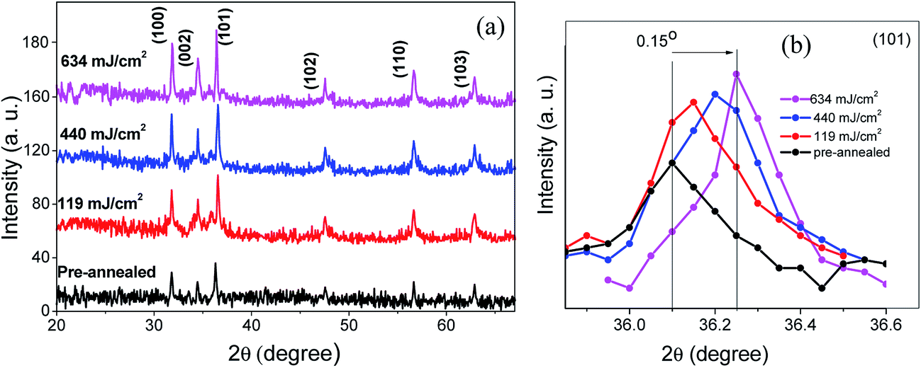 | ||
| Fig. 1 (a) X-ray diffraction patterns of ZnO:Al–Ga thin film at different laser power densities. (b) Shift in the (101) diffraction peak due to changing laser power density. | ||
Since the absorption of laser energy is controlled by the ZnO:Al–Ga thin film and the pulse repetition frequency, the crystallization of the thin films at different laser power densities is found to be varied. The absorption rate of laser energy and crystallization of ZnO:Al–Ga thin films are probably correlated with the laser repetition frequency. Thus, better crystallization occurs at higher laser power density. This improvement may be ascribed to a reduction of internal defects including inter-crystal gaps and voids or disorders in the ZnO:Al–Ga nanostructure by laser annealing.
For different laser power densities, the detected d values, lattice parameters, intensities, dislocation densities, tensile strains, grain sizes and diffraction angles (2θ) of the films are tabulated in Table 1. According to the intensity value for the two intense peaks of (100) and (101) depicted in Table 1, the higher level of crystallinity is achieved at the 634 mJ cm−2 laser power density. Moreover, the grain sizes and tensile strains of the samples are estimated by Williamson–Hall (W–H) and Scherrer plots (see equations below).29
K is a constant equal to 0.94 where βexperiment is the full width at half maximum (FWHM) of the XRD peaks; λ is the X-ray wavelength used; and θ is the Bragg's angle. The plots are not presented here, due to space constraints in this study, rather the strain and grain sizes are calculated (see Table 1). These methods are described in our recent study.30 For the ZnO–SiO2 interface, the Zn atoms are bound with two O atoms. However, the O-atoms of down sites are not able to bind with Zn atoms and instead defect sites can be created in the boundary between the SiO2 and ZnO. These defects along with the lattice incongruity among the layers produce the greatest share of compressive strain for the pre-annealed sample. The laser annealing process has a slight effect on epitaxial strain. This contributes to the lattice relaxation process through which the peaks are shifted to positions closer to those of the bulk. This can be explained with respect to changes in the interatomic distances and lattice contraction. Moreover, the dislocation density (δ) is measured by the formula below, where D is the crystallite size.31 This gives more insight into the quantity of defects in the films.
| Laser power density | hkl | 2θ ±0.01 | dhkl (nm) ±0.0002 | a, c (nm) ±0.0002 | δ ±0.0002 | ε ±0.0002 | Intensity (a.u.) | Grain size (nm) | |||
|---|---|---|---|---|---|---|---|---|---|---|---|
| Scherrer ±2 nm | W–H ±2 nm | TEM ±2 nm | FESEM ±2 nm | ||||||||
| Pre-annealed | (101) | 36.10 | 0.2485 | a = 0.3250 | 0.0065 | 0.0025 | 19 | 10 | 12 | — | 15 |
| (100) | 31.75 | 0.2856 | c = 0.5202 | 26 | |||||||
| 119 | (101) | 36.14 | 0.2482 | a = 0.3246 | 0.0027 | 0.0018 | 23 | 16 | 19 | — | 22 |
| (100) | 31.79 | 0.2852 | c = 0.5198 | 35 | |||||||
| 440 | (101) | 36.20 | 0.2478 | a = 0.3239 | 0.0010 | 0.0012 | 34 | 27 | 30 | — | 35 |
| (100) | 31.82 | 0.2846 | c = 0.5294 | 39 | |||||||
| 634 | (101) | 36.25 | 0.2475 | a = 0.3232 | 0.0011 | 0.0004 | 38 | 40 | 43 | 55 | 46 |
| (100) | 31.87 | 0.2838 | c = 0.5192 | 50 | |||||||
Therefore, a higher laser power produces a larger grain size. Thus, the β and δ values become smaller. The annealing process improves the crystallization of the films, and lowers the number of defects and dislocation density, which is clearly shown in Table 1.
The HR-TEM image of the ZnO:Al–Ga sample annealed at 634 mJ cm−2, the corresponding selected area electron diffraction (SAED) pattern and the selected focusing area are shown in Fig. 2b, c and d, respectively. To confirm the presence of Al and Ga, the EDX mapping for the sample annealed at 634 mJ cm−2 is depicted in Fig. 2e. The dopant nano-collection due to agglomeration of Al and/or Ga atoms caused by the annealing process appears in a dark color and is shown by the yellow arrows in Fig. 2a. The presence of lattice fringes obviously verifies that the material is crystalline. At the same time the crystals are placed inappropriately. The high resolution image focusing on a single particle shows the ZnO:Al–Ga lattice arrangement with a d-spacing of 1.44 Å (L1) which corresponds to the (103) plane as shown Fig. 2d. The appearance of fringes in different directions confirms the poly-orientation of the crystal. Moreover, the d-spacing of 2.4 Å (L3) is related either to pure ZnO (101), which is in good agreement with d-spacing extracted from XRD, and/or to Al2O3 (1120). The d-spacing of 3.65 Å (L2) probably originates from Ga2O3. It is supposed that Ga migrates in the presence of laser treatment, forming hexagonal Ga2O3 nanocrystals with the incorporation of oxygen present during annealing, the synthesis process or in the ZnO site.32
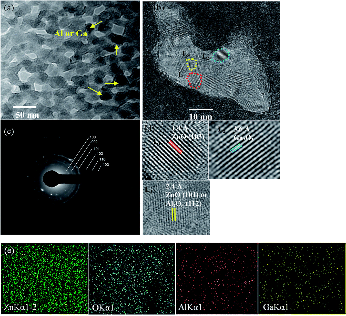 | ||
| Fig. 2 TEM images of the ZnO:Al–Ga thin film. (a) Typical TEM micrograph of sample annealed at 634 mJ cm−2 (b) HR-TEM and (c) SAED pattern of the corresponding sample. Sample exhibits a hexagonal spot pattern corresponding to the (100), (002), (101), (102), (110) and (103) planes. (d) High magnification of selected areas used to calculate d-spacings in different directions. (e) EDX mapping images of Zn, O, Al and Ga for the corresponding sample. | ||
Furthermore, the presence of Al and Ga in the ZnO lattice structure confirms the presence of a Zn–Al or Zn–Ga semiconductor nano heterostructure responsible for the visible light harvesting and suitable for optoelectronic applications. However, it was not possible to focus on the dopant position in the HR-TEM of the sample.
Fig. 3 displays the top view FESEM images of all samples. The corresponding EDX point analysis and cross section image of the pre-annealed sample are presented as an inset to part (a). The segments comprise a top layer of ZnO:Al–Ga, an intermediate layer of SiO2 and a bottom glass substrate surface. They are separated by yellow lines. The results show that the main elements presented within the inspection field include Zn, O, Al and Ga, with Zn being the most abundant element. A semi-quantitative view of the elemental composition in the inspection field in units of both weight percent and atomic percent is provided through the tabulated results.
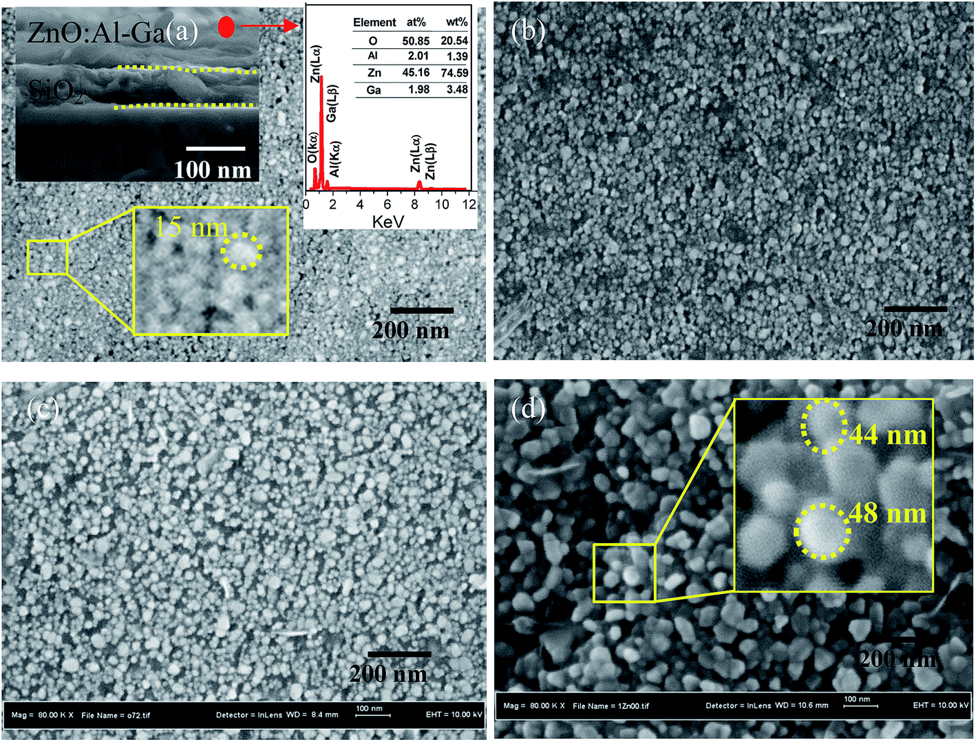 | ||
| Fig. 3 Top view FESEM images of (a) pre-annealed sample, and samples annealed at (b) 119, (c) 440 and (d) 634 mJ cm−2. The inset of figure (a) shows a high magnification of the selected area cross section FESEM to confirm the formation of layers and the point EDX. The inset of figure (d) shows a high magnification of the selected area. | ||
Both the macroscale temperature evolution history of the ZnO:Al–Ga film and the nanoscale atomic motion/mass transport of the ZnO:Al–Ga nanoparticle stack during laser annealing suggest that, through laser treatment, the closely packed ZnO:Al–Ga nanoparticle film sustains three processes. Initially, the ZnO:Al–Ga nanoparticle stack appears to be cubic close packed (ccp) right after coating (Fig. 3a). During annealing, the hot spots formed over contacts tend to drive the surface melting and merging together of small particles. This process tends to enlarge the grain size, modify the grain shape and compact internal gaps (Fig. 3b and c). Finally by further increasing the laser power, a much denser film stack is formed, where faceted large grains are achieved and impinge on each other (Fig. 3d).
Comparing the samples in-process to the finally treated area (Fig. 3d), it is found that the crystallized film is more compact and continuous, suggesting that the crystallinity of the ZnO:Al–Ga film has been considerably enhanced. The good film homogeneity and crystallinity result from grain growth, shape change and the removal of inter-grain defects like voids, gaps and discontinuities.
Fig. 4(a) shows the optical transmittance spectra of the ZnO:Al–Ga films. In all samples, acceptable optical transmittance and small reflectance in the visible wavelength area are found. The oscillations in the visible region are shown by transmittance and reflectance. The constructive and destructive interference among multiple bounce beams are responsible for these oscillations in the spectra. A sharp edge exists between 350 nm and 400 nm which is due to the inter-band absorption edge. The average optical transmittance in the visible range goes above 85% for samples annealed at 440 and 634 mJ cm−2. A sharp absorption cut-off is obviously seen. The equation below clearly demonstrates the dependence of absorption index (α) on illumination wavelength (see Fig. 4(b)):
| αhν ∝ (hν − Eg)1/2 |
where ΔEBM is the blue-shift of the optical band; h is Planck's constant; n is the carrier concentration; and m* is the electron effective mass in the conduction band.34 Hence, the increment in carrier concentration contributes to the increment in Eg. The Eg values of the samples are decreased sharply by increasing the laser power up to 634 mJ cm−2. This is ascribed to the larger grain size, the consequence of electrostatic potentials and a decrease in the carrier concentration (shown later in Fig. 8b).35
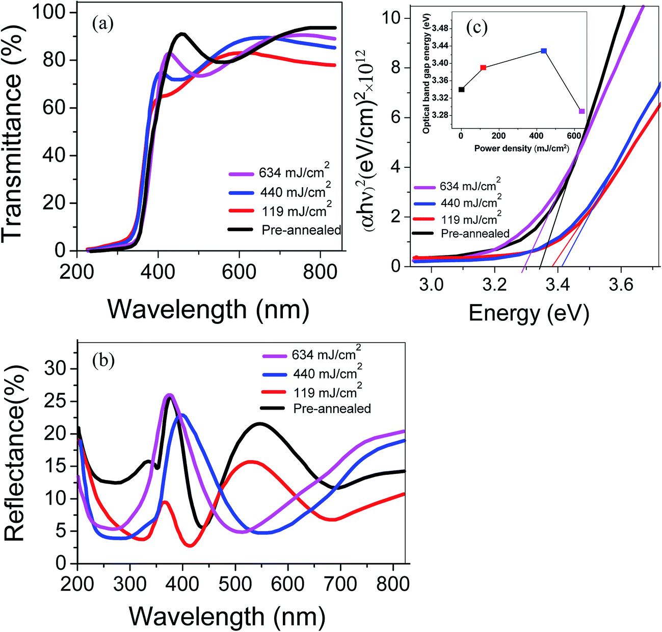 | ||
| Fig. 4 (a) Transparency and (b) reflectance spectra of ZnO:Al–Ga at different laser power densities, and (c) optical band gap of ZnO:Al–Ga films. | ||
The refractive index n and extinction coefficient k of the samples derived from model-fitting the experimental spectroscopic ellipsometric data are shown in Fig. 5. As can be seen from the figure, both n and k first decrease and then increase with the laser power density. This might be largely ascribed to the increment in the carrier concentration in the ZnO:Al–Ga films. The increase of n and k should be correlated to an increment in the density of the film as it is compacted.21 The essential electron excitation spectra of the films are labeled by the frequency dependence of the complex dielectric constant. The real and imaginary parts of the dielectric constant are determined in the following equations:
| εreal = n2 − k2 |
| εimaginary = 2nk |
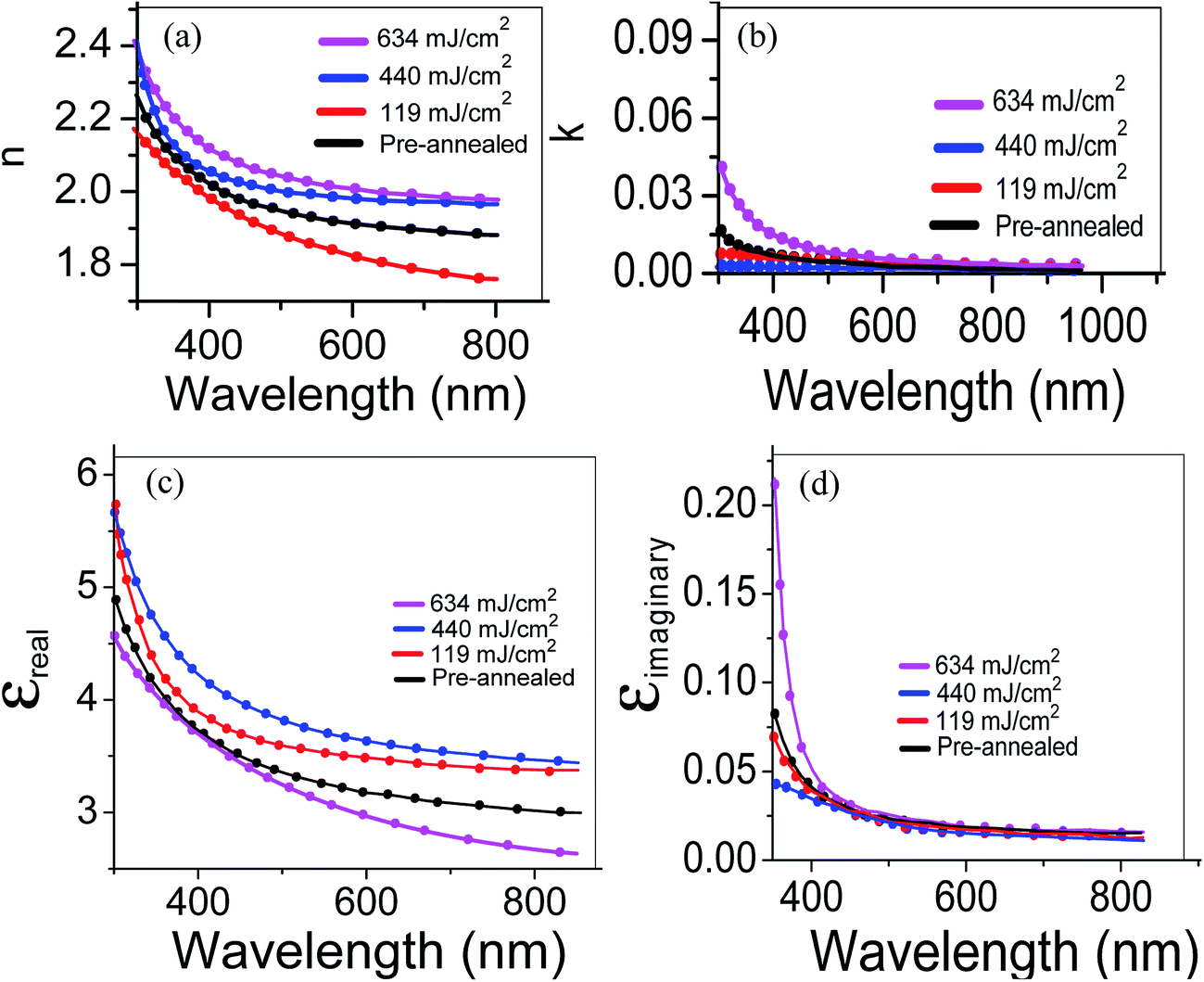 | ||
| Fig. 5 Variations in (a) refractive index, (b) extinction coefficient, and (c) real and (d) imaginary parts of the dielectric constants of ZnO:Al–Ga thin films. | ||
The real and imaginary parts of the dielectric constant (εreal and εimaginary) are depicted in Fig. 5c and d respectively. From Fig. 5, it is observed that εreal and εimaginary values reduce with wavelength. It is assumed that the dielectric constants of the films can be associated to the extinction coefficients and refractive indexes.
It is clear that vibrational properties of solids are related to the long and short-range orders in the spatial array of the constituent atoms. Raman spectroscopy is implemented on the pre-annealed and annealed samples in order to examine the influence of laser annealing power on the vibrational properties of the ZnO:Al–Ga nanostructures. The symmetry of wurtzite ZnO lies in the spatial group c6v4, having two formula units in the primitive cell. Thus, the optical phonons at the center of the Brillouin zone (G) are described by the following irreducible relation:36
| Γ = 1A1 + 2B1 + 1E1 + 2E2 |
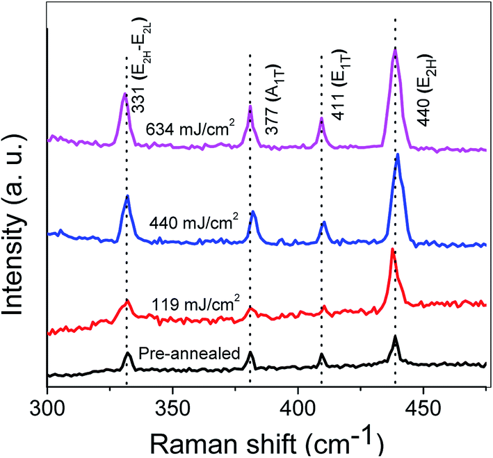 | ||
| Fig. 6 Raman spectra of samples at different power densities. | ||
The peaks centered at about 331 cm−1 have been previously examined in ZnO by other researchers38–41 to describe the second order modes or multi-phonon processes.
The enhancement of the LO phonon mode with increasing laser power might occur because of the intra-band Frohlich interaction. Group III–V semiconductors are generally considered under (or close to) resonant conditions, where LO-phonon scattering is dipole-forbidden. The mode is strongly improved in nanostructures such as nanoparticles because of (partial) splitting of the electron and hole clouds (created by the incident laser photon) in the space.42 Moreover, LO phonons participating in the scattering are expected to be a mixture of A1 and E1 modes due to the symmetry breaking caused by the laser annealing. Thus, the slight increase of peak intensity by laser annealing can be explained. Furthermore, the enhancement in the intensity of Raman peaks may also be attributed to the modified crystallinity of the nanostructures because of the annealing process, as can be seen from the XRD patterns.
Fig. 7 illustrates the room-temperature PL spectra of the pre-annealed ZnO:Al–Ga thin film and the films annealed at various temperatures. The spectra can be divided into UV (∼370 nm) and visible light (450–650 nm) parts (see Fig. 7). The UV emission associated with free exciton–exciton collision processes is ascribed to the near band edge (NBE). The visible emission of ZnO thin films happens because of defects which form deep energy levels in the band gap. A schematic diagram of the energy levels of defects, e.g. oxide vacancy (VO), oxide antisite defect (OZn), interstitial oxygen (Oi), interstitial zinc (Zni) and zinc vacancy (VZn) in ZnO thin films is shown in Fig. 7.43
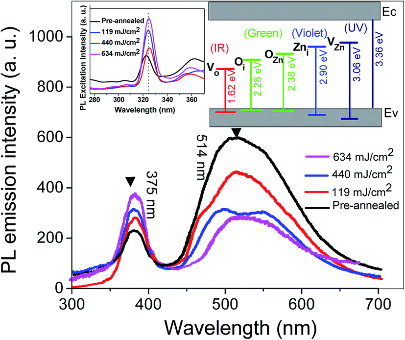 | ||
| Fig. 7 Room temperature PL spectra of samples annealed at different laser power densities. The inset indicates the schematic band diagram based on PL data. | ||
The spectra of ZnO:Al–Ga thin films in the pre-annealed state and when annealed at 119 mJ cm−2 involve a weak UV emission at ∼375 nm as well as a strong broad green emission at ∼514 nm (2.40 eV). When the films are annealed at 440 or 634 mJ cm−2, the peak intensity at 375 nm is gradually increased which is ascribed to the greater amount of photo-carrier recombination in the NBE due to the increasing laser power density. When the annealing power is increased to 634 mJ cm−2, interstitial oxygen (Oi) defects become unstable and the amount of interstitial oxygen (Oi) diffusing into the oxygen vacancies (VO) and oxygen interstitial (Oi) defects further decreases. This results in a reduction in the green emission intensity. The decrease in green emission happens because of decreasing nonradiative defects and increasing grain size.44
Fig. 8 displays the room temperature dependence of resistivity, carrier concentration and mobility as a function of power density calculated by Hall measurement. Changing the laser power density has a measurable effect on the electrical properties of the films. It is well-known that the resistivity is proportional to the reciprocal of the product of carrier concentration and mobility. For power densities lower than 440 mJ cm−2, the resistivity of the ZnO:Al–Ga film is decreased by power density, which is attributed to the increment in carrier concentration made by the laser-activated Al and Ga ions and decrement of oxygen vacancies.45 By increasing the power density to 634 mJ cm−2, the resistivity of the ZnO:Al–Ga films increases, which is largely due to the decrement of mobility shown in Fig. 8c. The mobility of thin films with carrier concentrations of ∼1.7 to 2.2 × 1019 cm−3 is defined using both ionized impurity scattering and grain boundary scattering. The decrement of mobility is ascribed to the scattering which happens due to the grain boundary shown in the FESEM images in Fig. 3.
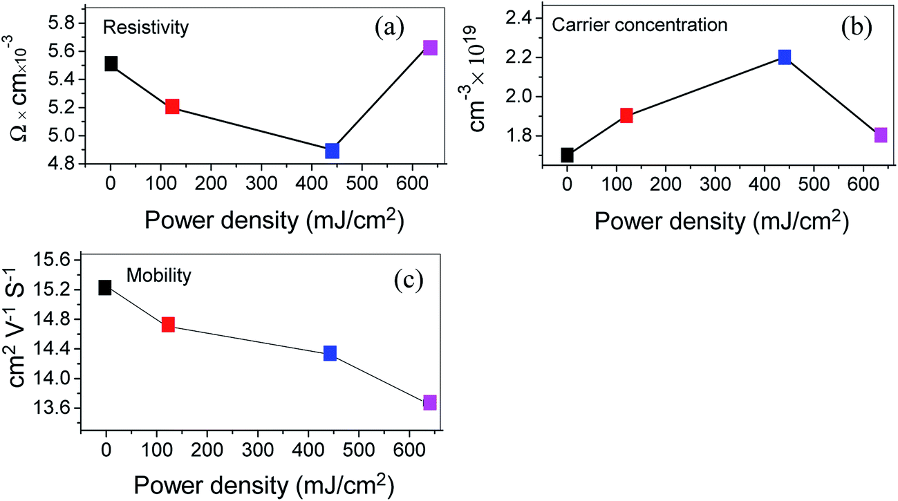 | ||
| Fig. 8 Electrical properties of ZnO:Al–Ga thin films as a function of laser power density. | ||
Fig. 9 illustrates the wide scan X-ray photoelectron spectra (XPS) and their Gaussian-resolved components of Al 2p3/2, O 1s, Zn 2p3/2, Zn 2p1/2 and Ga 2p3/2 for the 634 mJ cm−2 power density sample. The XPS spectra reveal valuable information about elemental compositions and bonding states for each constituent element of the deposited films. A wide scan spectrum of the film confirms the appearance of Zn 2p, Zn 3s, Zn 3p, Zn 3d, O 1s and Auger lines. The bonding energy correlated with the different components of O 1s, Zn 2p3/2, Zn 2p1/2, Al 2p3/2 and Ga 2p3/2, are shown in Fig. 9b, c, d, e and f respectively.46,47 The symmetrical signal of Zn 2p which is depicted in Fig. 9c and d correlates to the covalent structure of ZnO. No apparent peak shifting or intensity variation can be observed as a result of the annealing process. The asymmetric Auger signal at an energy of ∼586 eV is ascribed to the bonding of Zn with oxygen in the ZnO lattice. A shoulder peak at ∼574 eV corresponds to the existence of Zn interstitials in the films that are one of the major sources of free electrons in doped ZnO films.48 Similarly, there is no annealing power effect on the intensity of Auger signals. The green Gaussian fit in the O 1s peak is usually attributed to chemisorbed or dissociated oxygen or OH species on the film surface.44 It is well known that oxygen vacancies can create free electrons, while chemisorbed oxygen or OH species can capture free electrons which are responsible for the existence of carriers.
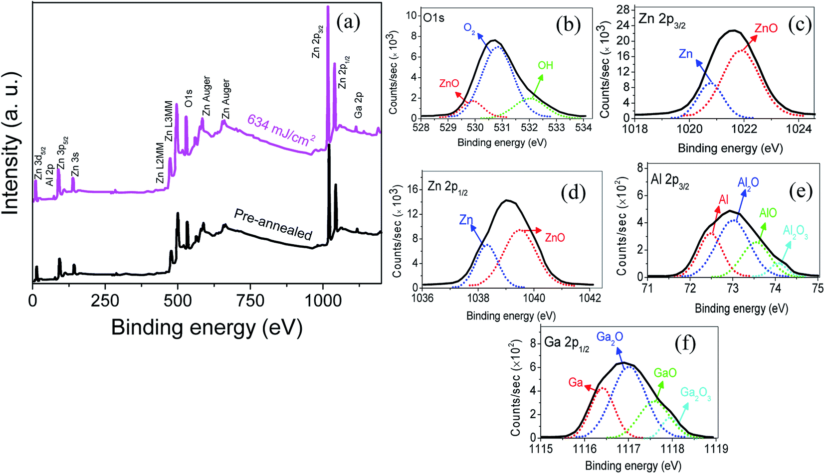 | ||
| Fig. 9 XPS spectra for the sample annealed at a power density of 634 mJ cm−2. (a) Overall XPS spectra of the pre-annealed and annealed samples, and the Gaussian-resolved components of (b) O 1s, (c) Zn 2p3/2, (d) Zn 2p1/2, (e) Al 2p3/2, and (f) Ga 2p1/2. | ||
4. Conclusion
The effect of laser annealing at different power densities on the structural, optical and electrical properties of ZnO:Al–Ga/SiO2/glass synthesized by rf magnetron sputtering, sol–gel and spin coating has been studied systematically. While a combination of Al and Ga dopants encourages lattice defects in the ZnO nanostructures, laser annealing improves the crystalline quality due to a reduction in the number of internal defects, including inter-crystal gaps, voids and disorders. The carrier concentration, mobility and resistivity of ZnO:Al–Ga films vary considerably as the laser power density is increased. The transmittances of the ZnO:Al–Ga films remain at around 85% in the visible region. Additionally, the absorption cut-off wavelength of ZnO:Al–Ga films annealed at a lower power density shift to shorter wavelength due to the BM effect. However, after higher power density annealing of ZnO:Al–Ga films, red-shifts are found in the absorption cut-off wavelength. This could be ascribed to the smaller grain boundary and larger grain size. The present study examines the films through Raman spectroscopy to show the way in which laser annealing results in the manifestation of an intense and broad band in the spectral region close to the LO phonon frequencies due to the intra-band Frohlich interaction and the improvement in crystallinity. The photoluminescence results indicate that the laser power density can tune the luminescence efficiency of the samples. Both the refractive indexes and the extinction coefficients of the samples first decrease and then increase with the laser power density. This behavior can be explained by the change in the carrier concentration and film compaction.Acknowledgements
The project was supported by the Universiti Teknologi Malaysia, AMTEC through Research Grant Vote number R.J130000.7609.4C112, and the Frontier material research alliance.References
- D. C. Look, Recent advances in ZnO materials and devices, Mater. Sci. Eng., B, 2001, 80(1), 383–387 CrossRef.
- Q.-X. Yu, B. Xu, Q.-H. Wu, Y. Liao, G.-Z. Wang and R.-C. Fang, et al., Optical properties of ZnO/GaN heterostructure and its near-ultraviolet light-emitting diode, Appl. Phys. Lett., 2003, 83(23), 4713–4715 CrossRef CAS.
- D. Bagnall, Y. Chen, Z. Zhu, T. Yao, S. Koyama and M. Y. Shen, et al., Optically pumped lasing of ZnO at room temperature, Appl. Phys. Lett., 1997, 70(17), 2230–2232 CrossRef CAS.
- D. Zhang, T. Yang, J. Ma, Q. Wang, R. Gao and H. Ma, Preparation of transparent conducting ZnO: Al films on polymer substrates by rf magnetron sputtering, Appl. Surf. Sci., 2000, 158(1), 43–48 CrossRef CAS.
- Q. Ahsanulhaq, J. H. Kim, J. H. Kim and Y. Hahn, Seedless pattern growth of quasi-aligned ZnO nanorod arrays on cover glass substrates in solution, Nanoscale Res. Lett., 2010, 5(3), 669 CrossRef CAS PubMed.
- Y. Lee, H. Kim and Y. Roh, Deposition of ZnO thin films by the ultrasonic spray pyrolysis technique, Jpn. J. Appl. Phys., 2001, 40(4R), 2423 CrossRef CAS.
- M. Berber, V. Bulto, R. Kliß and H. Hahn, Transparent nanocrystalline ZnO films prepared by spin coating, Scr. Mater., 2005, 53(5), 547–551 CrossRef CAS.
- J.-L. Deschanvres, B. Bochu and J.-C. Joubert, Deposition conditions for the growth of textured ZnO thin films by aerosol CVD process, J. Phys. IV, 1993, 3(C3), C3485–C3491 CrossRef.
- M. Liu, X. Wei, Z. Zhang, G. Sun, C. Chen and C. Xue, et al., Effect of temperature on pulsed laser deposition of ZnO films, Appl. Surf. Sci., 2006, 252(12), 4321–4326 CrossRef CAS.
- I. Sayago, M. Aleixandre, L. Ares, M. Fernandez, J. Santos and J. Gutierrez, et al., The effect of the oxygen concentration and the rf power on the zinc oxide films properties deposited by magnetron sputtering, Appl. Surf. Sci., 2005, 245(1), 273–280 CrossRef CAS.
- Growth mechanism of chemically prepared ZnO–SiO2 nanostructures grown on glass and silicon substrates, IOP Conference Series: Materials Science and Engineering, ed. K. Simfroso, R. Candidato Jr, F. Bagsican, M. Jabian, M. Odarve, G. Paylaga, et al., IOP Publishing, 2015 Search PubMed.
- J. Lv and Y. Liu, Spectroscopic evidence that Li doping creates shallow V Zn in ZnO, Phys. Chem. Chem. Phys., 2017, 19(8), 5806–5812 RSC.
- S. B. Ameur, A. Barhoumi, R. Mimouni, M. Amlouk and H. Guermazi, Low-temperature growth and physical investigations of undoped and (In, Co) doped ZnO thin films sprayed on PEI flexible substrate, Superlattices Microstruct., 2015, 84, 99–112 CrossRef.
- D.-K. Kim and H.-B. Kim, Substrate temperature effects on the electrical properties of sputtered Al doped ZnO thin films, Superlattices Microstruct., 2015, 85, 50–58 CrossRef CAS.
- A. Ali, X. Zhao, A. Ali, L. Duan, H. Niu and C. Peng, et al., Enhanced photocatalytic activity of ZnO nanorods grown on Ga doped seed layer, Superlattices Microstruct., 2015, 83, 422–430 CrossRef CAS.
- A. Janotti and C. G. Van de Walle, Fundamentals of zinc oxide as a semiconductor, Rep. Prog. Phys., 2009, 72(12), 126501 CrossRef.
- W. Lee, S. Shin, D.-R. Jung, J. Kim, C. Nahm and T. Moon, et al., Investigation of electronic and optical properties in Al–Ga codoped ZnO thin films, Curr. Appl. Phys., 2012, 12(3), 628–631 CrossRef.
- J. Lu, L. Zhu, Z. Ye, F. Zhuge, Y. Zeng and B. Zhao, et al., Dependence of properties of N–Al codoped p-type ZnO thin films on growth temperature, Appl. Surf. Sci., 2005, 245(1), 109–113 CrossRef CAS.
- J. C. Fan, K. Sreekanth, Z. Xie, S. Chang and K. V. Rao, p-Type ZnO materials: theory, growth, properties and devices, Prog. Mater. Sci., 2013, 58(6), 874–985 CrossRef CAS.
- A. J. Gross and T. R. Herrmann, History of lasers, World J. Urol., 2007, 25(3), 217–220 CrossRef PubMed.
- M. Bertolotti, A. Ferrari, A. Jaskow, A. Palma and E. Verona, Laser annealing of ZnO thin films, J. Appl. Phys., 1984, 56(10), 2943–2947 CrossRef CAS.
- K. Kim, S. Kim and S. Y. Lee, Effect of excimer laser annealing on the properties of ZnO thin film prepared by sol–gel method, Curr. Appl. Phys., 2012, 12(2), 585–588 CrossRef.
- T. Nagase, T. Ooie, Y. Makita, S. Kasaishi, M. Nakatsuka and N. Mizutani, Morphology, Structure and Photoluminescence Properties of Zinc Oxide Films Prepared by Excimer Laser Irradiation of Sol–Gel-Derived Precursors, Jpn. J. Appl. Phys., 2001, 40(11R), 6296 CrossRef CAS.
- T. Nagase, T. Ooie and J. Sakakibara, A novel approach to prepare zinc oxide films: excimer laser irradiation of sol–gel derived precursor films, Thin Solid Films, 1999, 357(2), 151–158 CrossRef CAS.
- W. M. Tsang, F. L. Wong, M. K. Fung, J. Chang, C. S. Lee and S. T. Lee, Transparent conducting aluminum-doped zinc oxide thin film prepared by sol–gel process followed by laser irradiation treatment, Thin Solid Films, 2008, 517(2), 891–895 CrossRef CAS.
- A. Samavati, H. Nur, A. F. Ismail and Z. Othaman, Radio frequency magnetron sputtered ZnO/SiO2/glass thin film: Role of ZnO thickness on structural and optical properties, J. Alloys Compd., 2016, 671, 170–176 CrossRef CAS.
- G. M. Nam and M. S. Kwon, Transparent conducting Ga-doped ZnO thin film for flat-panel displays with a sol–gel spin coating, J. Inf. Disp., 2008, 9(3), 8–11 CrossRef.
- B. D. Ahn, H. S. Kang, J. H. Kim, G. H. Kim, H. W. Chang and S. Y. Lee, Synthesis and analysis of Ag-doped ZnO, J. Appl. Phys., 2006, 100(9), 093701 CrossRef.
- B. D. Cullity and J. W. Weymouth, Elements of X-ray Diffraction, Am. J. Phys., 1957, 25(6), 394–395 CrossRef.
- A. Samavati, Z. Othaman, S. Ghoshal and M. Mustafa, The influence of growth temperature on structural and optical properties of sputtered ZnO QDs embedded in SiO2 matrix, Superlattices Microstruct., 2015, 86, 134–142 CrossRef CAS.
- W. D. Callister Jr and D. G. Rethwisch, Fundamentals of materials science and engineering: an integrated approach, John Wiley & Sons, 2012 Search PubMed.
- R. Jalilian, M. Yazdanpanah, B. Pradhan and G. Sumanasekera, Crystalline nano-structures of Ga2O3 with herringbone morphology, Chem. Phys. Lett., 2006, 426(4), 393–397 CrossRef CAS.
- V. Srikant and D. Clarke, Optical absorption edge of ZnO thin films: the effect of substrate, J. Appl. Phys., 1997, 81(9), 6357–6364 CrossRef CAS.
- C. E. Kim, P. Moon, S. Kim, J.-M. Myoung, H. W. Jang and J. Bang, et al., Effect of carrier concentration on optical bandgap shift in ZnO: Ga thin films, Thin Solid Films, 2010, 518(22), 6304–6307 CrossRef CAS.
- J.-P. Lin and J.-M. Wu, The effect of annealing processes on electronic properties of sol–gel derived Al-doped ZnO films, Appl. Phys. Lett., 2008, 92(13), 134103 CrossRef.
- C. Arguello and D. Rousseau, Porto SPdS. First-order Raman effect in wurtzite-type crystals, Phys. Rev., 1969, 181(3), 1351 CrossRef CAS.
- C. Xu, X. Sun, X. Zhang, L. Ke and S. Chua, Photoluminescent properties of copper-doped zinc oxide nanowires, Nanotechnology, 2004, 15(7), 856 CrossRef CAS.
- T.-L. Phan, R. Vincent, D. Cherns, N. H. Dan and S.-C. Yu, Enhancement of multiple-phonon resonant Raman scattering in co-doped ZnO nanorods, Appl. Phys. Lett., 2008, 93(8), 082110 CrossRef.
- J. Ye, S. Gu, S. Zhu, S. Liu, Y. Zheng and R. Zhang, et al., Raman study of lattice dynamic behaviors in phosphorus-doped ZnO films, Appl. Phys. Lett., 2006, 88(10), 101905 CrossRef.
- Z. Cheng, X. Wang, S. Dou, K. Ozawa, H. Kimura and P. Munroe, Fabrication, Raman spectra and ferromagnetic properties of the transition metal doped ZnO nanocrystals, J. Phys. D: Appl. Phys., 2007, 40(21), 6518 CrossRef CAS.
- M. Jang, M. Ryu, M. Yoon, S. Lee, H. Kim and A. Onodera, et al., A study on the Raman spectra of Al-doped and Ga-doped ZnO ceramics, Curr. Appl. Phys., 2009, 9(3), 651–657 CrossRef.
- A. Rolo and M. Vasilevskiy, Raman spectroscopy of optical phonons confined in semiconductor quantum dots and nanocrystals, J. Raman Spectrosc., 2007, 38(6), 618–633 CrossRef CAS.
- A. B. Djurišić and Y. H. Leung, Optical properties of ZnO nanostructures, Small, 2006, 2(8–9), 944–961 CrossRef PubMed.
- S.-H. Jeong, J.-K. Kim and B.-T. Lee, Effects of growth conditions on the emission properties of ZnO films prepared on Si (100) by rf magnetron sputtering, J. Phys. D: Appl. Phys., 2003, 36(16), 2017 CrossRef CAS.
- W. Wang, C. Li, J. Zhang and X. Diao, Effects of atomic oxygen treatment on structures, morphologies and electrical properties of ZnO: Al films, Appl. Surf. Sci., 2010, 256(14), 4527–4532 CrossRef CAS.
- K. Uma, M. Rusop, T. Soga and T. Jimbo, Effects of Al content on Zn0. 95Mg0. 05O thin films deposited by sol–gel spin coating, Jpn. J. Appl. Phys., 2007, 46(1R), 40 CrossRef CAS.
- M. Chen, X. Wang, Y. Yu, Z. Pei, X. Bai and C. Sun, et al., X-ray photoelectron spectroscopy and auger electron spectroscopy studies of Al-doped ZnO films, Appl. Surf. Sci., 2000, 158(1), 134–140 CrossRef CAS.
- F.-H. Wang, Y.-H. Lee, T.-K. Kang and H.-W. Liu, Influence of RF power on physical properties of ZnO: ZnF2 thin films by RF magnetron sputtering, Superlattices Microstruct., 2015, 83, 289–298 CrossRef CAS.
| This journal is © The Royal Society of Chemistry 2017 |