
 Open Access Article
 This Open Access Article is licensed under a Creative Commons Attribution-Non Commercial 3.0 Unported Licence
Improved sensitivity of UV sensors in hierarchically structured arrays of network-loaded ZnO nanorods via optimization techniques†
Seyed Farshad Akhtarianfar ad,
Ali Khayatianb,
Rouhollah Shakernejadb,
Mohammad Almasi-Kashi*ab and
Suck Won Hong*c
ad,
Ali Khayatianb,
Rouhollah Shakernejadb,
Mohammad Almasi-Kashi*ab and
Suck Won Hong*c
aInstitute of Nanoscience and Nanotechnology, University of Kashan, Kashan 87317-51167, Iran. E-mail: almac@kashanu.ac.ir
bDepartment of Physics, University of Kashan, Kashan 87317-51167, Iran
cDepartment of Cogno-Mechatronics Engineering, Department of Optics and Mechatronics Engineering, Pusan National University (PNU), Busan 46241, Republic of Korea. E-mail: swhong@pusan.ac.kr
dOptomechatronics Research Institute, Pusan National University (PNU), Busan 46241, Republic of Korea
First published on 23rd June 2017
Abstract
Hierarchical nanostructures have received much attention in recent years for their enhanced fundamental properties and potential applications in manifold areas. Herein, we report a simple and robust strategy for the fabrication of hierarchically nanostructured arrays of network-loaded ZnO nanorods (NRs) for use in UV photodetectors based on comprehensively optimized experimental conditions using the Taguchi approach. Specifically, the critical roles of the morphological and structural characteristics of ZnO NRs on the UV sensing properties are systematically evaluated. Results show that the specific deposition conditions of the secondary colloidal ZnO NRs onto the surface of the vertically grown ZnO NRs contribute to the formation of tightly organized networks over large areas, which act as favorable energy junction barriers, and thus play a significant role in enhancing the performance of the UV photodetector. Under optimal conditions, the sensitivity of the prepared UV sensors was improved to 8000, which has not been reported yet in the field of ZnO-based UV sensors with vertical networked nanostructures. Our comprehensive studies to optimize sensitivity, responsivity, and response/recovery times suggest a highly viable route for practical applications in photodetectors using this facile implementation of ZnO NRs.
1. Introduction
Ultraviolet (UV) photodetectors have great potential in a wide range of applications such as chemical and biological analysis, environmental monitoring, flame and radiation detection, space communication, and military areas.1–4 To develop these applications, nanoscale semiconducting materials have been extensively used as building blocks for better-performance UV photodetectors with high sensitivities and rapid responses.5 Compared to their thin-film or bulk forms, nanostructured materials, particularly one-dimensional types such as nanorods or nanowires, have exhibited excellent response, selectivity, and sensitivity properties because of their high surface-to-volume ratios and unique physicochemical properties.6,7 To date, extensive work has been carried out on wide-band gap materials for UV sensing applications, such as ZnO, Ga2O3, SnO2, ZnS, SiC, and GaN.8–13 ZnO nanostructures have been widely used as intrinsic n-type semiconducting elements in field-effect transistors,14 chemical sensors,15 piezoelectric nanogenerators,16 and photodetectors17 because of their outstanding optoelectronic, mechanical, and structural properties, including direct wide bandgap (3.37 eV) and large exciton binding energy (∼60 meV),18 Moreover, recent studies have led to many advances in techniques for synthesizing one-dimensional ZnO nanostructures (i.e., nanorods, nanobelts, or nanowires).19 Among these methods, the hydrothermal method is the most attractive technique, as it offers a means of obtaining well-ordered ZnO nanostructures without the need for lithography (or other external fields) over large surface areas on various types of substrates using a low-cost facile route.20,21 Thus far, to enhance the performance of UV photodetectors, various designs and geometrical parameters for the hydrothermal growth process have been investigated for use in the fabrication of ZnO nanostructures.22,23In this study, we present a simple and straightforward method for fabricating a UV photodetector, consisting of hierarchically organized arrays of network-loaded ZnO nanorods (NRs) over very large coverage areas by combining two consecutive processes. The main strategy involves optimized direct growth of ZnO NRs on a substrate and a careful deposition process for separately prepared colloidal ZnO NRs, because the spatial network loading of ZnO NRs occurs in a subsequent step. First, the controlled hydrothermal growth procedure for ZnO NRs was applied via the repeated addition of fresh precursor solution to compensate for the depletion of the reagents used to maintain the temperature and pH, in addition to the formation of a highly uniform dip-casted seed layer (Fig. 1a, see the Experimental section for details). Subsequently, a programmed dip-coating process was applied to the colloidal ZnO NRs to produce network-like nanostructures on the firstly grown vertically oriented ZnO surface (Fig. 1b). Using this bottom-up approach, vertical nanoscopic bridged network-bundles of self-organized ZnO NRs form due to an increase in the alignment forces, with comparable one-dimensional geometric environments that span the entire substrate. This approach is effective for the direct integration of network-loaded nanostructures on top of a firstly grown ZnO NR substrate, but after some point, the dip-coating tends to yield bundles of ZnO NRs and limits the density control over the entire substrate. This behavior results from the near-surface interaction mode between the ZnO NRs observed in these systems, in which even very slight relief at the tip of the firstly provided vertically grown ZnO NRs surface, associated with either the tight interface of ZnO NRs or with van der Waals forces between the colloidal ZnO NRs, can induce a different structural mode. A different strategy that also involves optimized density (i.e., the number of networks) relies on possible combinations and permutations of many effective control-parameters (i.e., concentration, deposition cycles, and deposition time). Therefore, fabrication and optimization of networked ZnO NR nanostructures with the minimum number of experiments can be determined using optimized control of multiple effective parameters. Thus, the factorial design of experiments (i.e., the Taguchi method) is used to fully exploit our strategy,24 which has recently been developed in process monitoring in the field of nanofabrication.25,26 The basic principle of this technique is investigation of the effects of experimental variables on the synthetic procedure using orthogonal arrays to design the minimum number of necessary experiments. Taguchi design of an experiment model refers to the study of any given system based on a set of independent parameters (i.e., factors) over a particular region of interest (i.e., levels).27
 | ||
| Fig. 1 Stepwise representation of the fabrication of UV detection device based on double-layered structured ZnO NRs. (a) Hydrothermally grown ZnO NRs on the dip-coated catalytic seed layer (bottom left: top-view SEM and AFM images of the uniformly coated seed layer and bottom right: SEM images of each top and cross-section view of vertically grown ZnO NRs with the average diameter of ∼80 nm and length of ∼1.7 μm). (b) Controlled dip-coating of colloidal ZnO NRs on the first grown ZnO NRs; scooping process from the well-dispersed ZnO colloidal solution with angle θ of 30° and the schematic illustration of double-layer structured ZnO NRs on a glass substrate (right inset: SEM image of surface of second layer of ZnO NRs with as-grown ZnO NRs after the deposition). (c) Digital image of the fabricated UV sensor (left) and the schematic illustration of the formation of Au-deposited pads for electrical contacts (right). | ||
In the present study, we design the fabrication of vertically network-bridged ZnO NR arrays based on comprehensive optimization, that is highly reproducible, via the minimum number of necessary experiments. Results showed that the junctions between the network-loaded ZnO nanostructure arrays significantly improved the UV sensing characteristics of the photodetectors. In the optimal condition, the sensor sensitivity was improved to approximately 8000. Our proposed technique enables networked-loaded nanostructures of ZnO NRs to be optimized in terms of sensitivity, responsivity, response, and recovery time of the UV photodetector, which may be highly favorable in practical applications.
2. Experimental
2.1. Preparation of ZnO NRs arrays and network-loaded ZnO NRs
Vertically aligned ZnO NR arrays were fabricated on a uniformly dip-coated seed layer on a glass substrate, as previously reported.28 The seed layer precursor contained zinc acetate dihydrate [Zn(CH3COO)2·2H2O, reagent grade, Merck] and diethanolamine (C4H11NO2, 99% reagent grade, Merck) dissolved in ethanol (C2H5OH, 99.9%, reagent grade, Merck). For all solutions, the zinc acetate concentration was set to 0.45 M, whereas the ratio of diethanolamine to zinc acetate dihydrate was constant (i.e., 6![[thin space (1/6-em)]](https://www.rsc.org/images/entities/char_2009.gif) :5). Next, the colloidal suspensions of ZnO NRs were hydrothermally synthesized in an aqueous solution of 0.001 M zinc nitrate [Zn(NO3)2·6H2O, 98%, Acros Organics] and 0.1 M sodium hydroxide at 70 °C for 90 min using ZnO nanoparticles (average diameter of approximately 30 nm), acting as floating seeds for the nucleation of the nanorods. Then, the obtained precipitates were washed several times with deionized water (DI) and centrifuged with water and ethanol. After drying, the powder-type ZnO NRs were heat-treated in air at 300 °C for 1 h. To prepare the ZnO NR networks over vertically aligned NR arrays, the colloidal ZnO NRs were dispersed using ultrasonication for 240 s in DI water with different concentrations of 0.5, 1.0, and 1.5 mg ml−1. To prevent the temperature from increasing during ultrasonication, the homogenizing pulse mode was used for 4 s and 7 s for ON and OFF times, respectively (Fig. S1†). After the preparation of the ZnO NR colloidal suspension, vertically aligned ZnO NRs grown on a 0.5 cm × 0.5 cm silica glass substrate were dipped into the ZnO NR solution (c = 0.5, 1.0, or 1.5 mg mL−1) using a custom-made dip-coating system at a constant speed of 4 cm min−1, stopped for 60, 180, or 300 s (called the deposition time), and then, were removed from the suspension. The deposition number (times for each sample) was 1, 3, and 5. The samples were then cleaned with DI water to remove the residual salts and annealed at 300 °C for 1 h.
:5). Next, the colloidal suspensions of ZnO NRs were hydrothermally synthesized in an aqueous solution of 0.001 M zinc nitrate [Zn(NO3)2·6H2O, 98%, Acros Organics] and 0.1 M sodium hydroxide at 70 °C for 90 min using ZnO nanoparticles (average diameter of approximately 30 nm), acting as floating seeds for the nucleation of the nanorods. Then, the obtained precipitates were washed several times with deionized water (DI) and centrifuged with water and ethanol. After drying, the powder-type ZnO NRs were heat-treated in air at 300 °C for 1 h. To prepare the ZnO NR networks over vertically aligned NR arrays, the colloidal ZnO NRs were dispersed using ultrasonication for 240 s in DI water with different concentrations of 0.5, 1.0, and 1.5 mg ml−1. To prevent the temperature from increasing during ultrasonication, the homogenizing pulse mode was used for 4 s and 7 s for ON and OFF times, respectively (Fig. S1†). After the preparation of the ZnO NR colloidal suspension, vertically aligned ZnO NRs grown on a 0.5 cm × 0.5 cm silica glass substrate were dipped into the ZnO NR solution (c = 0.5, 1.0, or 1.5 mg mL−1) using a custom-made dip-coating system at a constant speed of 4 cm min−1, stopped for 60, 180, or 300 s (called the deposition time), and then, were removed from the suspension. The deposition number (times for each sample) was 1, 3, and 5. The samples were then cleaned with DI water to remove the residual salts and annealed at 300 °C for 1 h.
2.2. Design of experiments using the Taguchi method
The Taguchi method was used to obtain an efficient nanonetwork-loaded ZnO NR array UV sensor based on the optimization of the effective control parameters. Notably, instead of testing all of the possible experiment combinations, this technique tests pairs of combinations, which helps to determine the main experimental factors (i.e., concentration, deposition cycles, and deposition time). This approach significantly influences the properties of ZnO photodetectors (i.e., sensitivity, responsivity, response time, and recovery time) based on guidance from the minimum number of experiments. The selection of orthogonal arrays is based on the number of parameters and the levels of variation for each factor. The results from the orthogonal arrays can be analyzed by plotting the data and performing analysis of variance (ANOVA) to test the accuracy of the results. The accuracy of the fitted model is important to avoid misleading conclusions under a specified model system. Thus, each data point has residual values that is defined as differences between the observed values (i.e., the experimental results) and the predicted values (i.e., predicted modelling). As shown in Fig. S3,† the collective sets of graphs display the responses of residual values versus observation order for a set of experiments. The residual plots fairly represent a linear relationship. It has been demonstrated a linear regression model is appropriate for the data when the points in a residual plot are converged around the guidance axis; otherwise, a non-linear model is more appropriate. Therefore, the presented residual pattern in this work indicates that a linear model provides a decent fit to the data (Fig. S3a†). In addition, ANOVA acquired from the model such as constant coefficients and pure errors have been calculated to understand how well data fit our statistical model, which demonstrates a good agreement for our proposed model used in this method (Table S1†).Table 1 defines three parameters at three different coded and actual levels, selected for calculations using Taguchi-based experimental design. Nine samples were prepared in this experiment denoted by the codes that related to the sample preparation conditions. C0.5, C1.0, and C1.5 describe the concentration of NRs in the colloidal solution as 0.5, 1.0, 1.5 mg ml−1, respectively. Moreover, the second and third suffixes relate to the deposition cycles (DC) and deposition time (DT), respectively (see Table S2† for more information). The experiments were designed and analyzed using the MINITAB software (Minitab Inc., USA), release 17.0, statistical package.
| Effective parameters | Levels | |||
|---|---|---|---|---|
| NRs concentration (mg ml−1) | Actual value | 0.5 | 1.0 | 1.5 |
| Code | C0.5 | C1.0 | C1.5 | |
| Deposition cycles (number) | Actual value | 1 | 3 | 5 |
| Code | DC1 | DC3 | DC5 | |
| Deposition time (s) | Actual value | 60 | 180 | 300 |
| Code | DT60 | DT180 | DT300 | |
2.3. Characterization
The surface roughness of the ZnO seed layer film was observed using atomic force microscopy (AFM, Solver NTMDT). Using a sputtering system (Nanostructured Coating Co., Iran) and a custom-made shadow mask, a pattern of conductive gold electrodes with an interdigitated finger spacing of 200 μm and a thickness of 70 nm was deposited on the devices to form electrical contacts. The UV response properties were measured under ambient conditions and UV lamp illumination (Phillips, G8T5 model). The optical properties of each sample were also evaluated using a UV-visible spectrometer (Jasco V570, UK). Field-emission scanning electron microscopy (FE-SEM, MIRA3-TESCAN) was used to characterize the surface structure of the synthetized ZnO NR nanostructures and UV photodetectors. The crystal structure of the samples was determined using an X-ray diffractometer with Ni-filtered Cu Kα radiation (XRD, X'Pert PRO, Philips).3. Results and discussion
Fig. 1 shows a schematic of the combined integration process of the growth of vertically aligned ZnO NR arrays and the colloidal assembly process of network-bridged ZnO NRs. The first step involves seed layer coating and the subsequent hydrothermal growth process. SEM and AFM images of the seed layer are presented in Fig. 1a; the lower left image shows a typical catalytic surface condition with a uniform film structure after annealing at 450 °C, providing nucleation sites for the growth of vertically aligned ZnO NRs. As previously reported,18,19 homogenous grains on the seed film surface (AFM image in Fig. 1a) play a critical role in the growth of the vertically aligned ZnO NR arrays. It has previously been reported that break-pointed seed layers or large grains significantly reduce the UV sensing performance of ZnO NRs.29 Additionally, the top-view and cross-section images of hydrothermally grown ZnO NRs are shown in Fig. 1a. As measured, the diameter and length of ZnO NRs were ∼80 nm and ∼1.7 μm, respectively.The schematic illustration of the secondary ZnO NR deposition process using the programmed dip-coating process and the double-layered hierarchical networked ZnO nanostructure is shown in Fig. 1b. The representative SEM image (e.g., the magnified local area, right inset) clearly shows the vertically bridged ZnO NR structure that resulted from the delicately controlled colloidal deposition of ZnO NRs. Note that the formation of the well-positioned uniform assembly of the ZnO NR suspension critically depends on careful control of the moving meniscus at the contact line,30 the evaporation rate of the solvent,31 and the moving speed of the substrate during the programmed dip-coating process.32 In our system, the optimized control of the moving substrate (approximately 3 cm min−1) with the retention of the inclined loading angle (θ = 30°) of the previously grown ZnO NRs at the horizontal three phase contact line provided an optimized drying length and yielded uniform formation of the overlying bridged ZnO NR networks in the convective assembly process.30,32,33 Thus, rapid and continuous precipitation of the ZnO NRs from the colloidal solution successfully occurred at the specified deposition time at the specified coating growth rate. The use of hierarchically networked ZnO NRs as the UV sensor active channel region is of great interest in device construction that uses defined electrical contacts. Fig. 1c shows a digital image of the integrated sensor chip; the width and separation of the Au electrodes were both 200 μm, which were configured with symmetric interdigitated-finger geometry. In the device fabrication process, we used a shadow mask and sputtering system in a high vacuum chamber (Au, 70 nm thick). The metal layers on top of the ZnO NRs were conformably wrapped and were in full contact for electrical measurement of the fabricated UV sensors (Fig. S2†).
To optimize the above-described ZnO NR assembly experimental procedures, the key parameters were identified using an efficiently implemented methodology. In the Taguchi method,24 critical variables are varied at the same time while keeping other factors fixed so as to minimize the number of runs of control experiments.26 The coating thickness and structures of the deposited ZnO NR layers (i.e., nanoparticle layers) were easily predicted and modulated by adjusting the deposition time, number of cycles, and the solution concentration, allowing for precise control over the packing density of overlying sediments (i.e., ZnO NRs). As a result, Fig. 2 exhibits a set of 2D contour plots obtained from fitting the model from the Taguchi method, which includes the overall optimization of sensor sensitivity and responsivity as a function of combinations of fabrication parameters (see Table S2† for more information). In other words, pairs of factors are displayed on the x and y axes, and the response variable (on the z axis) is represented by a colorful contour spectrum. The sensitivity of the UV sensor is defined as the ratio of the photocurrent (IUV) to the dark current (sensitivity = IUV/Idark). The responsivity is the ratio of IUV to the exposed optical power of UV light.34 The response time is defined as the time at which the current reaches 90% of its saturation level in response to UV irradiation. The recovery time is defined as the time at which the current falls to 10% of its saturation level after the removal of UV irradiation. The exponential fitting function method used to calculate response/recovery times was previously reported by Li et al.35 The contour plots are illustrated in shades of green from pale to dark, where the region of dark green color indicates the maximum value of sensing performance of the networked ZnO nanostructures. UV sensing properties can reach optimum values, placing the experimental set in dark green regions. The interaction plots of parameters in Fig. 2 show that all parameters have intricate relations with each other, but that all have a clear influence on the capability of sensors. Interestingly, our systematic results show that low deposition time (i.e., retention time) and relatively high concentration regime in the ZnO NR solution improve the performance of UV sensors up to approximately 22000 a.u. for three deposition cycles with the appropriate concentration condition of 1.5 mg ml−1.
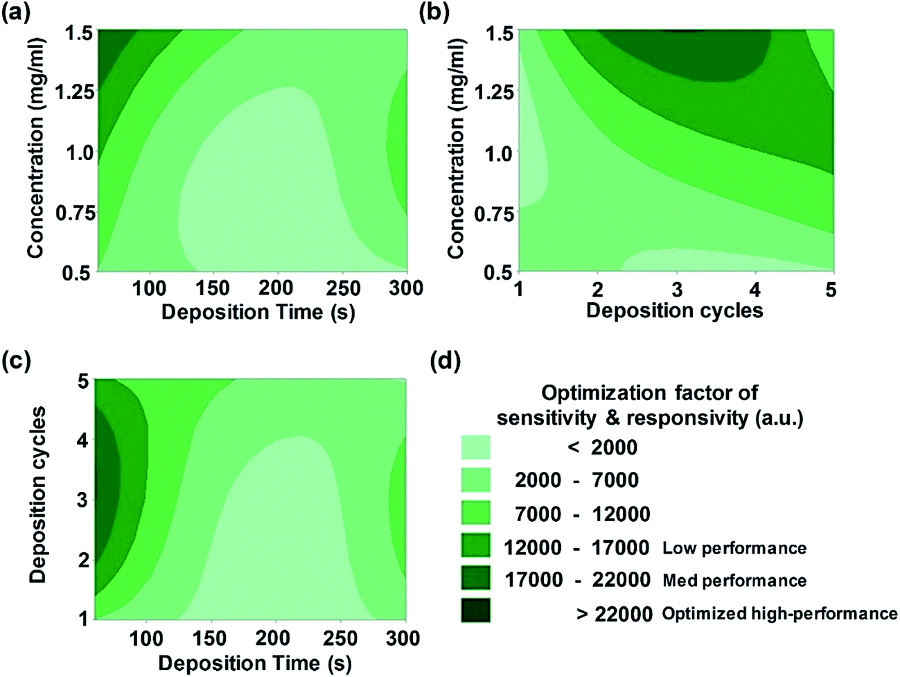 | ||
| Fig. 2 2D contour plots of mutual interactions between the fabrication parameters (a) concentration vs. deposition time, (b) concentration vs. deposition cycles, and (c) deposition cycles vs. deposition time. (d) The optimization factor is plotted in shades of green color ranges from dark green to bright green denoted as optimized high-performance (>22000 a.u.), med performance (17000–22000 a.u.), and low performance (12000–17000 a.u.), respectively. | ||
Fig. 3 shows the influence of effective control parameters (i.e., concentration, number of deposition cycles, and deposition time) on the photodetecting properties of UV sensors in which the main effect plots indicate average changes in input and output data that follows from a change in the considered level. Note that the values shown in Fig. 3 based on the Taguchi data means are the raw means of response variables for each level, whereas the fitted means employed the least squares method to predict the mean response values of a given experiment design. As shown in Fig. 3a, the sensitivity of devices increases via an increase in the concentration of secondary colloidal ZnO NRs. The increase in the density of ZnO NRs leads to the enhancement of total surface-to-volume ratio, making it more favorable for oxygen molecules to be adsorbed onto the nanostructured surfaces. It has previously been reported that the relatively large surface area of the ZnO nanostructures promotes oxygen adsorption/desorption active sites.36–38 This well-known phenomenon may increase the concentration of free mobile carriers, thereby considerably enhancing the sensitivity of the devices under UV illumination. The responsivity curve in Fig. 3a also indicates the maximum value when the concentration of the suspension is approximately 1.0 mg ml−1. However, for higher concentrations of NRs (>1.0 mg ml−1), the responsivity of the UV sensor is reduced to a mean level of approximately 2.0 A W−1. Fig. 3b indicates that the sensitivity of all sensors reached its maximum level when the number of deposition cycles was three. This is presumed to result in disordered and non-uniform deposition due to an increase in the deposition cycle exceeding the optimal value because the number of vertically aligned nanojunctions that can affect the electron transport process decreases. Additionally, the responsivity undergoes a dramatic increase of 64% with the increase in the number of deposition cycles from 1 to 5. However, increased deposition time had a destructive effect on the performance of photodetectors, as shown in Fig. 3c. This phenomenon may be attributed to the vanishing effect of ZnO nanostructured surfaces based on the accumulation of excessive colloidal ZnO NRs over the previously grown vertical ZnO NRs. The effect of the concentration of the suspension on the response/recovery times of devices is shown in Fig. 3d. Interestingly, the increase of the concentration of ZnO NRs suspension from 0.5 to 1.5 mg ml−1 significantly decreased the response/recovery time, which is favorable for typical UV detectors; the response/recovery times decreased to 55 s and 44 s at a concentration of 1.5 mg ml−1, respectively. This reduced behavior is consistent with the results obtained in previous reports.39,40 However, when the number of deposition cycles was increased beyond three, the response/recovery times increased to 55 and 65 s, respectively (Fig. 3e). In Fig. 3f, in contrast to the effect of concentration of ZnO colloidal suspension, the deposition time significantly linearly increases the mean values of the response/recovery times. In addition to these physical characteristics of the UV-sensitive semiconductor, it has also been shown that the geometry of metal electrodes could be an important factor in reducing response/recovery time.41,42
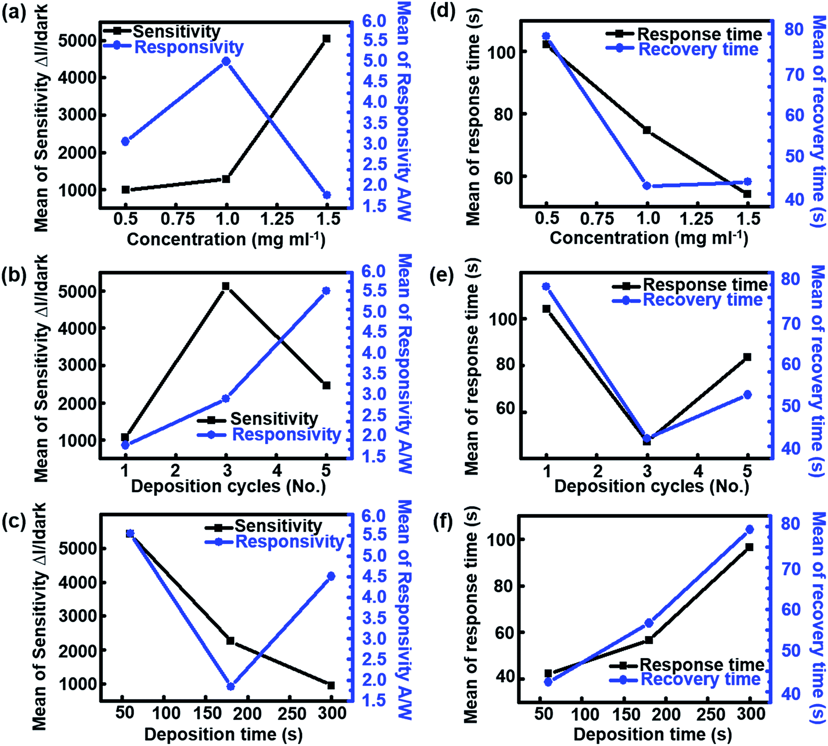 | ||
| Fig. 3 Main effect plots between fabrication parameters and UV photodetection properties. (a–c) The effect of concentration, deposition cycles, and deposition time related to UV sensitivity and responsivity, respectively. (d–f) Effect of concentration, deposition cycles, and deposition time on UV response and recovery time, respectively. | ||
Based upon the proposed experimental design, to confirm the accuracy of the model presented in Fig. 2, different samples set corresponding to the three regions in the shade of green from the contour plots were prepared in different regimes of sensing performance denoted as low (NRs-1, C1.0DC5DT60), medium (NRs-2, C1.5DC5DT180), and optimized (NRs-3, C1.5DC3DT60) performance devices, respectively (see Table S2† for more information). Fig. 4 shows the normalized photocurrent responses for each set of samples as a function of time at a UV source power of 0.345 mW cm−2 upon illumination being turned on (IUV) and off (Idark). As predicted from the contour plots, the sample of dark green region (i.e., NRs-3) has the highest photocurrent level among the sample preparation conditions. Surprisingly, the photocurrent of NR-3 (indicated by the purple line) increases by approximately 8000 times when UV was ON, showing a relatively sharp contrast to the other devices. Under the same UV irradiation, the optimally prepared photodetector has approximately 10 times higher photocurrent than that of single grown vertically aligned ZnO NRs (called bare NRs, or B-NRs). Importantly, this result is clear evidence that the deposition of the secondary layer of ZnO NRs plays an important role in obtaining superior photoconductive behavior of network-loaded ZnO NR arrays. Repeatability is another key parameter used to determine the potential capabilities of a photodetector based on our strategy. Thus, the excellent reversible switching behavior of the present double-layered ZnO NRs was tested over continuous on/off switching cycles under UV light illumination at a bias of 5.0 V. Moreover, it is noteworthy that the sensitivity level (approximately 8000) measured for our optimized device built with double-layered vertically networked ZnO is superior (or comparable) to the reported sensitivity levels for devices with various types of ZnO nanostructures such as ZnO nanowire arrays (13.8),43 ZnO nanorod/conducting polymers (100),44 graphene/ZnO NR arrays (385),45 and bridging nanosyringe structured ZnO NRs (10000).29 Thus, our device fabrication strategy is found to be a simple and robust method for improving the performance of ZnO-based UV photodetectors.
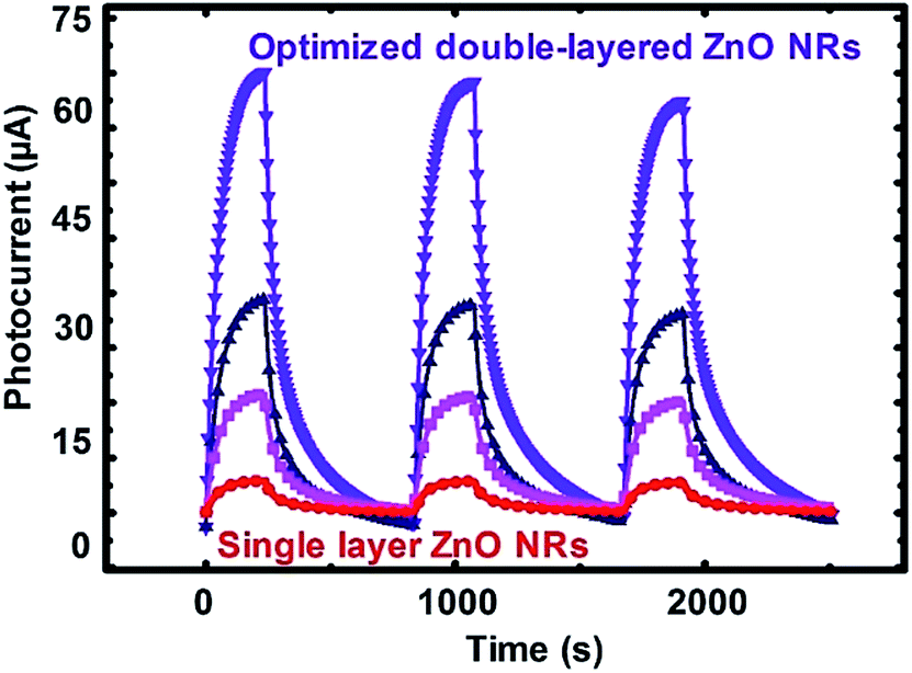 | ||
| Fig. 4 Normalized photocurrent responses as a function of time with the source power of 0.345 mW cm−2 at room temperature upon UV illumination being turned on and off. The applied bias voltage remained at 1 V for all of the measurements. Electrical response to UV exposure of single-layer ZnO NRs (red circle-line), low performance (pink square-line), med performance (navy upward triangle-line), and optimized double-layered ZnO NRs (purple downward triangle-line), respectively. | ||
To explore the correlation with the nanostructure of ZnO NRs and the performance of devices, three representative types of devices based on double-layered network-bridged ZnO NRs were observed using SEM (Fig. 5); clear configurations of secondary layers of deposited ZnO NRs were obtained (SEM images of the other samples are shown in Fig. S4†). In Fig. 5a, top-view SEM images of NRs under the conditions of a concentration of 1.0 mg ml−1, three deposition cycles, and a 60 s deposition time are shown. When the substrate was immersed in and then pulled out from the ZnO colloidal solution, the assembly of networked ZnO nanostructures started to form at the periphery of the evaporating colloidal suspension when the height of the solvent film thickness decreased to less than the diameter of the suspended ZnO NRs.30,33 The meniscus around the floating NRs in the colloidal suspension induces strong, long-range capillary forces that pull neighboring ZnO NRs together into integrated clusters (indicated by red circles in Fig. 5a),32 which leads to a less amount of deposition of networked ZnO NRs. Thus, only a small amount of vertically networked ZnO nanostructures were formed. The area most exposed to UV light had bare single-layered ZnO NRs remaining on pristine surfaces, which may be the reason for the decrease in sensing performance. Fig. 5b shows a representative SEM image of the top surface of the optimized high-performance devices, i.e., NRs-3, C1.5DC3DT60. The relatively highly concentrated ZnO NRs (i.e., 1.5 mg ml−1) traveled with the flow of fluid from the colloidal suspension to the substrate–air–liquid interface at the drying contact area as the solvent evaporates, which resulted in the formation of closely-packed uniform vertical networks, which subsequently propagated to the coating area (upper image in Fig. 5b). In contrast, the relatively large number of deposition cycles for the medium-performance device (NRs-2, C1.5DC5DT180) leads to high-density stacked-shape networks covering all of the underlying vertical ZnO NR arrays (lower SEM image in Fig. 5c). As explained earlier, at optimized experimental conditions (i.e., solution concentration and deposition time) with a continuous withdrawal speed (Fig. 1b), the floating colloidal ZnO NRs can move to all possible random orientations; however, the optimum amounts of suspended ZnO NRs are confined and deposited on the previously grown ZnO NR substrate at a tilted contact angle θ of 30°. Therefore, the secondary layer of ZnO NRs can be isotropic. However, in the highly concentrated colloidal ZnO NR condition, it becomes difficult for the ZnO NRs to align to the previously grown vertically aligned ZnO substrate because the surrounding ZnO NRs may be aggregated first, with insufficient interactions occurring during the withdrawal process. We expect that the misoriented secondary layer of colloidal ZnO NRs will undergo a phase transition into a more disordered anisotropic state that has uniaxial symmetries.46 Therefore, these specific conditions may cause the individual ZnO NRs to form close-packed bundles that have side-by-side alignments between the deposited ZnO NRs (lower image in Fig. 5c). Additionally, this accumulation might be attributed to the maximization of the entropy of the loaded networks over the vertically aligned ZnO NR arrays. It is worth noting that the organization of one dimensional (1D) nanostructures is quite different from those of nanoparticles/microspheres for which a hexagonally close-packed lattice is preferred because of the interactions of isotropic particles.47 In other words, having a large number of vacancies is more likely to occur if the deposited nanostructures originated from the shape anisotropy (i.e., a high aspect ratio of the nanorods), unlike for spherical nanoparticles, during the convective deposition process.48
 | ||
| Fig. 5 Top-view SEM images of ZnO networks deposited over the first grown ZnO NRs. (a) Low performance (NRs-1); the clusters are marked with dashed red circles, (b) optimized high-performance (NRs-3), and (c) med performance UV sensors (NRs-2). The number density of secondary ZnO NRs increased from (a) to (c); bottom images are magnified view from the selected area. | ||
When the electrical conductivity of each device was measured, the vacant geometrical factor formed in the ZnO nanostructures reduced the conductivity that affects the UV photodetection properties (Fig. 6a inset). According to the histogram in Fig. 6a, the density of secondary ZnO NRs is maximized (at approximately 215 NRs μm−2) for the medium performance device. In addition, the inset indicates that the electrical resistance of this sample is considerably more than that of other samples. This result implies that the deposition of secondary ZnO NRs beyond the optimum amount leads to degradation of the performance of the devices. The accumulation of a large number of disordered stacked-shape ZnO NRs due to increasing deposition cycles and time results in a decrease in vertical interactions between upper colloidal ZnO NRs and the as-prepared previously grown ZnO substrate, thus reducing the electrical conductivity of the samples. Furthermore, the optical transmittances (wavelengths between 250 and 800 nm) of all devices obtained using the UV-vis spectrometer are displayed in Fig. 6b, which shows the maximum transparency (approximately 95%) and approximately 100% absorbance in the visible range (wavelengths of 400 to 800 nm) and UV range (<200 nm). The sharp absorption edge implies intrinsic absorption from the direct transition of electrons assigned to semiconductors with a direct band-gap (3.37 eV). In addition, the formation of ZnO network nanostructures over the vertically aligned ZnO NR arrays shifts the absorption edge of the structure toward longer wavelengths (i.e., red shift of the absorption edge). As seen in the inset of Fig. 6b, the value of red-shift for medium performance (i.e., NRs-2) is higher than those of the other samples. Note that the fabrication condition, particularly for relatively large deposition times, leads to a very dense network of NRs, and thus, absorption of longer wavelengths of incident light.
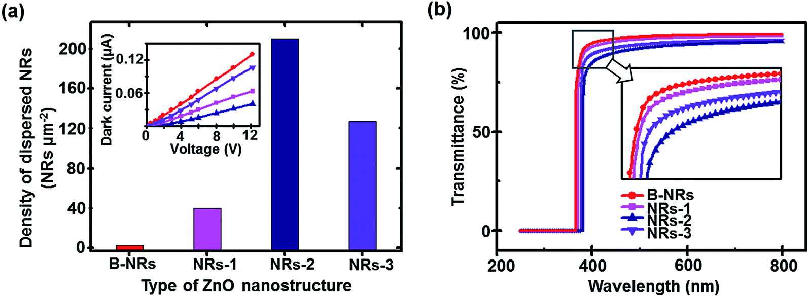 | ||
| Fig. 6 (a) Number density of secondary NRs dispersed on the vertical NR arrays. Inset graph indicates the electrical resistance of each sample. (b) Optical transmittance curve for selected samples. Details of graphs: single-layer ZnO NRs (red circle-line), low performance (pink square-line), med performance (blue upward triangle-line), and optimized double-layered ZnO NRs (purple downward triangle-line) denoted as B-NRs, NRs-1, NRs-2, NRs-3, respectively. | ||
Fig. 7 shows the XRD patterns of each set of devices. It is clear that the peaks in all of the spectra are indexed to the hexagonal wurtzite ZnO structure. It is well known that wurtzite crystal is a typical polar crystal with a dipole moment in the direction of the c-axis.49 The samples show polycrystalline characteristics with diffraction from (100), (002), (101), and (102) crystal planes. However, the intensity of the (002) plane for the NRs-2 device (C1.5DC5DT180) is significantly higher than those of the other devices, indicating the accumulation of more ZnO NRs as compared to NRs-1 (C1.0DC5DT60) and NRs-3 (C1.5DC3DT60).
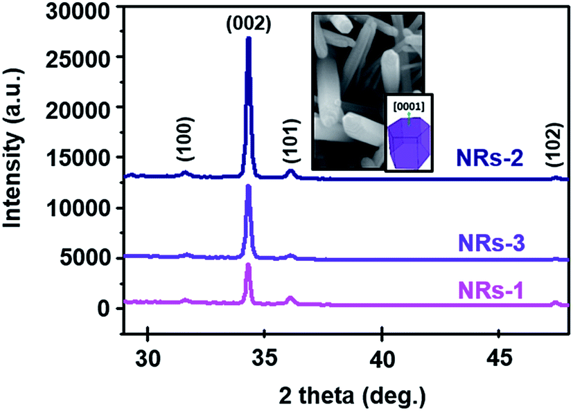 | ||
| Fig. 7 XRD patterns of three different network-loaded UV sensors; low performance, med performance, and optimized high-performance, denoted as NRs-1, NRs-2, NRs-3, respectively. The enhancement of (002) peak intensity shows the increase in secondary NR number density. Inset: top-view SEM image of hexagonal structure of ZnO nanonetwork. | ||
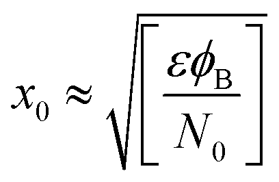
To understand the mechanism of the UV photodetection process, it is important to note that oxygen molecules adsorb on the surface of ZnO NRs, thereby trapping free electrons and becoming negatively charged ions when the ZnO network-arrays are placed in the dark (without UV illumination). This process leads to the formation of a depletion layer near the surface of the individual ZnO NRs. Generally, when the energy of incident UV photons is greater than the bandgap energy of ZnO NRs, a large number of hole–electron pairs is generated. The photogenerated holes migrate to the surface along the potential gradient formed by the band bending while the oxygen atoms are desorbed from the surface, thus weakening the depletion region. At the same time, the electrons contribute to the conduction process and increase the conductivity.50 According to previous reports, the lack of inter-nanorod junctions in vertically aligned ZnO NR arrays results in low sensitivity and high response/recovery times, which are the main obstacles for such devices.28,29 Here, we assume that the accumulation of secondary networked ZnO NRs on the surface of vertical NRs contributes to the formation of nanojunctions acting as energy barriers; these nanojunctions play a significant role in enhancing the UV sensing properties of the detector. Fig. 8 shows the junctions formed between networks and NR arrays and a representative SEM image. The band diagram indicates that the illumination of UV light causes the energy barrier of the junctions to decrease. In this case, the conductance is dominated by these junction barriers, which can be treated as two back-to-back Schottky barriers. The relatively fast UV response/recovery time can be attributed to easy electron tunneling and transportation via lowered barriers upon UV illumination in junctions, which is equal to the lowering of the effective barrier height. The geometry of the energy bands near the planar charged interface is calculated using the Schottky approximation from Poisson's equation (eqn (1) and (2)):37,45
 | (1) |
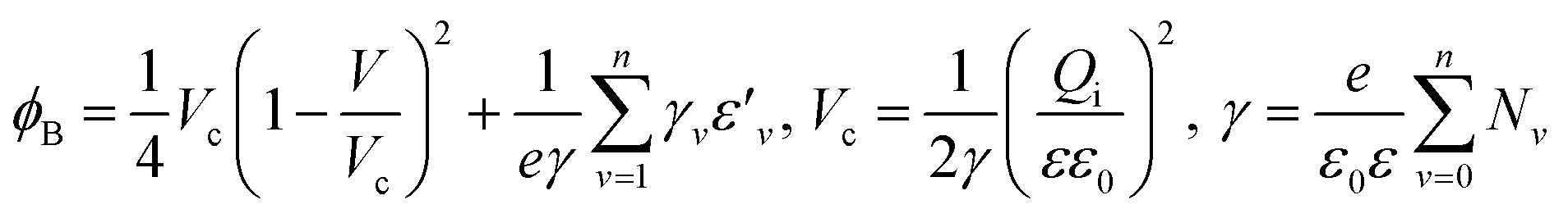 | (2) |
 | (3) |
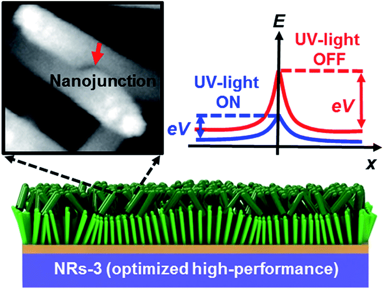 | ||
| Fig. 8 Schematic depiction of junctions in nanoscale formed within ZnO networks; optimized density ZnO networks located over the first grown vertically-aligned ZnO NRs. Inset is a representative SEM image of nanojunction between the ZnO NRs (left) and the energy diagram for each UV light on and off state (right). | ||
Therefore, eqn (4) gives the width of the depletion area:
 | (4) |
Eqn (3) and (4) clearly indicate that the barrier height formed at the inter-connected nanojunctions is decreased upon UV illumination, thus promoting a faster sensing process with high detectability. Therefore, electrical conduction in percolated networks of NRs is dominated by the nanojunction barriers, which are not readily available in as-grown vertically aligned ZnO NR devices. Previous studies of nanojunctions also revealed the dominant effect of the resistance of the junction barrier.51 Note that light-induced modulation of the barrier height occurs much faster than the oxygen diffusion or trap-discharging processes. Consequently, the dominant influence of the effective junction barrier would lead to a fast response and recovery time.23,51 The denser the network, the more junctions can be made between ZnO NRs. Therefore, we believe that the UV photodetection performance strongly depends on the type of such junctions and the height of the energy barriers.52 Chen et al.53 previously showed that the junction barriers formed by these networks hindered the transfer of electrons between neighboring ZnO NRs because the electric current must pass through the formed depletion regions. The optimized high-performance hierarchical networked nanostructure (NRs-3, C1.5DC3DT60) obtained using Taguchi-method-based carefully controlled experimental conditions provided a unique compact layer of ZnO networks on the vertically grown ZnO NR arrays. The increase in the electrical resistance of the samples due to the larger number of deposition cycles (i.e., NRs-2, C1.5DC5DT180) reduces the UV sensing capability by causing highly disordered stacking of ZnO NRs, which also prohibits the impact of UV-excited released electrons from vertically grown ZnO NRs based on the shadow effect.
4. Conclusions
In summary, we have developed a simple and robust method for fabricating network-loaded ZnO NRs arrays for use in a UV photodetector. Systematically determined sets of fabrication parameters obtained using Taguchi experimental design and the careful control of the secondary layer of ZnO NRs proposed here leads to an optimized UV sensory material platform with a significantly improved sensitivity of approximately 8000. Moreover, this well-configured method enabled us to optimize sensitivity, responsivity, and response/recovery time with the minimum possible number of experiments in a cost-effective way. As a conclusion, the origin of the enhanced UV sensing performance was clearly attributed to the unique geometrical characteristics of vertically network-bridged ZnO nanostructures, as compared to the pristine as-grown ZnO NRs arrays. Furthermore, the enhancement of sensitivity was primarily due to the increase in surface-to-volume ratio within the double-layered ZnO NR configuration, which increased the concentration of free charge carriers by lowering the junction barriers. Our approach to the optimized network-loaded ZnO nanostructure has great potential in further study of various sensor applications.Acknowledgements
This research was supported by a grant from the University of Kashan (Grant No. 159023/64) and this work was also supported by National Research Foundation of Korea Grant funded by the Korean Government (NRF-2014R1A1A2058350, NRF-2017R1A2B4007483).References
- E. Monroy, F. Omnes and F. Calle, Semicond. Sci. Technol., 2003, 18, 33–51 CrossRef.
- H. Kind, H. Q. Yan, B. Messer, M. Law and P. D. Yang, Adv. Mater., 2002, 14, 158–160 CrossRef CAS.
- R. A. Yotter and D. M. Wilson, IEEE Sens. J., 2003, 3, 288–303 CrossRef CAS.
- P. Sharma, K. Sreenivas and K. V. Rao, J. Appl. Phys., 2003, 93, 3963–3970 CrossRef CAS.
- G. Konstantatos and E. H. Sargent, Nat. Nanotechnol., 2010, 5, 391–400 CrossRef CAS PubMed.
- Y. Xia, P. Yang, Y. Sun, Y. Wu, B. Mayers, B. Gates, Y. Yin, F. Kim and H. Yan, Adv. Mater., 2003, 15, 353–389 CrossRef CAS.
- C. M. Lieber, Solid State Commun., 1998, 107, 607–616 CrossRef CAS.
- X. Liu, L. Gu, Q. Zhang, J. Wu, Y. Long and Z. Fan, Nat. Commun., 2014, 5, 4007 CAS.
- O. Lupan, V. Cretu, V. Postica, M. Ahmadi, B. R. Cuenya, L. Chow, I. Tiginyanu, B. Viana, T. Pauporté and R. Adelung, Sens. Actuators, B, 2016, 223, 893–903 CrossRef CAS.
- Y. Li, T. Tokizono, M. Liao, M. Zhong, Y. Koide, I. Yamada and J.-J. Delaunay, Adv. Funct. Mater., 2010, 20, 3972–3978 CrossRef CAS.
- X. Fang, Y. Bando, M. Liao, U. K. Gautam, C. Zhi, B. Dierre, B. Liu, T. Zhai, T. Sekiguchi, Y. Koide and D. Golberg, Adv. Mater., 2009, 21, 2034–2039 CrossRef CAS.
- S. Park, S. An, H. Ko, S. Lee and C. Lee, Sens. Actuators, B, 2013, 188, 1270–1276 CrossRef CAS.
- X. Wang, Y. Zhang, X. Chen, M. He, C. Liu, Y. Yin, X. Zou and S. Li, Nanoscale, 2014, 6, 12009–12017 RSC.
- F. Fleischhaker, V. Wloka and I. Hennig, J. Mater. Chem., 2010, 20, 6622–6625 RSC.
- J. Guo, J. Zhang, M. Zhu, D. Ju, H. Xu and B. Cao, Sens. Actuators, B, 2014, 199, 339–345 CrossRef CAS.
- D.-M. Shin, E. L. Tsege, S. H. Kang, W. Seung, S.-W. Kim, H. K. Kim, S. W. Hong and Y.-H. Hwang, Nano Energy, 2015, 12, 268–277 CrossRef CAS.
- D.-Y. Guo, C.-X. Shan, S.-N. Qu and D.-Z. Shen, Sci. Rep., 2014, 4, 7469 CrossRef CAS PubMed.
- Z. L. Wang, J. Phys.: Condens. Matter, 2004, 16, R829–R858 CrossRef CAS.
- Z. L. Wang, Mater. Today, 2004, 7, 26–33 CrossRef CAS.
- A. Moulahi and F. Sediri, Ceram. Int., 2014, 40, 943–950 CrossRef CAS.
- B. Nikoobakht, X. Wang, A. Herzing and J. Shi, Chem. Soc. Rev., 2013, 42, 342–365 RSC.
- W. Tian, H. Lu and L. Li, Nano Res., 2015, 8, 382–405 CrossRef CAS.
- Y. K. Mishra, G. Modi, V. Cretu, V. Postica, O. Lupan, T. Reimer, I. Paulowicz, V. Hrkac, W. Benecke, L. Kienle and R. Adelung, ACS Appl. Mater. Interfaces, 2015, 7, 14303–14316 CAS.
- N. Logothetis and H. P. Wynn, Quality through design: experimental design, off-line quality control, and Taguchi's contributions, Oxford University Press, 1990 Search PubMed.
- K. J. Rao and S. Paria, ACS Sustainable Chem. Eng., 2015, 3, 483–491 CrossRef CAS.
- Y.-D. Chiang, H.-Y. Lian, S.-Y. Leo, S.-G. Wang, Y. Yamauchi and K. C.-W. Wu, J. Phys. Chem. C, 2011, 115, 13158–13165 CAS.
- R. K. Roy, Design of experiments using the Taguchi approach: 16 steps to product and process improvement, Wiley, 2001 Search PubMed.
- S. F. Akhtarianfar, A. Khayatian and M. Almasi-Kashi, Ceram. Int., 2016, 42, 13421–13431 CrossRef CAS.
- M. R. Alenezi, S. J. Henley and S. Silva, Sci. Rep., 2015, 5, 8516 CrossRef PubMed.
- S. W. Hong, W. Jeong, H. Ko, M. R. Kessler, V. V. Tsukruk and Z. Lin, Adv. Funct. Mater., 2008, 18, 2114–2122 CrossRef CAS.
- S. W. Hong, J. Xia and Z. Lin, Adv. Mater., 2007, 19, 1413–1417 CrossRef CAS.
- S. H. Kang, W. S. Hwang, Z. Lin, S.-H. Kwon and S. W. Hong, Nano Lett., 2015, 15, 7913–7920 CrossRef CAS PubMed.
- D. G. Bae, J.-E. Jeong, S. H. Kang, M. Byun, D.-W. Han, Z. Lin, H. Y. Woo and S. W. Hong, Small, 2016, 12, 4254–4263 CrossRef CAS PubMed.
- L. Guo, H. Zhang, D. Zhao, B. Li, Z. Zhang, M. Jiang and D. Shen, Sens. Actuators, B, 2012, 166, 12–16 CrossRef.
- Y. Li, X. Dong, C. Cheng, X. Zhou, P. Zhang, J. Gao and H. Zhang, Phys. B, 2009, 404, 4282–4285 CrossRef CAS.
- L. Ji, S. Peng, Y.-K. Su, S.-J. Young, C. Wu and W. Cheng, Appl. Phys. Lett., 2009, 94, 203106 CrossRef.
- N. Liu, G. Fang, W. Zeng, H. Zhou, F. Cheng, Q. Zheng, L. Yuan, X. Zou and X. Zhao, ACS Appl. Mater. Interfaces, 2010, 2, 1973–1979 CAS.
- F.-H. Wang and C.-E. Tsai, IEEE J. Sel. Top. Quantum Electron., 2016, 23, 3800606 Search PubMed.
- R. Azimirad, A. Khayatian, M. A. Kashi and S. Safa, J. Sol-Gel Sci. Technol., 2014, 71, 540–548 CrossRef CAS.
- S. Hullavarad, N. Hullavarad, P. Karulkar, A. Luykx and P. Valdivia, Nanoscale Res. Lett., 2007, 2, 161–167 CrossRef CAS.
- C.-Y. Lu, S.-P. Chang, S.-J. Chang, T.-J. Hsueh, C.-L. Hsu, Y.-Z. Chiou and I.-C. Chen, Semicond. Sci. Technol., 2009, 24, 075005 CrossRef.
- J. Suehiro, N. Nakagawa, S. Hidaka, M. Ueda, K. Imasaka, M. Higashihata, T. Okada and M. Hara, Nanotechnology, 2006, 17, 2567–2573 CrossRef CAS PubMed.
- Y. H. Leung, Z. He, L. Luo, C. Tsang, N. Wong, W. Zhang and S. T. Lee, Appl. Phys. Lett., 2010, 96, 053102 CrossRef.
- O. Game, U. Singh, T. Kumari, A. Banpurkar and S. Ogale, Nanoscale, 2014, 6, 503–513 RSC.
- B. Nie, J. G. Hu, L. B. Luo, C. Xie, L. H. Zeng, P. Lv, F.-Z. Li, J.-S. Jie, M. Feng, C.-Y. Wu, Y.-Q. Yu and S.-H. Yu, Small, 2013, 9, 2872–2879 CrossRef CAS PubMed.
- A. R. Tao, J. Huang and P. Yang, Acc. Chem. Res., 2008, 41, 1662–1673 CrossRef CAS PubMed.
- P. Yang and F. Kim, ChemPhysChem, 2002, 3, 503–506 CrossRef CAS PubMed.
- N. D. Denkov, O. D. Velev, P. A. Kralchevsky, I. B. Ivanov, H. Yoshimura and K. Nagayama, Nature, 1993, 361, 26 CrossRef.
- L.-L. Yang, Q. Zhao, M. Willander and J. Yang, J. Cryst. Growth, 2009, 311, 1046–1050 CrossRef CAS.
- C. Liu, B. Zhang, Z. Lu, N. Binh, K. Wakatsuki, Y. Segawa and R. Mu, J. Mater. Sci.: Mater. Electron., 2009, 20, 197–201 CrossRef CAS.
- C. Yan, N. Singh, H. Cai, C. L. Gan and P. S. Lee, ACS Appl. Mater. Interfaces, 2010, 2, 1794–1797 CAS.
- D. Gedamu, I. Paulowicz, S. Kaps, O. Lupan, S. Wille, G. Haidarschin, Y. K. Mishra and R. Adelung, Adv. Mater., 2014, 26, 1541–1550 CrossRef CAS PubMed.
- C.-Y. Chen, M.-W. Chen, C.-Y. Hsu, D.-H. Lien, M.-J. Chen and J.-H. He, IEEE J. Sel. Top. Quantum Electron., 2012, 18, 1807–1911 CrossRef CAS.
Footnote |
| † Electronic supplementary information (ESI) available. See DOI: 10.1039/c7ra04773h |
| This journal is © The Royal Society of Chemistry 2017 |