DOI:
10.1039/C7RA04477A
(Paper)
RSC Adv., 2017,
7, 28124-28129
Thermal spin current in zigzag silicene nanoribbons with sp2–sp3 edges
Received
20th April 2017
, Accepted 20th May 2017
First published on 26th May 2017
Abstract
Using first-principles calculations combined with non-equilibrium Green's function method, we study thermal spin transport of zigzag silicene nanoribbons (ZSiNRs) with unsymmetrical sp2–sp3 edges under a temperature gradient but no bias. Both in the linear and non-linear response regimes, we have opposite flow directions for different spins, which leads unambiguously to spin current. Most important is that pure spin current can be achieved and basically no tuning of the chemical potential μ is needed since the neutral point is very close to μ = 0 (the chemical potential located at the Fermi level) and this fact holds for a very large temperature range studied (110 ≤ TL ≤ 300 K). The direction of charge current induced by a temperature gradient can be easily reversed by tuning the chemical potential, while the spin current is almost unchanged in the same process, indicating that the spin current is robust and stable. In addition, both spin current and charge current present a thermoelectric diode behavior for TL ≤ 200 K in the nonlinear response regime. These findings suggest that the unsymmetrically sp2–sp3 terminated ZSiNRs are promising materials for spin caloritronic devices.
1 Introduction
Spin caloritronics, a combination of spintronics and thermoelectrics to study interaction among spin, charge and heat, has attracted great attention in recent years.1,2 One of the most important observations in spin caloritronic experiments is the spin-dependent Seebeck effect, which features different Seebeck coefficients for different spins in spin polarized systems.3–5 Such an effect provides a good way for controlling the electron spins by temperature gradient and may be well utilized in spintronics. It is well known that spin current, a very important physical quantity in spintronics, is characterized by opposite flow directions of the different spins.6 Very interestingly, spin-dependent Seebeck effect in certain systems may lead to Seebeck coefficients with different signs for different spins, which drives different spins to flow in opposite directions. Therefore, it offers an alternative method to generate spin current. From this, we see that the key to create spin current using a temperature gradient is to find suitable spin-thermoelectric materials, which holds Seebeck thermopower with opposite signs for different spins.
Two-dimensional (2D) materials with atomic thickness have initiated great interests since the discovery of graphene,7 and a large number of new 2D materials are emerging very quickly, such as hexagonal boron-nitride sheet,8 transition metal dichalcogenides,9 black phospherene,10 borophene,11 2D SiS layers,12 and many others.13–17 In particular, silicene, a hexagonal atomic structure with two sublattices displaced vertically, forming a sp3-like hybridization of silicon atoms, was proposed theoretically18 and its structural stability was later proved with phonon spectra calculations by several groups.19–21 Now silicene has been synthesized experimentally.22 Moreover, many interesting properties, such as spin Seebeck effects,23 spin filter effect,24 quantum spin Hall effect,25,26 etc., have been observed in silicene or corresponding nanoribbons. First-principle calculations have shown that silicene is very reactive and can be easily functionalized with hydrogen.27 Especially, zigzag silicene nanoribbons (ZSiNRs) with asymmetric H-terminations, namely, with a sp2 edge (each edge C atom saturated by one H atom) and a sp3 edge (each edge C atom saturated by two H atoms) and abbreviated as H–2H ZSiNRs, exhibit bipolar magnetic semiconducting behavior and it is good for study in spin caloritronics.28,29 Compared with other forms of hydrogenated silicene nanoribbons, H–2H ZSiNRs have many excellent properties beneficial for spintronic applications, such as stable ferromagnetic (FM) ground state, flat valence and conduction bands with different spins.
In this work, we investigate its thermal spin transport performance. In detail, by utilizing density functional calculations and a non-equilibrium Green's function technique, we study spin thermoelectric effect for both linear and non-linear response regimes in H–2H ZSiNRs by taking a 6-ZSiNR as an example. The results show that the flow directions of the spin up and down currents are opposite when a temperature gradient is applied between the left and right leads. This gives rise to spin current unambiguously. More interestingly, pure spin current can be induced by tuning the system's chemical potential and the temperature of the leads. In addition, spin-Seebeck diode behavior,30,31 in which the spin current is driven by a negative temperature gradient between two leads but not by a positive one, can be realized in this device.
2 Methodology
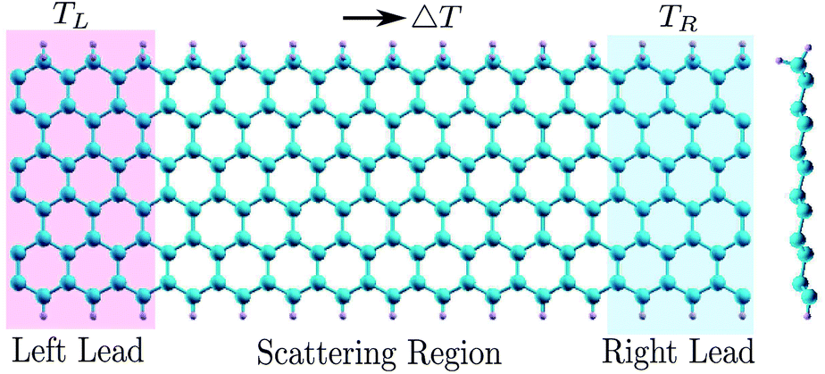
The model device in the study is constructed by an infinite H–2H 6-ZSiNR, which is divided into three regions: left lead, right lead and scattering region (shown in Fig. 1). The left and right leads are kept at different temperatures, respectively. The temperature gradient formed between the two leads may drive a current, depending on the difference of transmission probabilities of the electrons and holes in the system. We study under what conditions can we realize opposite currents for different spins, which is a necessity of generating spin current.
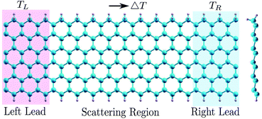 |
| | Fig. 1 The device structure is divided into three parts: left lead, right lead and scattering region. The right part of the figure is the side view of the H–2H 6-ZSiNR. ‘H–2H’ indicates asymmetric hydrogen terminations on the ribbon edges, which correspond to the sp2–sp3 edges. TL and TR are the temperatures of the left and right leads. The temperature gradient is defined as ΔT = TL − TR. | |
Calculations for the electronic structure and spin transport are performed by the Nanodcal package,32 which combines density functional theory (DFT) and non-equilibrium Green's function (NEGF) for quantum transport study. A double zeta polarized (DZP) basis set is adopted for describing the electron wave function, and the generalized gradient approximation (GGA) with Perdew–Burke–Ernzerhof (PBE)33 parametrization is applied for the exchange-correlation potential. The vacuum layer is set to 16 Å to avoid inter-layer interaction. Moreover, the energy cutoff is 200 Ry and the mesh grid of the electrodes in 1D Brillouin zone (BZ) is 1 × 1 × 100. The structure is fully relaxed by a conjugate gradient method until the residual force on each atom is less than 0.01 eV Å−1.
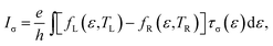
According to the Landauer–Büttiker formula, the spin-dependent electric current and heat current are given by34,35
| |
 | (1) |
| |
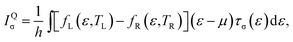 | (2) |
where
e is the electron charge,
h is the Planck constant, and
τσ(
ε) is the spin-dependent transmission coefficient calculated by
| | |
τσ(ε) = Γr[ΓL(ε)Gr(ε)ΓR(ε)Ga(ε)]σσ.
| (3) |
Here, σ is the spin index (
σ = ↑,↓).
Γα (α = L,R) is the linewidth function describing the coupling between lead α and the scattering region;
Gr (
Ga) is the retarded (advanced) Green's function;
fα and
Tα are the Fermi distribution function and temperature of the α lead, respectively. A finite
fL −
fR due to a temperature gradient Δ
T =
TL −
TR may lead to a different current for different spins, depending on the feature of the spin polarized transmission functions.
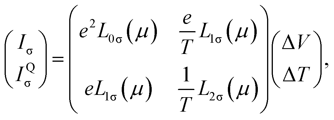
In the linear response regime with the bias voltage ΔV ≪ Vα and ΔT ≪ Tα, the current Iσ and heat current IQσ can be written in the matrix form as35
| |
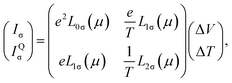 | (4) |
where
| |
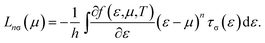 | (5) |
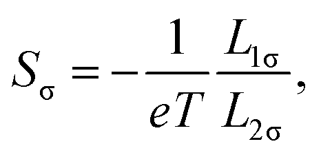
Then the spin-dependent Seebeck coefficients Sσ and the spin-dependent electrical conductance Gσ can be obtained by
| |
 | (6) |
The spin and charge Seebeck coefficients are defined by SS = S↑ − S↓ and Sc = S↑ + S↓, respectively. The coefficient SS reflects the possibility of the device to induce spin current by temperature gradient.
3 Results and discussion
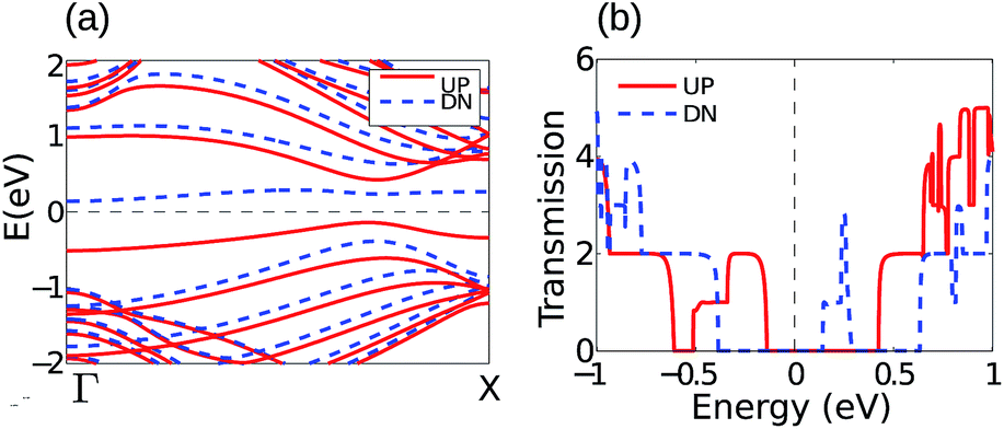
First, we investigate the lead band structure and equilibrium transport properties of the H–2H 6-ZSiNR device shown in Fig. 1 before moving to study the temperature gradient induced effects. The lead band structure is shown in Fig. 2(a), from which we see that H–2H 6-ZSiNR is a spin semiconductor characterized by a spin gap, namely, a gap determined by a spin up valence band and a spin down conduction band. Fig. 2(b) shows the spin-resolved transmission function of H–2H 6-ZSiNR, which is consistent with the result from the band-counting method,36 namely, the transmission is always equal to the number of bands at each energy. In the following, we investigate the spin thermoelectric effect in this device both in linear and non-linear response regimes.
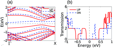 |
| | Fig. 2 Spin-polarized band structure (a) and transmission function (b) of the H–2H ZSiNR in the FM state. | |
3.1 Linear response regime
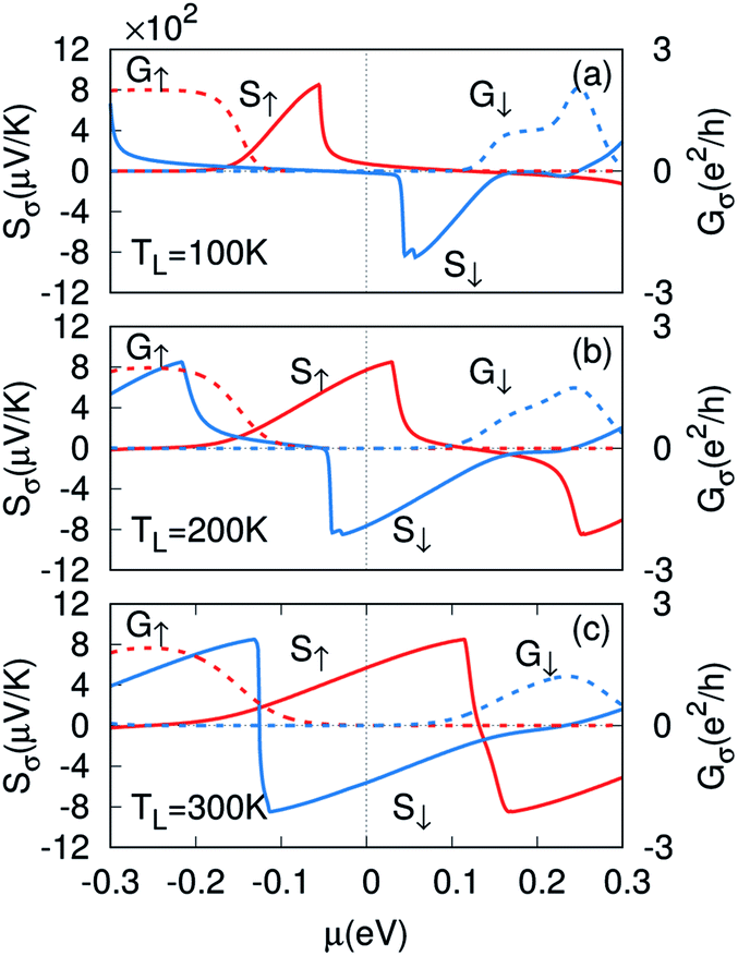
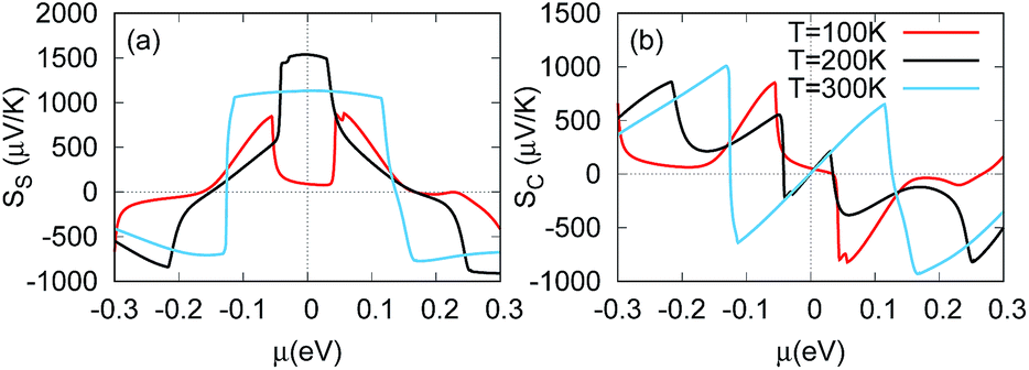
For H–2H 6-ZSiNR, a striking feature is the asymmetric transmission functions for the two spins around the Fermi level, and it clearly shows that the spin up (spin down) transport channel is dominated by p-type (n-type) carriers (see Fig. 2), which is promising, as shown below, for generating spin current in spin caloritronics. In Fig. 3, we present the spin-dependent Seebeck thermopower and conductance versus chemical potential at TL = 100, 200 and 300 K in the linear response regime (ΔT ≪ TL), respectively. It is found that the signs of S↑ and S↓ are opposite around the Fermi level. This is easy to understand. From eqn (4) and (5), the Sσ has two contributions, one from the holes (the integration part with ε − μ ≤ 0) and the other from the electrons (the part with ε − μ ≥ 0). The holes contribute a positive part while the electrons contribute a negative part. Obviously, from Fig. 2, the spin up channel is dominated by holes while the spin down channel by electrons, thus we have S↑ > 0 and S↓ < 0 around μ = 0. The opposite signs of S↑ and S↓ indicate that thermal spin voltage is induced and different spins will be driven to the opposite side of the device by a temperature gradient.
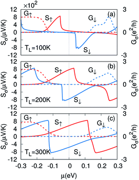 |
| | Fig. 3 Spin-dependent Seebeck thermopower and thermal conductance as a function of chemical potential for: (a) TL = 100 K, (b) TL = 200 K, (c) TL = 300 K. Solid (dash) line is for Sσ (Gσ). μ = 0 means the chemical potential located at the Fermi level. | |
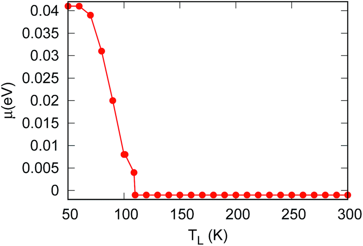
More interestingly, we can always find a neutral point around μ = 0 where S↑ + S↓ = 0 and contributions from electrons and holes cancel with each other.37 At this point, the charge voltage (Vc = ScΔT) is zero but a finite spin voltage (Vs = SsΔT ≠ 0) is produced in open-circuit condition. The position (the μ value) of the neutral point around μ = 0 as a function of lead temperature is shown in Fig. 4. It shows that when T ≥ 110 K, the neutral point is always at μ = −0.001 eV, which is negligibly small and demonstrates no need of tuning the chemical potential in generating pure spin current. Thus, this material is potentially useful for fabricating pure spin current devices based on spin-dependent Seebeck effect.
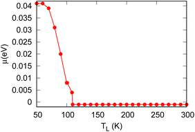 |
| | Fig. 4 The position of the neutral point around the Fermi level as a function of lead temperature. | |
Fig. 5 shows the spin and charge Seebeck coefficient as a function of chemical potential for different temperatures. For T = 200 and 300 K, the spin Seebeck coefficient is approximately an even function of chemical potential, while the charge Seebeck coefficient is basically an odd function and SC is exactly zero at μ ≈ −0.001 eV. It is very interesting that net electronic current driven by a temperature gradient in this system can be easily modulated to flow from the high temperature side to the low temperature side, or vice versa, by tuning the chemical potential (see Fig. 5(b)). Meanwhile, there is a platform in the spin Seebeck coefficient around μ = 0 (see Fig. 5(a)), indicating that the spin voltage is robust and stable, almost unchanged with the chemical potential in a certain range.
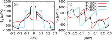 |
| | Fig. 5 (a) Spin Seebeck thermopower and (b) charge Seebeck thermopower as a function of chemical potential for different values of temperature. | |
3.2 Non-linear response regime
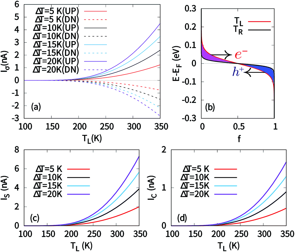
It is seen clearly from Fig. 3 that even at high temperature (TL = 110 and 300 K), the thermal conductance is always negligibly small, which will give rise to a negligible spin current and charge current by a small temperature gradient. This arises from the large spin gap in 6-ZSiNR. It will only result in spin accumulation at opposite sides of the device,37 but not in a steady and considerable spin current. One way to increase the current is to increase the temperature gradient ΔT, which will go beyond the linear response regime. Thus, next, we will discuss the non-linear response regime where ΔT ≪ TL is not satisfied. Under this condition, all discussions will be based on the current calculated directly by eqn (1). Fig. 5(a) shows the spin-dependent currents of H–2H 6-ZSiNR versus ΔT for various TL. It is clearly seen that spin-up and spin-down currents flow in opposite direction, indicating that there is spin-dependent Seebeck effect in H–2H 6-ZSiNR. As TL increases, the sign of I↑ and I↓ is always opposite for all values of ΔT, indicating that spin-dependent Seebeck effect is stable in this system. Consequently, it is natural that the magnitude of the thermal spin current is always larger than that of charge current (see Fig. 6(c) and (d)).
 |
| | Fig. 6 (a) Spin-dependent currents versus left lead temperature TL for ΔT = 5, 10, 15 and 20 K. (b) The Fermi distribution of the left lead (hot side) and the right lead (cold side). Current is generated due to the Fermi distribution difference of the left and right leads. (c) The spin current and (d) charge current versus TL for different ΔT. | |
To further make clear the fundamental reason behind these interesting features, we plot the electron distribution function of the left and right leads as shown in Fig. 6(b), where we suppose TL > TR. We obtain Δf (E) = fL (E) − fR (E) as an odd function around the Fermi level. The imbalance in Fermi distribution arising from different temperatures at the two sides allows net electrons and holes flow in opposite directions. It can be seen from the spin-dependent transmission spectra [see Fig. 1(c)] that, there is a n-type spin-down channel above the Fermi level and a p-type spin-up channel below the Fermi level, which breaks the electron–hole symmetry. Thus, the spin-up holes move left and spin-down electrons move right. This is consistent with the positive spin up current and the negative spin down current in Fig. 6(a).
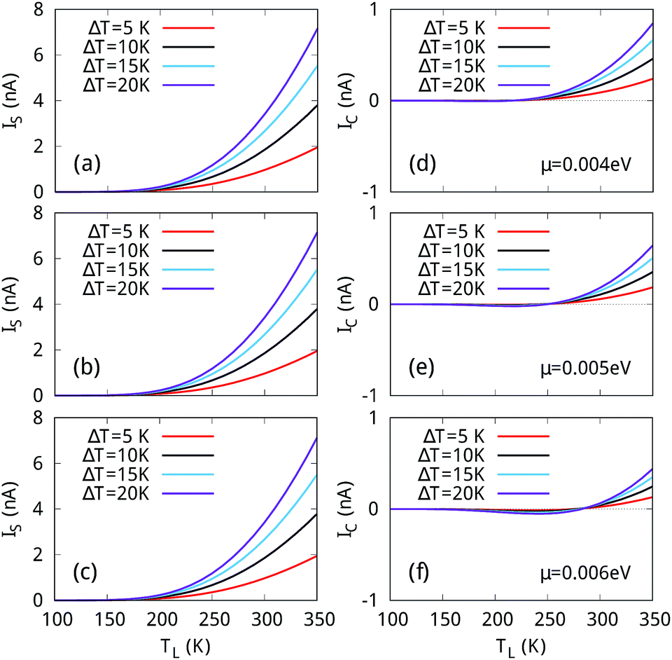
However, Fig. 6(c) and (d) show that the spin-dependent Seebeck effect is not perfect in the device for producing pure spin current since the magnitude of the spin-up current is always larger than that of the spin-down current. According to the characteristics of the band structure and transmission spectra, we study the effects of different chemical potentials on the spin current IS and charge current IC versus TL and the results at three values of chemical potentials are plotted in Fig. 7. For μ = 0.004 eV [see in Fig. 7(a) and (d)], pure spin current is generated in the range of 130 ≤ TL ≤ 230 K for all values of ΔT. This is because with the chemical potential μ increasing from EF to μ = 0.004 eV, the contribution of spin-down electrons increases, leading to I↑ = −I↓. As μ further increases, the range of temperature producing pure spin current increases (see Fig. 7(b, c) and (e, f)).
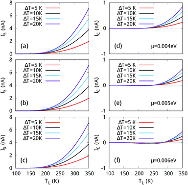 |
| | Fig. 7 The spin current (a–c) and charge current (d–f) versus the temperature of the left lead TL at different chemical potentials μ. | |
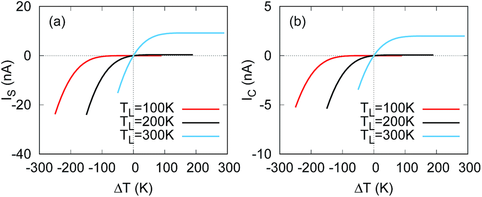
Next, we investigate IS and IC versus ΔT polarity at different TL. Fig. 8 illustrates that both spin current and charge current present a thermoelectric diode behavior for TL ≤ 200 K, allowing spin current IS and IC to only occur for a positive temperature gradient. This can be understood as follows. As indicated in eqn (1), the current is determined by both the transmission τσ and the difference Δf between the Fermi distribution functions fL and fR of the two leads. Further, fL and fR are dependent on the lead temperatures TL and TR. For a fixed TL which is so low (like 100 K or 200 K) that the rapidly changing area of fL is inside the gap, when TR < TL, namely, ΔT > 0 since ΔT is defined as TR − TL, the slope of fR around the Fermi level will be larger than that of fL and the finite Δf mainly arises from the gap region (like the case in Fig. 6(b)) where the transmission is zero. Thus, the current is negligible. However, when TR > TL, the slope of fR around the Fermi level will be smaller than that of fL, so fR will be much smoother and the Δf may extend wide enough to cover the valence band and the conduction band regions where the transmission is large when TR is high enough. Thus the current can be much larger. This results in the diode behavior in both the spin current and the charge current. Nevertheless, if TL is high enough so that the rapidly changing area of fL extends to the valence and conduction band region, both a positive or a negative ΔT main lead to a finite current since the Δf always covers the high transmission region, namely, the valence and conduction band regions. Consequently, the diode behavior may disappear with the increase of temperature of both leads.
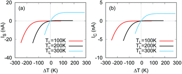 |
| | Fig. 8 The spin current (a) and charge current (b) versus ΔT with different polarity for TL = 100, 200 and 300 K. | |
3.3 The ribbon width effect
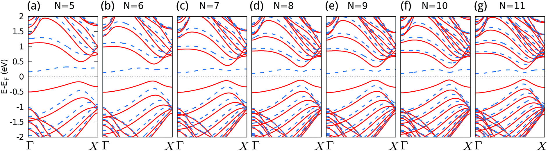
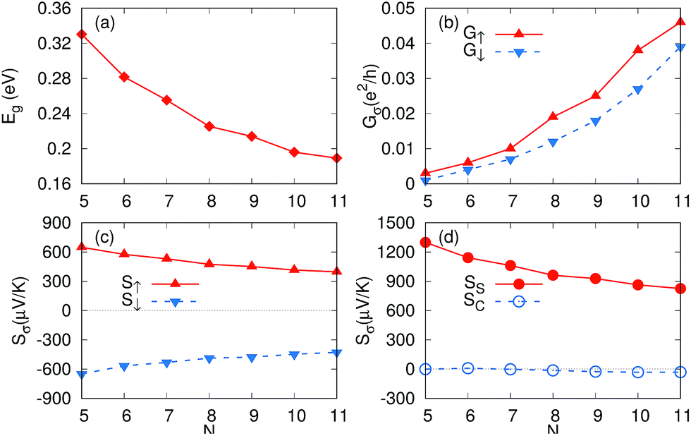
The thermal spin current and thermoelectric diode behaviors highly depend on the spin semiconductor characteristics which may be affected by the nanoribbon width. Thus it is necessary to study the electronic structure of 2H–H ZSiNRs with different widths. Fig. 9(a–g) show the band structures of ferromagnetic 2H–H N-ZSiNRs as a function of ribbon width (N = 5–11) and they look very similar. We find that there is always a spin gap for different ribbon widths and the size of the spin gap Eg decreases monotonously as N increases (see Fig. 10(a)).
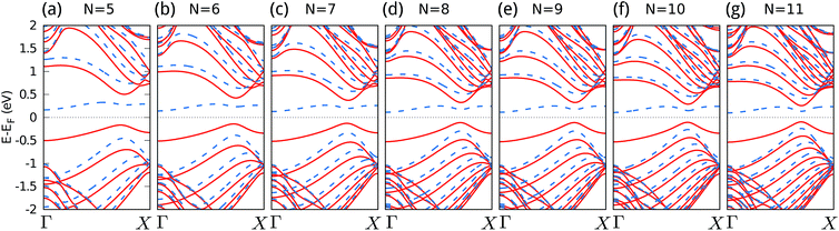 |
| | Fig. 9 (a)–(g) The band structure of the ferromagnetic 2H–H N-ZSiNRs with different ribbon widths, where N denotes the number of ziazag-like lines across the ribbon width. The red solid line denotes the spin-up channel while the blue dash line denotes the spin-down channel. | |
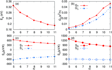 |
| | Fig. 10 (a) The spin gap; (b) the spin-dependent conductance; (c) the spin-dependent Seebeck thermopower; (d) the spin Seebeck thermopower and charge Seebeck thermopower as a function of ribbon width at the Fermi level with T = 300 K. | |
In order to see more clearly the ribbon width effect, the spin-dependent conductance (G↑, G↓), spin-dependent Seebeck thermopower (S↑, S↓), spin Seebeck thermopower SS and charge Seebeck thermopower Sc versus the ribbon widths have also been investigated. Their values at μ = 0 with T = 300 K are shown in Fig. 10(b–d). The spin-dependent conductance increases with N very quickly (see Fig. 10(b)). This is easy to understand, since for the same temperature, according to eqn (5) and (7), a narrower band gap means more transmission enters the integration window and a larger temperature dependent conductance results. It is interesting that for all the ribbon widths, different signs of Seebeck thermopower for the two spins are obtained, which means that thermally induced spin current can always be achieved. In the meantime, since the magnitudes of S↑ and S↓ is nearly the same as the change of N, the charge Seebeck thermopower Sc is always close to 0 for different widths and deviates from 0 only very slowly as N increases. This means that pure spin current can always be easily obtained for all the ribbon width studied. Although both S↑ and S↓ decreases with N, the SS value is always larger than 820 μV K−1 and for N = 5, it even gets to 1300 μV K−1. Thus, a considerable thermal spin current can be achieved for all the ribbons and it is not very sensitive to the ribbon width. It is also consistent with previous report that SS can be enhanced further as the band gap increases.37 It is expected that the spin diode behavior is also observable in all the 2H–H ZSiNRs. Consequently, the 2H–H ZSiNRs are a type of promising material for spin caloritronic devices.
4 Conclusions
In summary, we have investigated the spin dependent transport properties induced by a temperature gradient in the H–2H 6-ZSiNR device based on first principles calculations. It is found that the signs of S↑ and S↓ are always opposite around μ = 0 in the linear response regime, which indicates a spin voltage leading to spin accumulation on the two sides of the device under open-circuit condition. Very interestingly, we have S↑ + S↓ = 0 at μ = −0.001 eV for a large temperature range (110 ≤ TL ≤ 300 K), which basically indicates no need of tuning chemical potential for producing pure spin current. In the nonlinear response regime, we directly calculate the current for different spin channels and find that the directions of the spin up and spin down currents are always opposite, thus a spin current is always obtained. More interestingly, both spin current and charge current present a thermoelectric diode behavior for TL ≤ 200 K in the non-linear response regime. In addition, it always remains spin semiconductor characteristic for different ribbon widths in 2H–H ZSiNRs. These results suggest that the ZSiNRs with unsymmetrical sp2–sp3 edges may see great potential for spin caloritronic devices and especially thermal spin current devices.
Acknowledgements
The work was supported by National Science Foundation of China under Grant No. 11574318, 11374301, 21503061 and U1230202 (NSAF) and by the Major/Innovative Program of Development Foundation of Hefei Center for Physical Science and Technology (Under Grant No. 2016FXCX003). Calculations were performed in Center for Computational Science of CASHIPS, the ScGrid of Supercomputing Center and Computer Network Information Center of Chinese Academy of Sciences.
References
- G. E. W. Bauer, E. Saitoh and B. J. V. Wees, Solid State Commun., 2011, 150, 459–460 CrossRef.
- G. E. Bauer, E. Saitoh and B. J. Van Wees, Nat. Mater., 2012, 11, 391–399 CrossRef CAS PubMed.
- A. Slachter, F. L. Bakker, J. Adam and B. J. V. Wees, Nat. Phys., 2010, 6, 879–882 CrossRef CAS.
- F. K. Dejene, J. Flipse and B. J. V. Wees, Phys. Rev. B: Condens. Matter Mater. Phys., 2012, 86, 024436 CrossRef.
- M. Erekhinsky, F. Casanova, I. K. Schuller and A. Sharoni, Appl. Phys. Lett., 2012, 100, 212401 CrossRef.
- Q. F. Sun and X. C. Xie, Phys. Rev. B: Condens. Matter Mater. Phys., 2005, 72, 5305 Search PubMed.
- K. S. Novoselov, A. K. Geim, S. V. Morozov, D. Jiang, Y. Zhang, S. V. Dubonos, I. V. Grigorieva and A. A. Firsov, Science, 2004, 306, 666–669 CrossRef CAS PubMed.
- C. Zhi, Y. Bando, C. Tang, H. Kuwahara and D. Golberg, Adv. Mater., 2009, 21, 2889–2893 CrossRef CAS.
- K. Novoselov, D. Jiang, F. Schedin, T. Booth, V. Khotkevich, S. Morozov and A. Geim, Proc. Natl. Acad. Sci. U. S. A., 2005, 102, 10451–10453 CrossRef CAS PubMed.
- L. Li, Y. Yu, G. J. Ye, Q. Ge, X. Ou, H. Wu, D. Feng, X. H. Chen and Y. Zhang, Nat. Nanotechnol., 2014, 9, 372–377 CrossRef CAS PubMed.
- A. J. Mannix, X.-F. Zhou, B. Kiraly, J. D. Wood, D. Alducin, B. D. Myers, X. Liu, B. L. Fisher, U. Santiago and J. R. Guest, et al., Science, 2015, 350, 1513–1516 CrossRef CAS PubMed.
- J. Yang, Y. Zhang, W.-J. Yin, X. Gong, B. I. Yakobson and S.-H. Wei, Nano Lett., 2016, 16, 1110 CrossRef CAS PubMed.
- Y. Ma, Y. Dai, M. Guo, C. Niu, Y. Zhu and B. Huang, ACS Nano, 2012, 6, 1695–1701 CrossRef CAS PubMed.
- D. Elias, R. Nair, T. Mohiuddin, S. Morozov, P. Blake, M. Halsall, A. Ferrari, D. Boukhvalov, M. Katsnelson and A. Geim, et al., Science, 2009, 323, 610–613 CrossRef CAS PubMed.
- D. Malko, C. Neiss, F. Viñes and A. Görling, Phys. Rev. Lett., 2012, 108, 086804 CrossRef PubMed.
- D. D. Vaughn II, R. J. Patel, M. A. Hickner and R. E. Schaak, J. Am. Chem. Soc., 2010, 132, 15170–15172 CrossRef PubMed.
- L.-D. Zhao, S.-H. Lo, Y. Zhang, H. Sun, G. Tan, C. Uher, C. Wolverton, V. P. Dravid and M. G. Kanatzidis, Nature, 2014, 508, 373–377 CrossRef CAS PubMed.
- K. Takeda and K. Shiraishi, Phys. Rev. B: Condens. Matter Mater. Phys., 1994, 50, 14916–14922 CrossRef CAS.
- S. Cahangirov, M. Topsakal, E. Aktrk, H. Sahin and S. Ciraci, Phys. Rev. Lett., 2009, 102, 236804 CrossRef CAS PubMed.
- B. Peng, H. Zhang, H. Shao, Y. Xu, G. Ni, R. Zhang and H. Zhu, Phys. Rev. B, 2016, 94, 245420 CrossRef.
- L. F. Huang, P. L. Gong and Z. Zeng, Phys. Rev. B: Condens. Matter Mater. Phys., 2015, 91, 205433 CrossRef.
- P. Vogt, P. De Padova, C. Quaresima, J. Avila, E. Frantzeskakis, M. C. Asensio, A. Resta, B. Ealet and G. Le Lay, Phys. Rev. Lett., 2012, 108, 155501 CrossRef PubMed.
- K. Zberecki, R. Swirkowicz and J. Barnaś, Phys. Rev. B: Condens. Matter Mater. Phys., 2014, 89, 165419 CrossRef.
- W. F. Tsai, C. Y. Huang, T. R. Chang, H. Lin, H. T. Jeng and A. Bansil, Nat. Commun., 2013, 4, 1500 CrossRef PubMed.
- C. C. Liu, W. Feng and Y. Yao, Phys. Rev. Lett., 2011, 107, 2989–2996 Search PubMed.
- X. T. An, Y. Y. Zhang, J. J. Liu and S. S. Li, Appl. Phys. Lett., 2012, 102, 146802 Search PubMed.
- M. Houssa, E. Scalise, K. Sankaran, G. Pourtois, V. V. AfanasEv and A. Stesmans, Appl. Phys. Lett., 2011, 98, 183 Search PubMed.
- X. Li, X. Wu, Z. Li, J. Yang and J. Hou, Nanoscale, 2012, 4, 5680–5685 RSC.
- Y. Ding and Y. Wang, Appl. Phys. Lett., 2013, 102, 143115 CrossRef.
- S. Borlenghi, W. Wang, H. Fangohr, L. Bergqvist and A. Delin, Phys. Rev. Lett., 2014, 112, 047203 CrossRef PubMed.
- H. H. Fu, D. D. Wu, L. Gu, M. Wu and R. Wu, Phys. Rev. B: Condens. Matter Mater. Phys., 2015, 92, 045418 CrossRef.
- J. Maassen, M. Harb, V. Michaud-Rioux, Y. Zhu and H. Guo, Proc. IEEE, 2013, 101, 518–530 CrossRef.
- J. P. Perdew, K. Burke and M. Ernzerhof, Phys. Rev. Lett., 1996, 77, 3865–3868 CrossRef CAS PubMed.
- Y. Imry and R. Landauer, Rev. Mod. Phys., 1999, 71, 1–9 CrossRef.
- T. Rejec, A. Ramšak and J. H. Jefferson, Phys. Rev. B: Condens. Matter Mater. Phys., 2002, 65, 235301 CrossRef.
- C. Jeong, R. Kim, M. Luisier, S. Datta and M. Lundstrom, J. Appl. Phys., 2010, 107, 023707 CrossRef.
- X. Chen, Y. Liu, B.-L. Gu, W. Duan and F. Liu, Phys. Rev. B: Condens. Matter Mater. Phys., 2014, 90, 121403 CrossRef.
|
| This journal is © The Royal Society of Chemistry 2017 |
Click here to see how this site uses Cookies. View our privacy policy here. 
 Open Access Article
 This Open Access Article is licensed under a Creative Commons Attribution-Non Commercial 3.0 Unported Licence
 a,
Lingling Songc,
Xiaohong Zheng
a,
Lingling Songc,
Xiaohong Zheng