DOI:
10.1039/C7RA04426G
(Paper)
RSC Adv., 2017,
7, 32087-32092
Effect of rapid thermal annealing on crystallization and stress relaxation of SiGe nanoparticles deposited by ICP PECVD†
Received
19th April 2017
, Accepted 18th June 2017
First published on 23rd June 2017
Abstract
This work demonstrates the viability of direct fabrication utilizing a single (deposition/anneal) process for polycrystalline silicon germanium sub-micro particles. The process combines plasma chemical vapor deposition enhanced with inductively coupled radio frequency plasma at intermediate pressure and high temperature for deposition and rapid thermal annealing as a final step to tune the particles' growth. The deposition process utilizes high plasma density at low kinetic ion energy providing a relatively high deposition rate, favorable for industrial fabrication requirements. Our characterization was performed at two points in the process, post-deposition and post-annealing. Raman spectroscopy and X-ray diffraction were combined to determine the value of stoichiometry x and hence the nature of the obtained compound. Post-annealing, the samples were analyzed by atomic force microscopy, and scanning and transmission electron microscopy to investigate the crystallization, growth kinetics and the strain relaxation of the particles. Our findings show that optimized coarsening of the crystals occurred after annealing at 600 °C for 30 minutes which resulted in internal strain minimization while the composition stoichiometry is kept constant. In addition, the presence of well-defined geometrical facets observed on the surface of SiGe particles, as revealed by atomic force microscopy analyses, suggests that the SiGe particles seem to grow along a preferred crystallographic orientation.
A Introduction
The effort to develop Si–Ge semiconducting materials was started as a pilot project initially integrated with Si technology at IBM™. Interest in these materials grew rapidly due to their potential use in the field of telecommunication technology. Indeed, Si–Ge has seen significant implementation in complementary metal–oxide–semiconductor transistor technology thanks to the successful development of hetero epitaxial layer growth by metal–organic chemical vapor deposition and molecular beam epitaxy techniques. These techniques can provide a defect free Si–Ge layer on silicon substrates which gave rise to the strain engineering era, significantly boosting MOSFET performances.1,2 Unfortunately, the high temperature reached during chemical vapor deposition layer growth limits the applications to which these strained films can be implemented. New techniques for growth of these materials are being sought, to extend the functional improvements to materials systems that are sensitive to the current high processing temperatures. Poly-crystalline Si–Ge for instance exhibits the desired properties for micro-electrical mechanical system applications because of its tunable mechanical properties.3 Indeed, Si–Ge compounds provide flexibility during the growth phase to engineer their bandgap making them promising candidates for many applications such as solar cells and optoelectronics applications.4–7 Additionally, they are also suitable for light emitters, photodetectors and on-chip optical interconnects.8,9 Plasma enhanced chemical vapor deposition (PECVD) was also reported as a viable pathway to fabricate Si–Ge compounds with additional benefit of demonstrating higher deposition rates at a significantly lower temperatures rate while enabling the additional capability of engineering the composition through gas mixture control providing some capability to tune the strained Si–Ge layer bandgap.10–12 Moreover, the Si–Ge deposition at low temperature makes their integration on glass substrate possible, opening new possibilities for photonic and photovoltaic applications.13 However, the drawback of this technique is the lack of consistency in the crystalline structure, which is characterized by the introduction of defects and quasi-amorphous grains requiring further annealing13–15 and metal induced crystallization process to obtain the Si–Ge polycrystals with desired properties.16–18 Moreover, SiGe compound can be used in various applications with respect to its morphology. Indeed, SiGe nanoparticles embedded in SiO2 can be used in electronic memories and optoelectronic devices.19,20 It has also been demonstrated that porous poly-SiGe layers are also desirable for applications in light emitting materials. Indeed, photoluminescence can be tuned by changing Ge composition and porosity tuning.21,22 Finally, SiGe porous layer can also be used in thermoelectric applications. Indeed, thermal conductivity and Seebeck effect can be tuned as a function of pore diameter of the porous SiGe layers.23 However, the aforementioned applications were obtained using PECVD deposition technique followed by annealing for nanoparticles or wet etching for porous poly SiGe layer. In this study, we propose a different approach using relatively high temperature ICP-PECVD deposition to process SiGe particles. Different thermal annealing are then applied to modify the structure of the deposited material. Various analytical techniques are then subsequently employed to determine the mechanisms of crystallization as well as the effects of internal strains on material composition and microstructure evolution. We also aim to investigate the growth of Si–Ge compound using low damage radio frequency inductively coupled plasma (ICP) PECVD technique, perform appropriate heat treatments and monitor the crystallization kinetics. Various analytical techniques are subsequently employed to determine the mechanisms of crystallization as well as the effects of internal strains on material composition and microstructure evolution.
B Experimental details
A Material fabrication and growth
We consider in this study the deposition of SiGe compound on top of a passivation layer made of SiO2 film grown on Si substrate. The growth process starts with a low flow rate of GeH4 (0.5 sccm) to assist the nucleation process at the SiGe–SiO2 interface. Once this nucleation period is achieved, the SiGe particles start to grow as islands and then continue evolving vertically. The flow-rate of GeH4 is then gradually increased to 1 sccm and 1.5 sccm to accompany this process. To ensure homogeneity and stable deposition, a dwell time of 10 minutes was applied in each deposition steps. The depositions were all performed in an Oxford Instruments Plasma Technology™ ICP 180 PECVD system equipped with a heating table. 6 inches, p-type (100) Si wafers were used for the purposes of this study. A SiO2 layer was first deposited at 285 °C with a SiH4 flow of 8.5 sccm, 161.6 sccm flow of N2 and 710 sccm flow of N2O. During the course of the whole process, the chamber pressure was kept at 1 Torr. A radiofrequency (RF) power of 20 W was used to drive the plasma. The SiO2 deposition was run for 2.5 minutes with an average thickness of ≈200 nm, then, the chamber temperature was increased up to 800 °C allowing Si nanoparticles deposition to begin, which are used as Si nano seeds to grow the SiGe. Here, the SiH4 flow was set at 1 sccm, for H2 and Ar the flow rate was 100 sccm and 300 sccm, respectively. The chamber pressure was kept at 400 mTorr while the RF power was set at 10 W. By increasing the flow rate of Ge from 0.5 sccm to 1.0 sccm, and to 1.5 sccm, a sub-micro particles structure of SiGe was created. Each step of the deposition was carried out for 10 minutes. The deposited SiGe particles were then annealed at different temperatures (450 °C and 600 °C) and durations (10 minutes and 30 minutes), using rapid thermal annealing (RTA) system.
B Characterization techniques and procedures
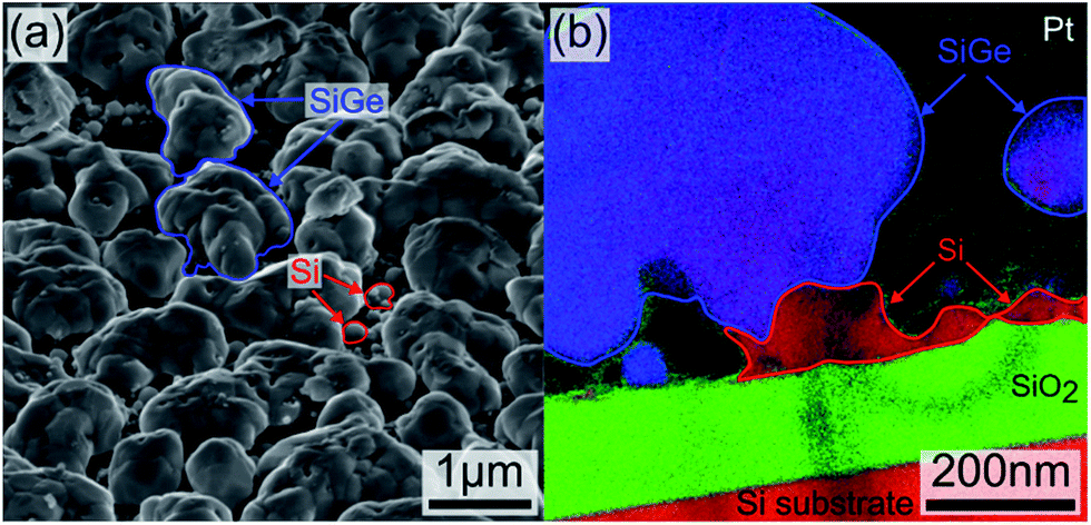
The compositions of the as-deposited sample and the annealed samples (i.e. 450 °C for 10 minutes, 450 °C for 30 minutes, 600 °C for 10 minutes and 600 °C for 30 minutes) were analyzed using Raman Spectroscopy (Witek™ alpha 300) with a 532 nm excitation line and 75 mW as energy. Each measurement represents 200 integrated spectra with an acquisition time of 1 second each. The composition and the strain were determined by measuring the Si and Ge peaks shift positions. Additionally, the lattice constant and the grain size were measured using X-ray diffraction (XRD) using X'pert-Panalytical™ system equipped with copper source (λ(Kα) = 0.154 nm). The structure and morphology of the nanocrystals were analyzed by scanning electron microscopy (SEM) (FEI™ Helios NanoLab™ 650). The operating voltage and the current were set at 5 kV and 100 pA, respectively. The total porosity was determined using threshold enhancement technique in addition to watershed segmentation method using ImageJ™ software. The roughness and the grain size were examined by atomic force microscope (AFM) recorded in tapping mode (Bruker™ Dimension Icon, cantilever characteristics: 42 N m−1, 320 kHz). High-Resolution Transmission Electron Microscope (HRTEM) was used on selected samples to screen the polycrystalline aspect of the deposited layer. Dual focused ion beam system (FEI™ Helios NanoLab™ 650) was used to fabricate TEM lamellas. A standard in situ lift out method was implemented for the purpose.24–26 Fig. 1 shows the nature and the aspect of the as-deposited sample. Fig. 1(a) is a SEM micrograph of the sample (tilt view), highlighting the presence of Si nanoparticles and sub-micro SiGe particles. Fig. 1(b) is an energy filtered TEM image (EFTEM) showing different stacks used for the sample fabrication. Si, SiO2 and the SiGe appear in red, green and blue respectively. The EFTEM confirms the discontinuity of Si nanoparticles (red) used as seeding material for the growth of the SiGe compounds (blue).
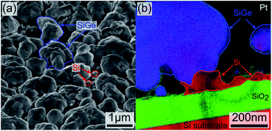 |
| | Fig. 1 (a) SEM (tilted view) and (b) EFTEM image of the deposited stack. Red, green and blue areas correspond to silicon, SiO2 and SiGe, respectively. | |
C Results and discussion
Fig. 2 shows the Raman spectra of as-deposited sample and the annealed samples considered in this study. From these spectra, four characteristic peaks are visible on all samples. The first peak measured at 521 cm−1 is related to the transversal optical phonon mode of the silicon. The remaining peaks located respectively at ≈280 cm−1, ≈400 cm−1, and ≈480 cm−1 correspond to the atomic vibrations of the Ge–Ge, Si–Ge and Si–Si bonds, respectively (transverse optic vibration modes). From these spectra, the composition of Si1−xGex compound and the strain relaxation of the layers were extracted using the Tsang's model27–29 using Si–Si and Si–Ge peaks positions according to the eqn (1) and (2):| | |
ωSi–Si = 520 − 68x − 830ε
| (1) |
| | |
ωSi–Ge = 400.5 − 14.2x − 575ε
| (2) |
where ω is the peak position, x is the Ge fraction in the grown SiGe particles, and ε is the strain parallel to the substrate (planar strain). Moreover, Vegard's law is used to predict the lattice parameter of the compound as a function of the Ge content30 as per eqn (3):| | |
aSiGe = 5.4309 + 0.20032x + 0.02674x2
| (3) |
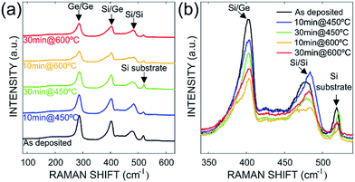 |
| | Fig. 2 (a) Full Raman spectra measured at room temperature for as deposited and annealed Si–Ge samples. (b) Raman spectra highlights and overlaps for the Si–Ge, Si substrate peaks. | |
The frequencies shifts of the Si–Si and Si–Ge modes and the different parameters extracted from eqn (1)–(3) are summarized in Table 1. We found that the Ge content of the screened samples varies between 43% and 50%. These measurements represent an average Ge composition for each samples over a surface of 1.633 μm2 (the spotsize is evaluated to 721 nm for a wavelength of 532 nm−1). This variation can be attributed to three main factors: (1) the three steps deposition with increased proportion of GeH4 in the plasma; (2) presence of heterogeneity in Si–Ge thin film along the large 6 inches Si wafer, which might occur during the layer deposition; (3) high diffusion activity of Ge atoms into the Si layer during the heat treatment. The interdiffusion can be because of high strains and concentration gradient.26,31 The effect of RTA, for instance is clearly observed on the evolution of strain as a function of annealing time and temperature. For increasing annealing temperature and dwell time, significant strain relaxation was attained in the Si–Ge layer. Table 1 gives also the calculated lattice parameters for all samples using eqn (3) taking into account the measured strain of the layer.
Table 1 Results of the composition and the strain obtained from the Raman spectra using Tsang's model27
| Sample |
ωSi–Si (cm−1) |
ωSi–Ge (cm−1) |
xGe content |
ε (%) |
aSiGe (A) |
| As-deposited |
479.6 |
403.7 |
0.51 |
0.70 |
5.58 |
| 10 min@450 °C |
483.4 |
403.1 |
0.46 |
0.68 |
5.57 |
| 30 min@450 °C |
487.9 |
404.7 |
0.43 |
0.34 |
5.54 |
| 10 min@600 °C |
483.0 |
403.3 |
0.46 |
0.66 |
5.57 |
| 30 min@600 °C |
485.9 |
406.4 |
0.48 |
0.16 |
5.54 |
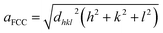
Fig. 3 depicts the XRD spectra of SiGe sub-micro particles before and after annealing at various temperatures and durations. The spectrum of as-deposited specimen shows three representative peaks of SiGe at (111), (220) and (311) located at around 27.8°, 46.2° and 54.7°, respectively. Regarding the samples annealed at 450 °C for 10 minutes and 600 °C for 30 minutes, an additional peak appears at 33° commonly known to be representative of the Si substrate on (200) diffraction.32,33 The zoom in plotted in Fig. 3 highlights the peak at around 27.8°, which is the most relevant peak emphasizing the effect of annealing on the crystallographic structure of the SiGe layer. Indeed, as it can be seen in this figure, the peak intensity is higher for annealed sample compared to the as-deposited one. This phenomenon is the result of the increase of the recrystallization rate, which occurs during the annealing process. Moreover, a peak shift is also visible and it is related to strain relaxation of the Si–Ge layer due to the change of lattice parameter as confirmed by Raman experiments. The resulting lattice parameter of the annealed samples was deduced from eqn (4) and (5) and the SiGe composition was calculated using eqn (3):
| |
 | (4) |
| |
 | (5) |
where
dhkl is the interplanar spacing,
λ is the wavelength:
λ(Kα)
Cu = 0.154 nm, and
θhkl is the Bragg's angle. In this calculation, the Ge composition of each sample is determined without considering the lattice parameter deformation due to the strain.
Table 2 gives the microstructure characteristics of all screened samples such as interplanar spacing, lattice parameter and Ge composition stoichiometry
x. Lattice parameters values calculated from (111) peak position are in good agreement with those obtained from Raman experiments (less than 1% difference). As for Raman analysis, the decrease of the Ge composition is accompanied with strain relaxation.
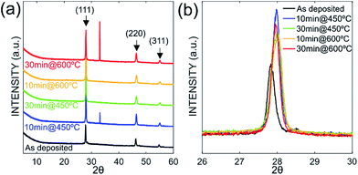 |
| | Fig. 3 XRD spectra measured at room temperature for all Si–Ge samples (a), zoom in on peak centered at around 27.8° to highlight the annealing effects (b). | |
Table 2 Results obtained from the XRD (111) spectra
| Sample |
2θ-peak position |
d111-spacing |
a-lattice parameter (Å) |
xGe content |
| As deposited |
27.831 |
3.203 |
5.548 |
0.545 |
| 10 min@450 °C |
27.951 |
3.190 |
5.524 |
0.441 |
| 30 min@450 °C |
27.950 |
3.190 |
5.525 |
0.442 |
| 10 min@600 °C |
27.980 |
3.186 |
5.519 |
0.416 |
| 30 min@600 °C |
27.933 |
3.192 |
5.528 |
0.457 |
To confirm the Ge composition measured by these non-destructive techniques (i.e. Raman spectroscopy and XRD), energy dispersive spectroscopy (EDS) analysis combined with high angle annular dark field scanning transmission electron microscope (HAADF-STEM) were conducted on two different samples: as deposited layer and annealed sample at 600 °C for 30 minutes. Fig. 4 shows the granular aspect of the two different samples. These two micrographs clearly show that the SiGe nanocrystals can be composed of different crystalline domains for both samples: as-deposited and annealed at 600 °C for 30 minutes. The different contrasts observed in the regions suggest different compositions of the SiGe compound. Elemental composition analysis is performed on these regions (delimited by clear boundaries) to determine the exact compositions of SiGe compound. The results given on the micrographs suggest three compositional domains ranging from 47.4% to 52.2%, which is in close agreement with the Ge composition extracted from Raman spectroscopy and XRD experiments. It is also worth noting the consistency of the germanium contents obtained with the three different techniques.
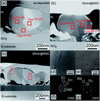 |
| | Fig. 4 TEM images of (a) as-deposited sample (b) after annealing at 600 °C for 30 minutes showing the poly crystalline aspect of the SiGe particles. EDS-STEM compositional measurements were performed on the red squares. Quantified amount of Ge for each area is shown. HAADF-STEM images at (c) low magnification of a sample annealed for 30 minutes at 600 °C. (d) and (e) are high resolution images of red squared area showing lattice structure of SiGe. (f) and (g) are fast Fourier transform of the images (d) and (e), respectively. | |
Fig. 4(c) shows a single nanoparticle observed by TEM for the sample annealed for 30 minutes at 600 °C. The image clearly shows the presence of multiple regions with various crystalline orientations. Fig. 4(d) and (e), which are high resolution zoom in of the red squared areas highlighted in Fig. 4(c), show diamond crystal structures with different zone axes that characterize the SiGe (cf. fast Fourier transform in Fig. 4(f) and (g)).
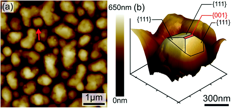
The evolution of the layer morphology as a function of annealing temperatures and durations and its impact on Si–Ge physical properties were investigated. SEM imaging for instance was used to quantify the porosity resulting from the particles clustering during the annealing process. Indeed, during the heat treatment, particles were observed to coarsen, coalesce and merge to form larger SiGe islands as shown in Fig. 5. This figure gives the microstructures of as-deposited and annealed sample at 600 °C for 30 minutes (Fig. 5(a) and 5(b) respectively). The SEM micrographs processed using threshold enhancement and watershed algorithm were used to extract the actual porosity.34 The obtained porosity is 34.9% and 19.8%, respectively for as-deposited and annealed sample at 600 °C for 30 minutes (porosity measurements for the other samples are given in Table 3). The porosity obviously decreases with increasing annealing times and durations while the grains size is increasing. Regarding the measurement of the particles size and the layers roughness AFM imaging was carried out on all samples. One example of AFM imaging is given in Fig. 6 for the as-deposited sample. Fig. 6(a) shows clearly the grains shape and the clustering effect making it easy to extract the grains size given in Table 3, whereas Fig. 6(b) emphasizes the different facets of typical nanoparticle, illustrating the high crystallinity aspect of the sample. The presence of these well-oriented facets suggests that the growth of SiGe particles is directional and monitored by a specific geometrical orientation. From Fig. 6(b), the facets seem to have a triangular shape consistent with <111> compact orientation as preferable direction of SiGe particles growth.
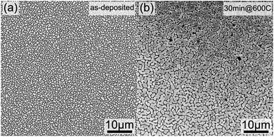 |
| | Fig. 5 SEM images of SiGe particles (a) as-deposited and (b) after 30 minutes annealing at 600 °C. | |
Table 3 Porosity, grains sizes and strain analysis for the as-deposited and annealed samples
| Sample |
Porosity (%) |
Particle size (μm2) |
Standard deviation (μm2) |
Strain ε (%) |
Stress σ (MPa) |
| As deposited |
34.939 |
0.587 |
0.481 |
0.701 |
912.702 |
| 10 min@450 °C |
23.423 |
2.612 |
2.764 |
0.682 |
210.531 |
| 30 min@450 °C |
24.734 |
2.554 |
2.082 |
0.338 |
201.604 |
| 10 min@600 °C |
22.682 |
3.264 |
2.425 |
0.660 |
374.652 |
| 30 min@600 °C |
19.791 |
4.691 |
3.573 |
0.160 |
109.076 |
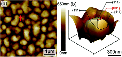 |
| | Fig. 6 AFM images (a) SiGe film appears as a cluster of nanoparticles with different shapes and sizes. (b) 3D image of one SiGe nanocrystal (red arrow in (a)) showing crystalline facets with triangular shape. | |
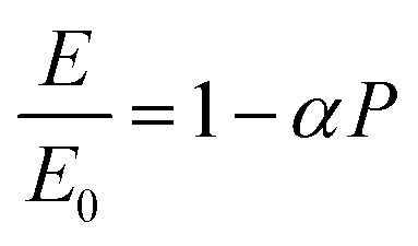
To evaluate the stress relaxation after the annealing, we followed the methodology known as law of mixture as reported elsewhere.34 This method consists of linking the mechanical properties to the degree of porosity of porous films. During the heat treatment, the material will undergo mechanical as well as crystalline property alteration35 leading to the strain relaxation caused by the relief of internal stresses inherent to fabrication process. These authors attributed this strain relaxation to the variation of apparent elastic modulus. Precisely, by plotting the ratio between the actual elastic modulus of strained sample (E) and the reference elastic modulus of the sample free of strain (E0) versus the measured porosity (P), these authors found the following relationship given in eqn (6):
| |
 | (6) |
where
α is a coefficient linked to the geometry of the porous material. Since SiGe material has a Poisson ratio close to 0.2, we used the approximation made by Rossi,
36 hence
α = 2.1. The as deposited Young's modulus was calculated using the following equation:
The stress values of the different samples are finally calculated using Hook's law:
where
ε is the strain calculated from the relationship between the Raman peaks shift.
34 Table 3 summarizes the results obtained from SEM, AFM and strain analysis, it shows that the lower porosity value (19.8%) is achieved for the sample annealed at 600 °C for 30 minutes with the highest average particle area (4.69 μm
2). This annealed sample also has the lower strain and stress values. Temperature and time both affect porosity, particles size and strain. The influence of these parameters on stress is less clear. Indeed, the sample annealed at 600 °C for 10 minutes has a higher stain value than the sample annealed at 450 °C for 10 minutes. This unexpected phenomenon is inversed for samples annealed for 30 minutes.
These results are consistent with the fact that SiGe growth is accompanied by significant strain relaxation favoring the adjustment of SiGe crystals growth along a preferred crystallographic orientation.
D Conclusions
SiGe sub-micro particles with a relatively high amount of Ge content were successfully deposited on a 200 nm silicon dioxide substrate using Si nano particles as seeding materials. The obtained compound morphology and elemental composition were investigated by various advanced characterization techniques. Specifically, Raman spectrometry was used to validate Tsang's model on polycrystalline sub-micro SiGe particles, which was subsequently confirmed by tedious techniques such as STEM-EDS and XRD. The influence of RTA parameters on the Ge stoichiometry with respect to strain relaxation was also determined. Based on this study, the following conclusions can be drawn:
• The fabricated SiGe islands are highly crystalline with an average Ge content of 40% to 55%.
• The growth of SiGe is linked to porosity and voids of interspace between the growing SiGe particles, hence grain size and strain relaxation.
• The minimum strain relaxation was found to be 0.16%, which was observed to occur after annealing at 600 °C for 30 minutes.
• The SiGe submicron particles exhibit a surface area varying, respectively from 0.59 μm2 to 4.7 μm2 for as-deposited and annealed particles at 600 °C for 30 minutes.
• After matching different observed facets of SiGe particles, these particles seem to conform to a preferred direction namely <111> while the composition stoichiometry was found unchanged. Indepth crystallography investigations are required to confirm the effective crystallographic orientation of these particles as described by Robinson et al.37
Acknowledgements
This work was carried out using state of the art Micro/Nano Fabrication, SPM/Raman and Electron Microscopy facilities at Masdar Institute of Science and technology using internal seed funds from Masdar Institute.
Notes and references
- T. P. Ernst, F. Andrieu, O. Weber, J.-M. Hartmann, C. Dupre, O. Faynot, J.-C. Barbe, J. Eymery, S. Barraud, F. Ducroquet, G. Ghibaudo and S. Deleonibus, ECS, 2006, 3, 947–961 CrossRef CAS.
- M. Amato, M. Palummo, R. Rurali and S. Ossicini, Chem. Rev., 2014, 114, 1371–1412 CrossRef CAS PubMed.
- T. Van der Donck, J. Proost, C. Rusu, K. Baert, C. Van Hoof, J.-P. Celis and A. Witvrouw, in Proc. SPIE 5342, ed. M. A. Maher and J. F. Jakubczak, 2004, p. 8 Search PubMed.
- B. Yan, L. Zhao, B. Zhao, J. Chen, G. Wang, H. Diao and W. Wang, Phys. Status Solidi A, 2012, 209, 2527–2531 CrossRef CAS.
- T. Li, J. Zhang, Y. Cao, Z. Huang, J. Ma, J. Ni and Y. Zhao, Optoelectronics letters, 2014, 10, 202–205 CrossRef.
- L. Zhang, M. d'Avezac, J.-W. Luo and A. Zunger, Nano Lett., 2012, 12, 984–991 CrossRef CAS PubMed.
- D. A. Coucheron, M. Fokine, N. Patil, D. W. Breiby, O. T. Buset, N. Healy, A. C. Peacock, T. Hawkins, M. Jones, J. Ballato and U. J. Gibson, Nat. Commun., 2016, 7, 13265 CrossRef CAS PubMed.
- L. Tsybeskov and D. J. Lockwood, Proc. IEEE, 2009, 97, 1284–1303 CrossRef CAS.
- C. G. Littlejohns, A. Z. Khokhar, D. J. Thomson, Y. Hu, L. Basset, S. A. Reynolds, G. Z. Mashanovich, G. T. Reed and F. Y. Gardes, IEEE Photonics J., 2015, 7, 1–8 CrossRef CAS.
- J. Olivares, J. Sangrador, A. Rodríguez and T. Rodríguez, J. Electrochem. Soc., 2001, 148, C685 CrossRef CAS.
- J. Qi, Y. Yang and D. He, J. Electrochem. Soc., 2008, 155, H903 CrossRef CAS.
- K. U. Joshi, D. Kabiraj, A. M. Narsale, D. K. Avasthi, T. K. Gundurao, T. N. Warang and D. C. Kothari, Surf. Coat. Technol., 2009, 203, 2497–2500 CrossRef CAS.
- K. Tao, J. Wang, R. Jia, Y. Sun, Z. Jin and X. Lin, Scr. Mater., 2015, 107, 100–102 CrossRef CAS.
- S. Joseph, N. Saraf, A. Umamaheswara, V. Madakasira and N. Bhat, Mater. Sci. Semicond. Process., 2015, 40, 655–663 CrossRef CAS.
- M. Avella, á. C. Prieto, J. Jiménez, A. Rodríguez, J. Sangrador, T. Rodríguez, M. I. Ortiz and C. Ballesteros, Mater. Sci. Eng., B, 2008, 147, 200–204 CrossRef CAS.
- T. Iwasa, T. Kaneko, I. Nakamura and M. Isomura, Phys. Status Solidi A, 2010, 207, 617–620 CrossRef CAS.
- T. Antesberger, C. Jaeger, M. Scholz and M. Stutzmann, Appl. Phys. Lett., 2007, 91, 201909 CrossRef.
- T. Sadoh, J.-H. Park, R. Aoki and M. Miyao, Thin Solid Films, 2016, 602, 3–6 CrossRef CAS.
- M. I. Ortiz, A. Rodriguez, J. Sangrador, C. Kanyinda-Malu, T. Rodriguez and C. Ballesteros, J. Phys.: Conf. Ser., 2008, 126, 12023 CrossRef.
- M. I. Ortiz, J. Sangrador, A. Rodríguez, T. Rodríguez, A. Kling, N. Franco, N. P. Barradas and C. Ballesteros, Phys. Status Solidi A, 2006, 203, 1284–1290 CrossRef CAS.
- T. Del Cano, L. F. Sanz, P. Martin, M. Avella, J. Jimenez, A. Rodriguez, J. Sangrador, T. Rodriguez, V. Torres-Costa, R. J. Martin-Palma and J. M. Martinez-Duart, J. Electrochem. Soc., 2004, 151, C326–C332 CrossRef CAS.
- M. Schoisswohl, M. Rosenbauer, J. L. Cantin, S. Lebib, H. J. von Bardeleben, J. L. Fave, J. Cernogora, G. Amato and A. Rossi, J. Appl. Phys., 1996, 79, 9301–9304 CrossRef CAS.
- J. A. Perez-Taborda, M. Muñoz Rojo, J. Maiz, N. Neophytou and M. Martin-Gonzalez, Sci. Rep., 2016, 6, 32778 CrossRef CAS PubMed.
- M. Schaffer, B. Schaffer and Q. Ramasse, Ultramicroscopy, 2012, 114, 62–71 CrossRef CAS PubMed.
- N. S. Rajput, S.-G. Kim, J. B. Chou, J. Abed, J. Viegas and M. Jouiad, MRS Adv., 2016, 1, 825–830 CrossRef CAS.
- G. Deokar, N. S. Rajput, P. Vancsó, F. Ravaux, M. Jouiad, D. Vignaud, F. Cecchet and J.-F. Colomer, Nanoscale, 2017, 9, 277–287 RSC.
- J. C. Tsang, P. M. Mooney, F. Dacol and J. O. Chu, J. Appl. Phys., 1994, 75, 8098 CrossRef CAS.
- J. Olivares, P. Martín, A. Rodríguez, J. Sangrador, J. Jiménez and T. Rodríguez, Thin Solid Films, 2000, 358, 56–61 CrossRef CAS.
- M. Mederos, S. N. M. Mestanza, I. Doi and J. A. Diniz, Thin Solid Films, 2015, 579, 116–122 CrossRef CAS.
- K. Cai, C. Li, Y. Zhang, J. Xu, H. Lai and S. Chen, Appl. Surf. Sci., 2008, 254, 5363–5366 CrossRef CAS.
- C.-Y. Wen, M. C. Reuter, D. Su, E. A. Stach and F. M. Ross, Nano Lett., 2015, 15, 1654–1659 CrossRef CAS PubMed.
- W. K. Choi, L. K. Teh, L. K. Bera, W. K. Chim, A. T. S. Wee and Y. X. Jie, J. Appl. Phys., 2002, 91, 444 CrossRef CAS.
- P. Zaumseil, J. Appl. Crystallogr., 2015, 48, 528–532 CrossRef CAS PubMed.
- A. Najar, M. Gerland and M. Jouiad, J. Appl. Phys., 2012, 111, 93513 CrossRef.
- J. H. Jang, M. S. Phen, K. Siebein, K. S. Jones and V. Craciun, Mater. Lett., 2009, 63, 289–291 CrossRef CAS.
- R. C. Rossi, J. Am. Ceram. Soc., 1968, 51, 433–440 CrossRef.
- J. T. Robinson, A. Rastelli, O. Schmidt and O. D. Dubon, Nanotechnology, 2009, 20, 085708 CrossRef PubMed.
Footnote |
| † Electronic supplementary information (ESI) available. See DOI: 10.1039/c7ra04426g |
|
| This journal is © The Royal Society of Chemistry 2017 |
Click here to see how this site uses Cookies. View our privacy policy here. 
 Open Access Article
 This Open Access Article is licensed under a Creative Commons Attribution-Non Commercial 3.0 Unported Licence
 ,
Leslie George,
Mike Tiner and
Mustapha Jouiad
,
Leslie George,
Mike Tiner and
Mustapha Jouiad