
 Open Access Article
 This Open Access Article is licensed under a
 Creative Commons Attribution 3.0 Unported Licence
Electrochemical migration of Sn and Sn solder alloys: a review
Xiankang Zhong *ab,
Longjun Chena,
Bálint Medgyesc,
Zhi Zhanga,
Shujun Gaod and
László Jakabc
*ab,
Longjun Chena,
Bálint Medgyesc,
Zhi Zhanga,
Shujun Gaod and
László Jakabc
aState Key Laboratory of Oil and Gas Reservoir Geology and Exploitation, School of Oil and Natural Gas Engineering, Southwest Petroleum University, Chengdu 610500, P. R. China. E-mail: zhongxk@yeah.net; Tel: +86-028-83032210
bMax-Planck Institut für Eisenforschung, Max-Planck Str. 1, D-40237 Düsseldorf, Germany
cDepartment of Electronics Technology, Budapest University of Technology and Economics, Budapest H-1111, Hungary
dDepartment of Chemical & Biomolecular Engineering, Ohio University, OH 45701, USA
First published on 30th May 2017
Abstract
Sn and Sn solder alloys in microelectronics are the most susceptible to suffer from electrochemical migration (ECM) which significantly compromises the reliability of electronics. This topic has attracted more and more attention from researchers since the miniaturization of electronics and the explosive increase in their usage have largely increased the risk of ECM. This article first presents an introductory overview of the ECM basic processes including electrolyte layer formation, dissolution of metal, ion transport and deposition of metal ions. Then, the article provides the major development in the field of ECM of Sn and Sn solder alloys in recent decades, including the recent advances and discoveries, current debates and significant gaps. The reactions at the anode and cathode, the mechanisms of precipitates formation and dendrites growth are summarized. The influencing factors including alloy elements (Pb, Ag, Cu, Zn, etc.), contaminants (chlorides, sulfates, flux residues, etc.) and electric field (bias voltage and spacing) on the ECM of Sn and Sn alloys are highlighted. In addition, the possible strategies such as alloy elements, inhibitor and pulsed or AC voltage for the inhibition of the ECM of Sn and Sn solder alloys have also been reviewed.
1. Introduction
The growing miniaturization of electronic systems and the explosive increase in their usage have increased the failure risk in electronics. The higher density packaging has resulted in smaller components, closer spacing, thinner metallic parts, and higher gradient of electric fields. Moreover, the electronics sometimes have to operate in humid and even polluted environment. Consequently, the electronics materials are more susceptible to failure. It is reported that even small amounts of weight loss, of the order of nanograms or less, can cause problems and ultimately lead to device failure.1Electrochemical migration (ECM) is a common reliability problem which is related to failure encountered in the electronics industry. It is defined as a process by which a metal, in contact with insulating materials and under an electrical potential, is removed ionically from its initial location and is redeposited at other location. This migration often results in lowered resistance and dielectric failure.2 ECM is fundamentally an ionic process and requires electrolyte, bias voltage and time. Therefore, ECM is totally different from solid-state electro-migration which is the mass transport of metal under dry conditions due to the momentum transfer between conducting electrons and diffusing metal atoms.3 This process is also different from the whisker growth which is induced by compressive mechanical stress in electronics.4,5
The phenomenon of ECM was first observed in the late 1940s and early 1950s. Silver migration first caused large scale problems in Post Office equipment where contact springs were silver-plated in an attempt to reduce contact resistance.2 With the growing miniaturization of electronics and the explosive increase in their usage, ECM has attracted much attention because more and more reliability problems related to ECM encountered in electronics. Extensive work has been conducted on the ECM of various electronic materials such as Cu,6–23 Ag,24–41 Sn and Sn solder alloys,42–76 as well as other metals.41,77–80
Steppan et al.2 contributed a critical review of corrosion failure mechanisms of electronic materials. The ECM of Ag, Cu and Au was reviewed in detail. However, the ECM of Sn and Sn solder alloys was not covered in their review paper. In electronics, the metallic surfaces that are directly exposed to the environment are mainly the component electrodes, solder joints, and contact/connector areas. Nowadays, hot air solder leveling (HASL) surface finishes are widely employed with Sn based solder in industrial applications.42,81 Therefore, it can be considered that large part of the exposed areas is made of Sn or Sn solder alloys.42 In this case, the ECM of Sn and Sn solder alloys is extremely important in connection with reliability of electronic devices. As mentioned above, the behaviors and mechanisms of Sn and Sn solder alloys have been extensively investigated in the recent decades.42–76 For more in depth knowledge in the future work, a critical review of the ECM of Sn and Sn solder alloys is therefore needed.
This work mainly focuses on the fundamentals of ECM, and the state-of-the-art in ECM studies of Sn and Sn solder alloys. Namely, the first objective of this paper is to introduce the fundamentals of ECM including the basic processes, characteristics and significance. The second objective is to review the recent advances and discoveries, current debates and significant gaps in the field of ECM of Sn and Sn solder alloys.
2. The fundamentals of electrochemical migration
ECM occurs when two oppositely biased and closely spaced electrodes (circuits, joints or legs of components) are connected by a continuous electrolyte layer which may be a visible electrolyte layer or an invisible adsorbed layer. Some parts of metal become ionized and begin to migrate under the applied electric field. Then, a conducting filament forms between the anode and cathode, which can lead to short circuit failure of the electronics. There are two mechanisms mainly responsible for the ECM phenomena: the formation of conducting anodic filaments and dendrite growth.82The conducting anodic filaments which usually consist of metal salts emanate from the anode to the cathode.83 Lee et al.82 used a four-layered printed circuit board with an electroplated through-a-hole to determine the ECM characteristics of eutectic Sn–Pb solder at the 85 °C/85% RH condition. As is shown in Fig. 1, it is seen that conducting anodic filaments are formed near the anode.
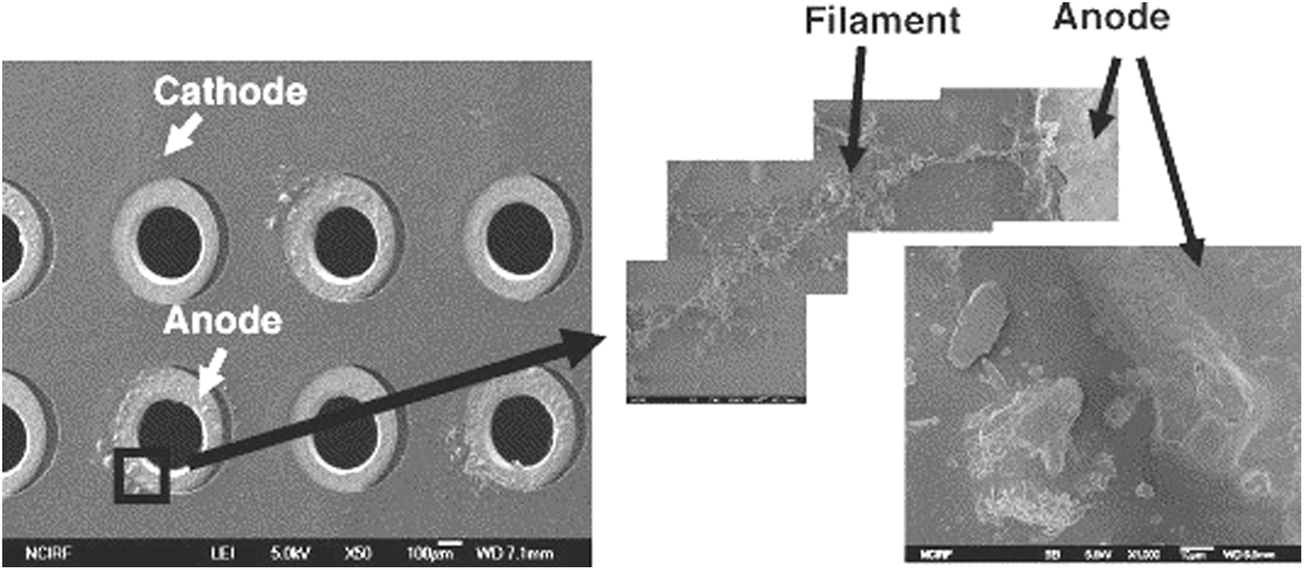 | ||
| Fig. 1 Morphology of conductive anodic filaments around the anode at through-hole-via in the PCB after 140 h at 85 °C, 85% RH. Reproduced with permission from ref. 82. Copyright 2006, Elsevier. | ||
For Sn and Sn solder alloys, most studies focus on the second ECM phenomenon: dendrite growth. Metal ions are produced at the anode and then migrate towards the cathode, where they can be reduced to metallic dendrite which then grows towards the anode. For example, the scanning electron microscopy images of Sn dendrites are shown in Fig. 2. As soon as the dendrite reaches the anode, the short circuit occurs and causes the failure of electronics.
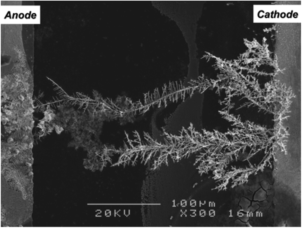 | ||
| Fig. 2 Morphology of the dendrites formed by water drop test for Sn–58Bi solder alloy in 0.001 wt% Na2SO4 at a bias voltage of 2 V. Reproduced with permission from ref. 61. Copyright 2010, Springer. | ||
Since the number of studies on dendrite growth phenomenon of Sn and Sn solder alloys are far more than conductive anodic filaments, the following introduction of the fundamentals is based the ECM phenomenon of dendrite growth. The ECM can be considered as a consecutive four-step process: (i) electrolyte layer formation, (ii) dissolution of metal, (iii) ion transport and (iv) deposition of metal ions. This four-step process is schematically shown in Fig. 3 where Fig. 3a–e indicate the sample without an electrolyte layer, the sample with an electrolyte layer, dissolution of metal, ion transport and deposition of metal ions (dendrites growth), respectively. Once the dendrite bridges the two solder joints, the shirt circuit will occur and subsequently lead to device failure.
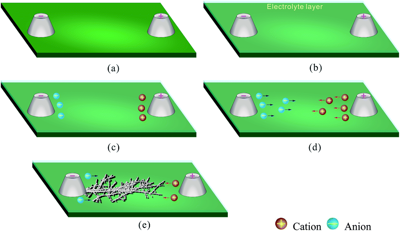 | ||
| Fig. 3 The schematic diagrams of Sn solder alloys joints (a) ECM sample, and ECM process: (b) electrolyte layer formation, (c) dissolution of metal, (d) ion transport and (e) deposition of metal ions (dendrites growth). | ||
2.1. Electrolyte layer formation
The electrolyte layer formation which is also called as path formation11,84 refers to the formation of a continuous moisture film or a condensed water layer/drop which can bridge the gaps of oppositely biased electrodes. The presence of this electrolyte layer is the precondition for the ECM to occur. Electrolyte layer formation depends upon the relative humidity, contaminant, temperature, and surface conditions of materials in electronics.To cause ECM, humidity is necessary, where a moisture layer of a few monolayers is fully sufficient. Lee et al.85 reported that a certain number of layers sufficient to start corrosion processes will be formed on metal surface at a critical humidity of about 60% to 70% at room temperature, depending on the substrate polarity and its surface energy. Moreover, hygroscopic contaminants such as chlorides apparently lower the critical humidity of adsorption. E.g., the materials which are exposed to contaminated atmospheres of relative humidity as low as 40% are still covered by electrolyte layers of a thickness of several monolayers.86,87 As the temperature changes, the relative humidity of the air also changes. If the temperature drops to below the dew point compared to the surrounding air, the relative humidity will at some point exceed 100% and a layer of water can be formed on the surface.88 When the temperature rises again, the water evaporates and the water layer becomes thinner and thinner or even totally disappears. In addition, some factors related to surface conditions including chemical constituents of fluxes applied for soldering, the composition of the board materials such as laminate and board finish, and surface roughness will also affect the formation of electrolyte layer.7 Therefore, as the precondition for the ECM to occur, the electrolyte layer formation is affected by multiple factors, making it relatively complicated.
From the corrosion electrochemistry point of view, a change in the thickness of the electrolyte layer affects a number of processes, e.g., the mass transport of dissolved oxygen, the accumulation of products, and the hydration of dissolved metal ions.89–93 Likewise, a change in thickness of the electrolyte layer will also apparently affect the ECM process. Warren et al.94 compared the ECM behaviors of Cr–Cu–Cr metallization under three types of experimental conditions including bulk solution, thin electrolyte layer and adsorbed moisture layer. It was found that dendrite morphology and dendrite growth rates were nearly identical for immersion tests in both bulk solution and thin electrolyte layer, but were quite different in adsorbed moisture layer. Zhong et al.50 investigated the ECM behavior of Sn under the electrolyte layer with different thicknesses from 30 μm to 1000 μm and found that dendrite growth rate first decreased and then increased with decreasing thickness of electrolyte layer. Apparently, the thickness of electrolyte layer is of significance in understanding the ECM mechanism.
However, until now there are two main limitations in quantitative analysis the effect of electrolyte layer thickness on ECM. On the one hand, most of the studies on ECM mechanisms were performed using water drop test or thin electrolyte layer test where the exact thickness of electrolyte layer could be known,95 however, such tests could not adequately represent failure processes which actually occur in ultra-thin layers of moisture collected from ambient air. On the other hand, the exact thickness of the moisture layer has never been unknown if the ECM test is performed using simulated environment tests such as the thermal humidity bias test where just the relative humidity and temperature are controlled.28 Actually, there are several techniques such as ellipsometry,96 sum-frequency-generation vibrational spectroscopy and scanning polarization force microscopy,97 attenuated total reflection infrared spectroscopy98 and ambient-pressure X-ray photoelectron spectroscopy99,100 that can be used to in situ measure the thickness of ultra-thin electrolyte layer, even a few monolayers of water. Therefore, it can be expected that the exact thickness of electrolyte layer in the simulated environment tests of ECM can be known in the future.
2.2. Dissolution of metal
The bias voltage applied across the closely spaced electrodes is usually in the voltage-range from a few volts up to several hundred volts in operating conditions of electronics.18,19 Therefore, the dissolution of metal will occur in the presence of a continuous electrolyte layer which bridges the anode and cathode, as described by reaction (1):| M → Mn+ + ne− | (1) |
| O2 + 2H2O + 4e− → 4OH− | (2) |
Accordingly, other ions such as OH− are also formed in electrolyte layer during the dissolution of metal.
The dissolution of metal is of utmost significance for ECM because it supplies the metal ions and other ions for the subsequent steps. To some extent, the dissolution rate can determine the whole ECM process. Takemoto et al.76 investigated ECM of Sn and Sn solder alloys in distilled water and found that large anodic dissolution rate seemed to be responsible for high ECM susceptibility. Minzari et al.42 studied the ECM of Sn under water drop with different Cl− and Br− concentrations. It was found that the ECM probability first increased and then decreased with increasing anodic dissolution rate of Sn if all parameters were held constant except Cl− and Br− concentrations in water drop. Jung et al.65 reported the dissolution of Sn at the anode was probably the rate-determining step of ECM of Sn–3.0Ag–0.5Cu solder in NaCl solution and Na2SO4 solution. Barton and Bockris101 used silver wire as an anode to investigate the dendrites growth of silver in liquid sodium nitrate and potassium nitrate. They found that for a given electrode and concentration, a critical current density existed below which no dendrites formed. This critical current density was proportional to the concentration of Ag+ which was related to the anodic dissolution of Ag. All of these studies demonstrate that dissolution of metal plays a key role in ECM and this step should significantly be taken into consideration in analysis of ECM mechanism.
2.3. Ion transport
The metal ions and other species are transported by electrical migration, diffusion and/or convection, as schematically illustrated in Fig. 4 in which the ion transport during the ECM of Sn solder alloy is taken as an example. The bias voltage applied across the two electrodes generates an electric field between cathode and anode. When an electric field is applied to ions in an electrolyte, the ions will move with the electric field. This phenomenon can be called as electrical migration. These ions migrate through the electrolyte with a characteristic velocity. The migration velocity of an ion is determined by ion mobility and the magnitude of the electric field, as is described in eqn (3),102| v = μE | (3) |
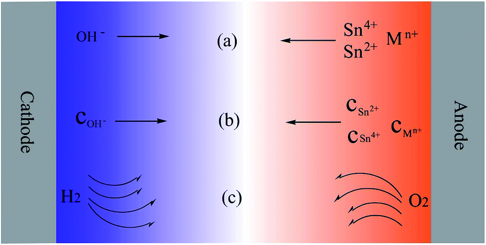 | ||
| Fig. 4 Schematic diagrams of ion transport in electrochemical migration of Sn solder alloys (a) electrical migration, (b) diffusion and (c) convection. The blue color represents the concentration distribution of OH− and the orange color represents the concentration distribution of Sn4+, Sn2+ and Mn+ (M represents alloy element in Sn solder alloys) in electrolyte layer. | ||
As the ECM proceeds, metal ions and other species are produced, resulting in the presence of concentration gradients over the distance between the cathode and anode, and consequently causing diffusion. For example, the concentrations of metal ions at the anode are much higher than that at the cathode, while the concentration of OH− at the cathode is much higher than that at the anode, as schematically illustrated in Fig. 4 in which the blue color represents the concentration distribution of OH− and the orange color represents the concentration distribution of metals in the electrolyte layer. The concentration gradients will drive the ions to move from a region of high concentration to a region of low concentration.
Convection is another way to transport the ions during the ECM process. For the corrosion under thin electrolyte layers, the convection is usually neglected, since the electrolyte is assumed stagnant and thin enough to neglect the effect of natural convection.103 However, the convection could apparently affect the ion transport during the ECM process in condensed conditions. E.g., a strong convection could be caused by the collapse of hydrogen bubbles derived from the H+ reduction at the cathode.23,42,53,104 This influence becomes more obvious if a higher bias voltage is applied between the cathode and anode. Additionally, the electro-convection may also affect the dendrites formation (deposition of metal ions) during the ECM. Fleury et al.105,106 found the space charge could create an electro-convection in the vicinity of dendrites, affecting the concentration distribution of ions, and subsequently, the deposition kinetics was changed.
2.4. Deposition of metal ions
Once the metal ions reach the cathode, the deposition will occur, as described in reaction (4).| Mn+ + ne− → M | (4) |
The shape and morphology of the electrodeposit and surface roughness strongly depend on the path of current flow and the concentrations of species involved in the electrolytic processes.107,108 The deposition of metal ions in ECM occurs under a thin electrolyte layer or a moisture electrolyte film where an uneven current distribution on the surface of electrode usually exists under such a layer or film due to the high solution resistance and the difficulties in species transport.42,109 Consequently, preferential nucleation and growth may occur at some locations of cathode, and thereby dendrites grow, as shown in Fig. 2 and 3e.
The dendrite formation consists of two consecutive stages: initiation and propagation. A critical overpotential is a necessity for the dendrite initiation. Shyu110 studied the electrodeposition of copper in CuSO4/H2SO4 solution and he reported 500 mV as the critical overpotential for copper dendrite formation. Similarly, Popov et al.111 reported a critical overpotential of 550 mV for copper dendrite formation in CuSO4/H2SO4 solution where a platinum electrode was as a cathode. For the initiation of dendrite during the ECM process in electronics, such an overpotential is usually alternatively represented by a critical bias voltage which is applied across the anode and cathode.
Meanwhile, a dendritic precursor is also needed at the beginning of the initiation stage, which will determine where the preferential nucleation to start. However, it is still not clear what a precursor is. Steppan et al.2 summarized three possibilities: a surface imperfection, a screw dislocation pyramid of the metal crystal, and a surface roughness element formed by the codeposition of foreign species. The appearance of the precursor disturbs the flow of current towards the electrode, causing the deposition rate at the peak of the precursor to be higher than that of the flat electrode surface. Consequently, a protrusion is gradually developed, where a complete characteristic of a dendrite at the end of the initiation stage can be found.
Usually, large part of the time is spent on initiation stage, rather than the propagation stage. E.g., Xia et al.73 in situ observed on the ECM of Sn–8Zn–3Bi solder joint under a water drop and found that initiation time is much longer than propagation time. Zhong et al.53 studied the ECM of Sn under 100 μm-thick electrolyte layer containing 1 mM Cl− with a bias voltage of 3 V. They found that the initiation stage took about 100 seconds while the total ECM time (from the beginning of ECM test to the time when a short circuit occurs) was 119 seconds. Minzari et al.45 reported a similar phenomenon during the ECM of Sn–37Pb solder alloy in 10 ppm NaCl solution at a bias voltage of 3 V.
During the propagation stage, a dendrite with a needle or tree-like shape has a faster growth rate at its tip than that of the rest of the electrode surface. Several reasons can be used together or separately to explain this special phenomenon. On the one hand, the electric field strength at the tip is greater than at the flat surface. This is because as the dendrite grows, the distance between the tip of dendrite and the anode is reduced, which will cause a stronger electric field at the dendrite tip, thereby making subsequent deposition of metal ions at the dendrite tip.42 On the other hand, the transport path of metal ions in the electrolyte to the tip is shorter than to the electrode surface,73 resulting in the preferential deposit at the tip of dendrite. Another possible reason is that the changes in diffusion mode when the whole ECM is predominated by the diffusion. As the tip of dendrites becomes sharp, spherical diffusion of metal ions begins to replace linear diffusion, making deposit of metal ions at the tip faster than that on the electrode surface.2
As soon as the dendrite reaches the anode, the short circuit occurs and causes the failure of electronics. The time from the beginning of ECM test to the time when a short circuit occurs is called time-to-failure61,62,65–68 or time-to-short,49–52,71–73 which is an extremely important parameter used to quantitatively assess the ECM susceptibility of materials. Some investigators also called the time-to-failure as the failure time.60 However, time-to-failure is used in this work.
In addition, it is necessary to mention that not only the metal ions could be deposited at the cathode, but the metal complex ions such as [Sn(OH)6]2− could also be reduced to metal deposit at the cathode.42,53,112
2.5. Study methods for the electrochemical migration
There are four study methods for the electrochemical migration, i.e., highly accelerated stress test (HAST), thermal humidity bias (THB) test, water drop (WD) test and thin electrolyte layer (TEL) test.In HAST, high temperatures (100–175 °C) at controlled humidity levels (50–85% RH) and bias voltage are employed as stress factors.113 The THB test is very similar to HAST, but its employed temperature is usually lower than that in HAST.47,59,70,72 Both HAST and THB test cannot only simulate the operating conditions of electronics but can also be performed in accelerating conditions in laboratory as well as industry assessment. However, it shows a poor availability in quantitative analysis because the parameters including the locations of the electrolyte layer formation and the thickness of electrolyte layer are uncertain. The WD and TEL tests are performed respectively by placing a drop of electrolyte and a thin electrolyte layer between adjacent oppositely biased joints or circuits.23,42–53,60–69 Both WD and TEL tests cannot simulate the electrolyte layer formation process, however, both methods show better in situ inspection availability than HAST and THB test. The detailed description about the advantages and disadvantages of study methods of ECM can be found elsewhere.95
3. Migration process of Sn and Sn solder alloys
Sn is susceptible to ECM,114 and worse of all that, Sn and Sn solder alloys make up a large part of the metallic materials that are directly exposed on the surface of an electronic printed circuit board assembly.43,115 Due to these reasons the ECM of Sn and Sn solder alloys is highly significant in connection with the reliability of electronics. Therefore, it has attracted researchers' more and more attention.42–76 Table 1 is a summary of ECM studies of Sn and Sn solder alloys by various investigators (note that it is impossible to list all the literature in this table.). This table enables one to compare electrode materials, the substrate materials, and the significant experimental parameters including the spacing between electrodes, applied bias voltage, and contaminants or test environments, and the test methods used in the past investigations. The migration process, the effects of alloy elements, contaminants and electric field on ECM of Sn and Sn solder alloys, as well as the inhibition of ECM of Sn and Sn solder alloys are covered in the following sections.| Materials | Substrates | Spacing (mm) | Bias voltage (V) | Electrolytes, or temperature and RH | Test methods | References |
|---|---|---|---|---|---|---|
| a Not specified.b Water drop test.c Thermal humidity bias test.d Thin electrolyte layer test.e Fiberglass reinforced epoxy (flame resistant-4).f Highly accelerated stress test. | ||||||
| Sn | Al2O3 | NSa | 3–12 | NaCl, KBr, adipic acid, dust | WDb | 42 |
| Sn–2Pb | Al2O3 | NS | 5, 12 | NaCl | WD | 43 |
| Sn | Al2O3 | NS | 5, 12 | Flux residue, deionized water | WD | 44 |
| Sn–3Pb | Al2O3 | NS | 3, 12 | NaCl | WD | 45 |
| Sn | Al2O3 | 1 | 1–25 | NaCl, flux residues | WD | 46 |
| Sn | Al2O3 | 1 | 5–10 | NaCl, 15–65 °C, 60–80% RH | THBc | 47 |
| Sn | Al2O3 | 0.91 | 5, 10 | NaCl | WD | 48 |
| Sn | Epoxy resin | 0.5 | 2–10 | NaCl, citrate ions | TELd | 49 |
| Sn | Epoxy resin | 0.5 | 3 | NaCl | TEL | 50 |
| Sn | Epoxy resin | 0.5 | 0–3 | NaCl | TEL | 51 |
| Sn | Epoxy resin | 0.5 | 3 | NaCl | TEL | 52 |
| Sn | Epoxy resin | 0.5 | 2–10 | NaCl | TEL | 53 |
| Sn | FR4e | 0.5 | 3 | NaCl | WD | 54 |
| Sn–0.3Ag–0.7Cu–0.1X, Sn–0.8Ag–0.7Cu–0.1X, (X: micro-alloys) | FR4 | 0.5 | 10 | NaCl | WD | 55 |
| Sn, Sn–3.8Cu–0.7Ag, Sn–37Pb, Sn–20Pb, Sn–37Pb, Sn–80Pb | FR4 | 0.5, 1, 1.5, 2, 2.5, 3 | 10 | Distilled water | WD | 56 and 57 |
| Sn | FR4 | 0.2 | 10 | 10 °C, 60% RH, 40 °C, 95% RH | THB | 28 |
| Sn, Sn–37Pb | FR4 | 0.2 | 10 | Distilled water | WD | 13 |
| Sn | FR4 | 0.5 | 10 | Distilled water | WD | 58 |
| Sn–60Pb, Sn | FR4 | 0.2 | 10 | 105 °C, 100% RH | HASTf | 59 |
| Sn–60Pb, Sn | FR4 | 0.2 | 10 | 40 °C, 95% RH | THB | 59 |
| Sn, Sn–64Pb, Sn–38Pb, Sn–12Pb | Si wafers | 0.3 | 2 | Deionized water | WD | 60 |
| Sn–58Bi, Sn–37Pb | Si wafers | 0.3 | 2 | NaCl, Na2SO4 | WD | 61 |
| Sn, Sn–37Pb, Sn–55Pb | Si wafers | 0.3 | 3 | NaCl, Na2SO4 | WD | 62 |
| Sn, Sn–37Pb | Si wafers | 0.3 | 3 | NaCl, Na2SO4 | WD | 63 |
| Sn | Si wafers | 0.3 | 0.5–3 | NaCl | WD | 64 |
| Sn–3Ag–0.5Cu | Si wafers | 0.3 | 3 | NaCl, Na2SO4 | WD | 65 |
| Sn | Si wafers | 0.3 | 3 | NaCl, Na2SO4 | WD | 66 |
| Sn, Sn–37Pb, Sn–55Pb | Si wafers | 0.3 | 3 | NaCl, Na2SO4 | WD | 67 |
| Sn–37Pb | Si wafers | 0.3 | 5, 10 | Deionized water | WD | 68 |
| Sn | FR4 | 1, 0.318, 0.1 | 6.5, 15 | Distilled water | WD | 69 |
| Sn–37Pb, Sn–3Ag–0.5Cu | FR4 | 1, 0.318, 0.1 | 6.5, 15 | Distilled water | WD | 70 |
| Sn–37Pb, Sn–3Ag–0.5Cu | FR4 | 1, 0.318, 0.1 | 50 | 85 °C, 85% RH | THB | 70 |
| Sn–37Pb, Sn–36Pb–2Ag, Sn–3.5Ag, Sn–3Ag–0.5Cu, Sn–3.5Ag–7.5Cu, Sn–4Ag–0.5Cu, Sn–8Zn–3Bi | FR4 | 0.5 | 3, 5, 10 | Distilled water | WD | 71 |
| Sn–4Ag–0.5Cu, Sn–3Ag–0.5Cu, Sn–37Pb, Sn–36Pb–2Ag, Sn–3Ag–0.5Cu, Sn–8Zn–3Bi, Sn–3.5Ag–0.75Cu, Sn–3.5Ag | FR4 | 0.3 | 3, 5, 10 | Distilled water | WD | 72 |
| Sn–4Ag–0.5Cu, Sn–3Ag–0.5Cu, Sn–37Pb, Sn–36Pb–2Ag, Sn–3Ag–0.5Cu, Sn–8Zn–3Bi, Sn–3.5Ag–0.75Cu, Sn–3.5Ag | FR4 | 0.1 | 10 | 85 °C, 75% RH | THB | 72 |
| Sn–4Ag–0.5Cu, Sn–37Pb, Sn–36Pb–2Ag, Sn–3Ag–0.5Cu, Sn–3.5Ag, Sn–8Zn–3Bi | FR4 | 0.15, 0.35, 0.65, 0.95 | 3, 5, 10 | Distilled water | WD | 73 |
| Sn–3Ag–0.5Cu, Sn–37Pb | FR4 | 0.32, 0.64 | 5, 40 | 65 °C, 88% RH | THB | 74 |
| Sn–0.7Cu–0.3Ag–0.03P–0.005Ni | FR4 | NS | 10 | HNO3 | WD | 75 |
| Sn–40Pb, In–48Sn, Sn–1.2Al | Glass slides | 0.5 | 0–4 | Distilled water | WD | 76 |
3.1. Reactions at the anode
For Sn and Sn solder alloys, the dissolution at the anode includes the dissolution of Sn and the dissolution of the alloy elements such as Pb, Ag, Cu, etc. The reactions related to the dissolution of Sn are given by reactions (5) and (6).42,49,51,70,71| Sn → Sn2+ + 2e− | (5) |
| Sn2+ → Sn4+ + 2e− | (6) |
Sn2+ formed by reaction (5) is stable to some extent as aqueous ion in a slightly acid solution.112 Sn4+ formed by reaction (6) co-exists with Sn2+. Additionally, the direct oxidation of Sn to Sn(OH)4 could also occur at the anode surface, which is preferred as the pH increases towards the neutral side,42 as described in reaction (7).
| Sn + 4H2O → Sn(OH)4 + 4H+ + 4e− | (7) |
Although some investigators proposed that Sn could directly reacted with OH− at the anode during the ECM to form Sn(OH)2 and/or SnO,66,75 it seems to be impossible because the solution at the anode side is acidic based on the results of in situ pH inspection as the ECM proceeds.42,43,48,49,52,53
The evolution of oxygen by water dissociation could occur at the anode surface as described by reaction (8) if the bias voltage is high enough.62,115
| 2H2O → 4H+ + O2 + 4e− | (8) |
The oxidation of some anions such as Cl− from contaminants is also possible, especially for conditions where a high bias voltage is used, as shown in reaction (9).49,53,77
| 2Cl− → Cl2 + 2e− | (9) |
Besides the electrochemical reactions mentioned above, it is also possible that an additional chemical reaction, the hydrolysis of Sn4+ occurs and forms precipitate Sn(OH)4 at the anode surface:42,49,53
| Sn4+ + 4H2O → Sn(OH)4 + 4H+ | (10) |
Based on reactions (7), (8) and (10), the local pH on the anode surface will definitely decrease. Some investigations were performed to in situ inspect the localized pH distribution during the ECM. The pH at the regions close to anode changed to acidic during the ECM.42,43,48,49,52,53 E.g., the real time visualization of localized pH distribution at the anode and cathode surface using pH indicator during the ECM test of Sn is shown in Fig. 5.53 It is seen that pH at the anode decreases over time as compared with the initial stage. Moreover, the acidic areas spread out with time (Fig. 5b–d).
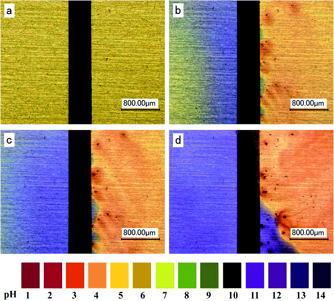 | ||
| Fig. 5 Visualization of localized pH distribution on the both electrodes using pH indicator in electrolyte layer containing 1 mM of chloride within a time interval of (a) 0 second, (b) 2 seconds, (c) 10 seconds and (d) 100 seconds (anode is on the right and cathode is on the left). Reproduced with permission from ref. 53. Copyright 2013, Elsevier. | ||
3.2. Reactions at the cathode
The reduction of O2 as described in reaction (11) and the reduction of H2O as described in reaction (12) should be involved in the cathodic reactions during the ECM.42,49,53,62,70,71,115| O2 + 2H2O + 4e− → 4OH− | (11) |
| 2H2O + 2e− → H2 + 2OH− | (12) |
The reduction of O2 consists of reduction of dissolved O2 in the electrolyte and the O2 diffused from the electrolyte/air interface. Investigation was performed to measure the cathodic polarization curves of Sn under thin electrolyte layer and found that water reduction dominated the corrosion process if the cathodic polarization potential is more negative than the potential for the water reduction.90 In electronics, the bias voltage applied across two electrodes may easily be as high as a few volts. This means the cathodic polarization potential applied at the cathode may often more negative than the potential of water reduction. Moreover, the concentration of oxygen including the dissolved oxygen and diffused oxygen is actually relatively low in the electrolyte layer. Therefore, the water reduction could be the main reaction under such conditions.
The most important cathodic reaction which is directly related to the ECM susceptibility should be the reduction of metal ions. Since Sn is usually the dominant element in the solder alloys, the reductions of Sn2+ and Sn4+ are definitely present at the cathode, as described by reactions (13) and (14).
| Sn4+ + 4e− → Sn | (13) |
| Sn2+ + 2e− → Sn | (14) |
The reduction of alloy element metal ions may also be involved during the deposition.
In addition, in strong alkaline conditions the reduction of stannic complex may be involved in the cathodic reaction. This will be further discussed in detail in dendrites growth section.
3.3. Precipitates formation
The migration of the ions such as Sn4+, Sn2+, Mn+, OH−, H+, etc. driven by electric field, diffusion and/or convection will occur after their formation. During their migration, precipitates will be formed which mainly come from three types of possible reactions. On the one hand, precipitates Sn(OH)4, Sn(OH)2 and M(OH)n will be formed when OH− meets with Sn4+, Sn2+ and Mn+ during their migration processes, respectively, as described in reactions (15)–(17).| Sn4+ + 4OH− → Sn(OH)4 | (15) |
| Sn2+ + 2OH− → Sn(OH)2 | (16) |
| Mn+ + nOH− → M(OH)n | (17) |
These precipitates can be easily formed due to very low solubility product constants, as is summarized in Table 2.116–118
On the other hand, the direct oxidation of tin to Sn(OH)4 and the hydrolysis of Sn4+ as respectively described in reactions (7) and (10) will also contribute to a part of the total amount of precipitates. The formed Sn(OH)4 and Sn(OH)2 can also be respectively dehydrated to SnO2 and SnO which are thermodynamically stable, as described by reactions (18) and (19).63,64,120,121
| Sn(OH)4 → SnO2 + 2H2O | (18) |
| Sn(OH)2 → SnO + H2O | (19) |
It should be pointed out that amphoteric Sn(OH)4 can be dissolved in acidic media as stannic ions Sn4+ (reaction (20)) and in alkaline media as [Sn(OH)6]2− (reaction (21)).122
| Sn(OH)4 + 4H+ → Sn4+ + 4H2O | (20) |
| Sn(OH)4 + 2OH− → [Sn(OH)6]2− | (21) |
At last, other precipitates such as SnCl4, AgCl and CuCl2, PbSO4 may also be formed during the ECM process,118 depending upon the composition of solder alloys and the type of contaminants in the electrolyte layer.
The formation of precipitates remarkably affects the ion transport. Firstly, the formation of precipitates will consume metal ions before they reach the cathode. Thereby the concentration distribution of metals ions will be changed. Secondly, the formation of precipitates between cathode and anode will also hinder the movement of ions, thus it may even block the metal ions from reaching the cathode.42,52,53 It is reported that the height of the formed precipitates could be measured by a 3D optical microscope.49,53 E.g., Fig. 6 shows the 3D micrograph of electrodes for the ECM of Sn under 100 μm-thick electrolyte layers containing 17 mM of chloride at bias voltage of 5 V.53 It is seen that the precipitates with a height of 162 μm are formed after 3000 s between the anode and cathode when the electrolyte layer thickness is 100 μm. Accordingly, the precipitates can act as a wall-like barrier impeding the transport of ions due to the fact that the height of the accumulated precipitates is more than the thickness of the electrolyte layer.
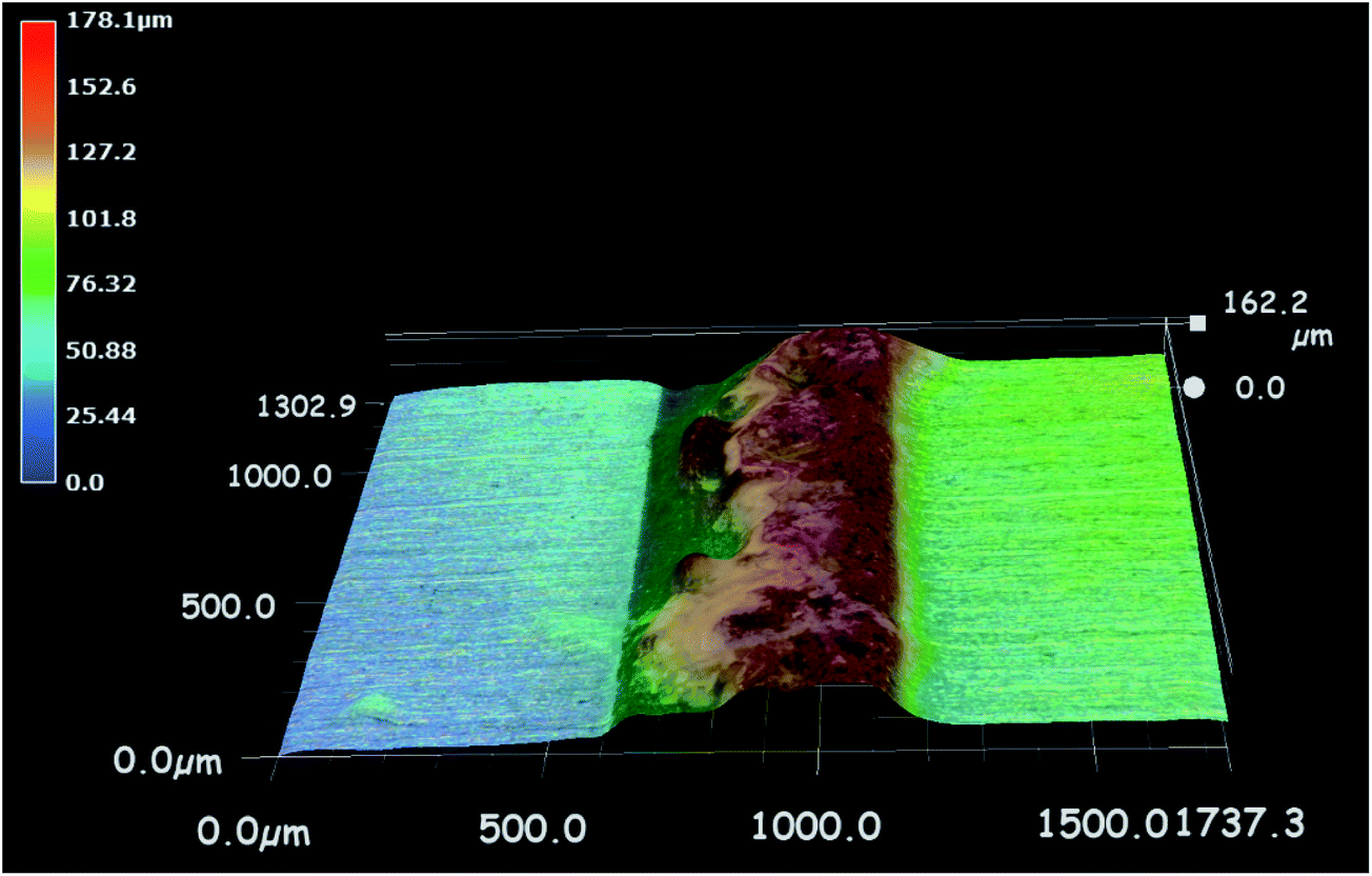 | ||
| Fig. 6 3D micrograph of precipitates formed during the ECM of tin under 100 μm-thick electrolyte layer containing 1.7 × 10⁻² M of chloride at bias voltage of 5 V. The height of the precipitates barrier is about 162 μm (anode is on the right and cathode is on the left). Reproduced with permission from ref. 53. Copyright 2013, Elsevier. | ||
3.4. Dendrites growth
The dendrites growth in ECM is essentially a kind of electrodeposition under non-uniform electric field. In acidic and weak alkaline environment, the dendrite growth of Sn and Sn solder alloys can be in general attributed to the reduction of metal ions as described in reactions (4), (13), and (14). However, in a strong alkaline environment, the reduction of some complex ions should also be taken into consideration. E.g., [Sn(OH)6]2− can be easily formed through reaction (21). As already mentioned above, [Sn(OH)6]2− can be reduced to metallic Sn, which is widely accepted in alkaline plating of tin,42,53,112 as is described in reaction (22).| [Sn(OH)6]2− + 4e− → Sn + 6OH− | (22) |
Although it will be repelled by the cathode since [Sn(OH)6]2− is inherently negatively charged, here the movement of [Sn(OH)6]2− to reach the cathode could be driven by diffusion and/or convection.43,53,112
As soon as the dendrite reaches the anode, the short circuit occurs and causes the failure of electronics. The morphologies of dendrites of Sn and Sn solder alloys vary from needle-like, tree-like and powder-like, which strongly depend on the path of current flow and the concentrations of species involved in the electrolytic process.107,108 It is interesting that Dominkovics and Harsányi56,57 reported that a fractal description of the morphology could be used to analyze the dendrites growth of Sn and Sn solder alloys. Most importantly, the fractal dimensions of dendrites formed during ECM could be used in failure analysis in “first and fast” identification of critical metallic elements without the application of chemical micro-analytical methods.
4. Effect of alloy elements
4.1. Pb
With a melting temperature of 183 °C, the eutectic Sn–Pb solder alloys allow soldering conditions that are compatible with most substrate materials and devices.123,124 As one of the primary components of eutectic solders, Pb provides many technical advantages such as (i) reduces the surface tension of pure tin,125 (ii) prevents the transformation of white tin to gray tin,126 and (iii) serves as a solvent metal.124 Therefore, Sn–Pb solder alloys were widely used in electronics industry. Although the restriction of hazardous substances (RoHS) effectively bans the use of Pb in electrical products, there is still exemption for some special Sn–Pb solders such as high-Pb solders (contain 85% by weight or more Pb) which are broadly used in automotive, space, oil and gas, and avionics industries.127,128 So the ECM of Sn–Pb solder alloys still deserves further study.The ECM behaviors of Sn–Pb alloys with different Pb contents are strongly related to the migration environment. According to the literature, three main environments were used including pure water or distilled water,78,81 chloride-containing solution60–64,67,68 and sulfate-containing containing solution.61–63,67 It can be summarized that the time-to-failure which is proportional to the ECM resistance of Sn–Pb solder alloys decreases with increasing Pb content in a pure water or chloride-containing solution, whereas it increases with increasing Pb content in sulfate-containing solution. A few examples are given below.
Yu et al.71 compared the ECM behaviors between Sn–37Pb solder alloy and Sn–36Pb–2Ag solder alloy in distilled water. They concluded that the main migration element was Pb. Takemoto et al.76 reported that in pure water pure Pb showed the highest susceptibility of ECM, thereby the addition of Pb increased the susceptibility, and Sn had the lowest susceptibility compared to that of Pb and Sn–40Pb solder alloy. Lee et al.82 investigated the ECM characteristic of Sn–Pb solder alloys with varying DC bias voltages under 85 °C and 85% RH condition. They found that Pb was more susceptible to ECM failure than Sn in the eutectic Sn–Pb solder alloys.
The ECM phenomenon of Sn–Pb solder alloys containing different Pb contents in chloride-containing solution is similar to that in pure water. Lee et al.60,63,64 studied time-to-failure of the pure Sn, Pb and Sn–Pb solder alloys in 0.001 wt% NaCl solution using water drop test. The representative results were shown in Fig. 7.60 It was found that the time-to-failure increased with decreasing Pb content, and pure Pb showed the shortest time-to-failure. This was ascribed to that a passive layer on Sn surface could be formed in NaCl solution, but not for Pb. Yoo et al.62,67 also found that the time-to-failure of Sn–Pb solder alloys decreased with increasing Pb content in chloride-containing solution.
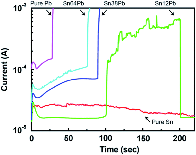 | ||
| Fig. 7 In situ current–time relationship and insulation failure during water drop test while applying 2 V in 0.001 wt% NaCl solution at room temperature with respect to alloy composition of Sn–Pb solders. Reproduced with permission from ref. 60. Copyright 2011, Springer. | ||
Lee et al. and Yoo et al.60–62,67 performed respectively a series of ECM experiments of Pb, Sn and Sn–Pb solder alloys in sulfate-containing solution. They found that the time-to-failure increased with increasing Pb content, indicating that the addition of Pb increased the ECM resistance of Sn–Pb solder alloys in sulfate-containing solution. This is a reverse phenomenon in contrast to that in chloride-containing solution and pure water. It was believed that Pb was protected from corrosion attack in sulfate by forming an insoluble layer of PbSO4 or PbO.63 The extremely low solubility of PbSO4 (see Table 2) and the insoluble property of PbO are favorable for the formation of an insoluble layer on the solder alloys surface.
4.2. Ag
Sn–Ag solder alloys have been considered strong candidates to replace the Sn–Pb solder alloys because of two main reasons. On the one hand, their properties are reasonably compatible with those of the Sn–Pb solder alloys,129,130 and on the other hand, they have better mechanical properties (ductility, creep resistance and thermal resistance) than the Sn–Pb solder alloys.131 The eutectic composition for the Sn–Ag binary system occurs at Sn–3.5Ag. The eutectic temperature is 221 °C.The addition of Ag into Sn matrix can form a chemical stable intermetallic compound Ag3Sn, in which Ag is difficult to escape during the ECM, resulting in that Ag migration is prevented. Therefore, it is generally considered that the migration characteristics of Sn–Ag solder alloys are still related to the dissolution characteristics of Sn,27,65,71,132 although that pure Ag is one of the most susceptible metals to ECM.24
Yoo et al.27 evaluated the ECM susceptibility of Sn, Sn–3.5Ag and Sn–3Ag–0.5Cu solder alloys in 0.001 wt% Na2SO4 at room temperature. They found that Ag addition increased the time-to-failure of solder alloys and the dendrite was mainly composed of Sn regardless of the solder alloys. It was attributed to that the addition of Ag improved the passivation behavior and pitting corrosion resistance and formed inert intermetallic compounds, thus, the dissolution of Ag was suppressed and only Sn was dissolved. Tanaka et al.132 also reported that in Sn–3.5Ag solder alloys, Ag combines with Sn to form a stable compound Ag3Sn that did not dissolve during ECM, and therefore the migration resistance of Sn–Ag solder alloys was related to the dissolution characteristics of Sn. Yu et al.71 found that the main element was Pb for the ECM of Sn–37Pb and Sn–36Pb–2Ag solder alloys in distilled water. While for Sn–Ag and Sn–Ag–Cu solder alloys, Sn led the migration. Similarly, He et al.74 also reported that in the ECM of Sn–3Ag–0.5Cu solder alloy, Sn always dominated composition of dendrites and Ag migrated only occasionally. Jung et al.65 even thought that Ag did not take part in ECM of Sn–3Ag–0.5Cu in NaCl and Na2SO4, and they believed that Sn was the only element that contributed to ECM of Sn–3Ag–0.5Cu solder alloy. These results demonstrate that the ECM of Sn–Ag solder alloys is still determined by Sn, but not Ag. Additionally, Medgyes et al.133 found that Sn–0.8Ag–0.7Cu solder alloy had a lower resistance against ECM than Sn–0.3Ag–0.7Cu. This was attributed to that Sn–0.8Ag–0.7Cu solder alloy had a significantly higher corrosion rate than the Sn–0.3Ag–0.7Cu, since the formed inhomogeneous SnOx was located significantly deeper in case of Sn–0.8Ag–0.7Cu.
4.3. Cu
Sn–Cu solder alloy is also one of the available alternatives of Sn–Pb solder alloy. The Sn–Cu binary alloy has a eutectic composition of Sn–0.7Cu with a melting temperature of 227 °C.114 As the addition of Ag into Sn, the addition of Cu into Sn matrix causes the formation of an intermetallic compound Sn6Cu5 which is also chemical stable.27 Therefore, the effect of Cu addition on the ECM of Sn solder alloys is very similar to Ag addition.Yoo et al.27 reported that Cu could improve the passivation behavior and pitting corrosion resistance of Sn based solder alloys. Most importantly, the dissolution of Cu during the ECM was suppressed because of the formation of the inert intermetallic compounds Sn6Cu5. He et al.74 evaluated the ECM behavior of Sn–3Ag–0.5Cu solder alloy under a condition of 88% relative humidity at 65 °C. They found that in the dendrites, Sn was dominated and Cu was a minor constituent. Yu et al.71 studied the ECM of a series of Sn–Ag–Cu solder alloys in distilled water using water drop test. They found Sn led the migration and Cu had a small susceptibility due to the formation of intermetallic compounds in alloys. All these studies indicate that Cu addition can improve the ECM resistance of Sn solder alloys to some extent. However, it is worthy to note that pure Cu may take part in the ECM of Sn solder alloys if a Cu substrate is used in the ECM test. This is due to that the poor wettability of solder paste leads to part exposure of Cu substrate at the wetting brim.72
4.4. Zn
The Sn–Zn solder alloy also appears to be an attractive alternative for Sn–Pb solder alloys. Sn–9Zn is the eutectic composition for the Sn–Zn system, with a melting temperature of 198 °C that is relatively close to eutectic Sn–Pb alloys.124 A few studies have been conducted on ECM of Sn–Zn solder alloys. However, there are still some inconsistencies among these ref. 72, 132 and 134 regarding the role of Zn in ECM of Sn–Zn alloys.Yu et al.72 investigated the ECM of Sn–8Zn–3Bi solder alloy in distilled water using water drop test. They found that it was always Zn to migrate, which means the alloying with Zn in solder alloy has a higher susceptibility to ECM. Hua et al.134 compared the ECM behavior of Sn–35Bi–1Ag solder alloy with and without Zn doping at 80 °C and 85% RH. It was found that Zn doping reduced the time-to-failure from 240 hours to 100 hours, indicating that Zn addition decreased the ECM resistance of Sn solder alloy. However, Tanaka132 reported that in the ECM of Sn–9Zn solder alloy, Sn still dominated the migration process, because Zn and Sn formed a passive film that suppressed the dissolution of Zn. Therefore, a further and systematic work regarding the effect of Zn addition on Sn–Zn solder alloys is needed.
4.5. Other elements
Other elements such as Bi, In and Sb could also be added into Sn matrix to form some specific solder alloys. E.g., due to the substantially lower melting temperature and a much lower tendency to scavenge gold, compared to Sn–Pb solder alloys, Sn–In solder alloys have been used for surface mounting technology applications.124 However, studies on ECM of these solder alloys are very limited. Three examples are given below.Tanaka132 found that Sn–58Bi solder alloy revealed sections of segregated Bi surface remaining and selective dissolution of Sn during the migration test. It was therefore assumed that Sn–Bi solder alloy suppressed anodic dissolution more than such materials as Sn alone or Sn-3.5Ag solder alloy. Takemoto et al.76 investigated the pure In and In–48Sn in distilled water. It was found that pure In and In–48Sn solder alloys were immune to ECM in pure water. Medgyes et al.55 used the transmission electron microscopy to detect the composition of dendrites which were formed during the ECM of Sn solder alloys with a low level of Ag. Sb was found in the dendrites, indicating that Sb also took part in the ECM of solder alloy process.
5. Effect of contaminants
Surface contaminants, especially hygroscopic types have a significant influence on the overall ECM process. The effects of contaminants on the ECM of Sn and Sn solder alloys have been extensively investigated in various research works where contaminants such as chlorides, sulfates and flux residues are mainly involved.5.1. Chlorides
Many studies about contaminants in ECM of Sn and Sn solder alloys focused on the chlorides since chloride is a common contaminant on device surfaces coming from environment. Chlorides in electronic devices may be originated from human sweat and fingerprints, dust in the air, the flux residues from the manufacturing process, the degradation of package, and even the salt spray from the seas.77 For the automotive electronics the chlorides is also easily originated from the deicing agents on the roadway.135 Chlorides have a rather complicated effect on the ECM of Sn and Sn solder alloys, because they significantly affect every step of ECM of Sn and Sn solder alloys.Chlorides can accelerate the electrolyte layer formation because of their hygroscopic properties. As already mentioned above, the electrolyte layer formation depends on the critical relative humidity, above which the condensation starts to take place. The critical relative humidity corresponds to the equilibrium relative humidity above the saturated salt solutions.77 The presence of chlorides can apparently decrease the equilibrium relative humidity. For example, Greenspan136 reported that at 25 °C, the equilibrium relative humidity is about 84% for KCl, 75% for NaCl, 33% for MgCl2 and only 11% for LiCl. Therefore, the electrolyte layer formation with the chlorides on the sample surface will be much more easily than that in the absence of chlorides.
The anodic dissolution of Sn and Sn solder alloys is also significantly affected by chlorides. On the one hand, the presence of chlorides definitely increases the conductivity of the electrolyte formed by condensation. Thus they increase the overall speed of the ECM process where the anodic dissolution is first involved. On the other hand, chloride ions are oxidized on the surface of the anode during the ECM and they leave the electrolyte forming Cl2 gas,53 but they may also form chlorine oxide and/or chlorous acid destroying the existing oxide film on the anode surface or inhibiting its formation which prevents the anode to have a passive film on the surface.77 Consequently, the anodic dissolution of Sn and Sn solder alloys is speeded.
More precipitates could be formed during the ECM of Sn and Sn solder alloys in the presence chlorides. According to reactions at the electrodes, in the presence of chlorides more amounts of metal ions and hydroxyl ions will be formed than that in the absence of chlorides, because both the anodic and cathodic reaction rates are increased. Therefore, more hydroxide such as Sn(OH4) and/or oxides precipitates such as SnO2 can be formed during the ion migration. Additionally, chloride ions can also form precipitates with metal ions, for example AgCl, CuCl2, etc.118
The increasing amount of precipitates due to the presence of chlorides will not only hinder the ion migration, but also act against the dendrite growth because the fewer metal ions can reach the cathode to be deposited. Minzari et al.42 studied the ECM of Sn using the water drop test with sodium chloride concentration up to 1000 ppm. They found that the probability of dendrite growth decreased when the chloride concentration was beyond a certain level. Furthermore, no dendrite was observed when the chloride concentration reached to 1000 ppm. Verdingovas et al.46 reported that the ECM probability of Sn in sodium chloride solution had a peak value and the migration probability tended to decrease with increase in concentration above this peak value. Zhong et al.52 studied the ECM of Sn under thin electrolyte layers with different chloride concentrations (see Fig. 8).
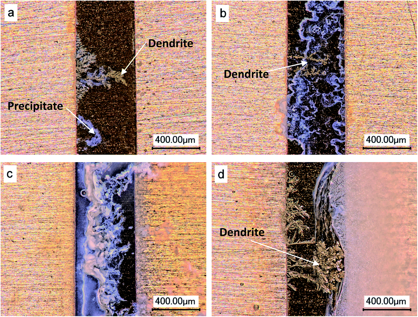 | ||
| Fig. 8 Optical micrographs of ECM of tin under 100 μm electrolyte layer with various chloride concentrations at 3 V of bias: (a) 0.1 mM, (b) 5 mM, (c) 10 mM and (d) 500 mM (anode is on the right and cathode is on the left). Reproduced with permission from ref. 52. Copyright 2013, Elsevier. | ||
It was found that in low chloride concentration, dendrite co-existed with precipitates. In intermediate chloride concentration, there were only precipitates but no dendrite because the precipitates acted as a spatial barrier, hindering the ions migration and against the dendrite growth. In high chloride concentration, the higher OH− concentration presented, resulting in the dissolution of Sn(OH)4 to form [Sn(OH)6]2−. Then, the dendrite grew again by the reduction of [Sn(OH)6]2−. In addition, the chloride ions concentration also affects the degree of uniformity of the electric field on the surface of electrode. High concentration of chloride ions in general increases the degree of uniformity of the electric field. Thus, it was found that a continuous process of deposition on the whole surface of cathode replaced the dendritic growth process at high Cl− concentrations.53,77
5.2. Sulfates
Sulfates are also one of the contaminants coming from environment. Like the chlorides, sulfates can also decrease the critical relative humidity and thereby accelerate the electrolyte formation. Moreover, the conductivity of the electrolyte and the initial reaction rate during the ECM of Sn and Sn solder alloys also increase in the presence of sulfates. The effect of sulfates on the ECM of Sn and Sn solder alloys are mainly determined by the passive film or oxide film formed on the sample in Na2SO4 containing electrolyte.61–63,66,67The presence of sulfates can affect the ability of protective film formed on Sn and Sn solder alloys. The presence of sulfates can increase stability of surface oxide film on Sn–Pb solder alloys because of the formation of a protective PbSO4 and Pb oxides film. The time-to-failure of Sn–Pb solder alloys increased with increasing Pb content.67 However, Jung et al.66 found that the time-to-failure of Sn in NaCl solution was longer than that in Na2SO4 solution. Moreover, the pitting potential of Sn in NaCl solution was also higher than that in Na2SO4 solution. They explained that this was attributed to that passive film formed on pure Sn during the water drop tests in NaCl solution was more stable than that formed in Na2SO4 solution. A similar phenomenon was also found for Sn–3Ag–0.5Cu solder alloy in Na2SO4 solution where the passive film is thinner than that formed in NaCl solution.66
5.3. Flux residues
Flux residues are usually corrosive and favorable for some steps of ECM because they are usually composed of ionic substances44,46,137–146 and other species. The most common ionic substances in flux residues are weak organic acids, or halogenides such as chlorides. Both of them will not only promote the condensation process due to their hygroscopic property, but also increase the conductivity of a condensed water layer.One or more of the short-chain weak organic acids such as adipic acid, glutaric acid, succinic acid, malic acid or formic acid are often contained in the flux residues when a no-clean flux is used.44 It is well known that a short-chain weak organic acid dissolved into the water can be partially dissociated to ionic species which result in an increase in conductivity of electrolyte layer and a decrease in solution pH. Furthermore, weak organic acids also show hygroscopic properties, although different acids have different hygroscopic properties.138,145 It was generally considered that high concentration of weak organic acids can suppress the ECM of Sn and Sn solder alloys. However, small inconsistencies in the explanation of mechanisms still exist. A few examples are given below.
Minzari et al.42 studied the effect of adipic acid on the ECM of Sn under water drop where the adipic acid concentration was ranged from 1 ppm (by weight) to saturated condition. It was found that the probability of Sn migration decreased with increasing adipic acid concentration. This effect was attributed to two factors. On the one hand, the presence of adipic acid with a significant amount could act as acidic buffer which was more suitable for precipitation formation rather than dendrite growth. On the other hand, this effect was related to the passivation of anode surface caused by organic compounds, so that anodic dissolution was decreased.
Verdingovas et al.46 investigated the ECM of Sn in flux residues using the water drop test. The flux residues came from the no-clean organic acid based wave solder flux where adipic was used as activator and synthetic resin was used as the film former. They found that there was a peak value of ECM probability at a critical concentration of flux residues (at 92 μg cm−2) and the probability of migration was reduced at both below and above this critical concentration. It was considered that at low concentration the behavior was assumed to be due to the low dissolution of metal ions, while at high concentration the effect was due to over production of metal ions thereby precipitation of tin hydroxide dominated.
Ambat et al.44 studied the effect of flux residue formed at room temperature and at 235 °C using water drop test. The main organic acid in this flux residue was also adipic acid. They found that among the samples with the flux residue formed under both conditions, only one of them showed the migration, while others did not although strong electrochemical reactions such as gas evolution was evident at the electrode at least initially. It was attributed to that acid component might be acting as an anodic inhibitor reducing the metal dissolution and thereby the dendrite growth was stopped.
Zhan et al.84 compared the ECM behaviors of Sn–37Pb with rosin-based flux and with aqueous-based flux. It was found that residues of rosin-based flux contained about 50 wt% higher concentration of weak organic acids than aqueous-based flux after reflow. This led to higher activity and promoted moisture adsorption, further reducing the time-to-failure due to the reduction of surface insulation resistance.
Tanaka et al.144 investigated the effect of flux residue on the ECM of Pb-free solder alloys including Sn–3.5Ag, Sn–9Zn, Sn–5Bi, Sn–0.8Cu and Sn–37Pb solder alloys. The samples were first solder-plated, then coated with flux, and finally heat-treated using reflow processing conditions. The flux consisted of 10 wt% rosin and 0.01 wt% activator (halogen and organic acids, the exact concentration was unknown). It was found that the presence of flux residue suppressed anodic dissolution and effectively prevented the occurrence of migration. However, with Sn–9Zn, the flux components such as halogen and organic acids could react with Zn and form a new compound layer between flux and substrate. This compound layer decreased the adhesion between flux film and substrate, subsequently, speeded the migration.
The effect of chlorides in flux residues on ECM of Sn and Sn solder alloys can be seen in chlorides section. In addition, a resin component is often contained in the flux residues. This component can easily attract dust during operation, which will eventually make surfaces hydrophilic and thus become a potential source for ions.137
5.4. Other contaminants
Other contaminants such as bromide ion,42 dust,42,44 and H2S147 have also been investigated in the ECM of Sn or Sn solder alloys.A tendency of ECM in bromide is similar to the chloride, where higher concentration of bromide reduces the dendrite formation probability.42 The component and amount of dust depend on where the dust was collected. Different ECM behaviors may be present when the dust is collected from different environments. For example, Minzari et al.42 compared the effects on ECM of Sn which was exposed in a mild dust and an aggressive dust for two months, respectively. The mild dust was collected indoor in household and the aggressive dust was collected in a pig farm. It was found that only the presence of mild dust at low levels resulted in ECM. Zou et al.147 studied the ECM of Sn–37Pb solder alloy in trace amount (1 ppm) of H2S condition at 20 °C and 40% RH. It was found that ECM occurred and the trace amount of H2S reacted easily with Pb to form PbS.
6. Effect of electric field
Once a bias voltage is applied across two oppositely electrodes, an electric field is generated between the two electrodes. The magnitude of electric field is a function of the bias voltage applied across the electrodes and the distance between the two electrodes, as described in eqn (23),
 | (23) |
6.1. Bias voltage
A bias voltage must be applied across the two electrodes for ECM to occur. The dissolution of metal, ion transport caused by electric field and the reduction of metal ions are greatly affected by the bias voltage.It has been suggested that there is a bias voltage range, outside which ECM will not occur.148 The minimum bias voltage for ECM to occur is determined by the critical potential which is required for dissolution of metal or reduction of metal ions to occur.110,111,149 The upper limit of voltage range exists. Above this voltage the failure mechanism of circuits tends to change from ECM to other failures, such as dielectric breakdown.150
Normally, the higher voltage is in this range, the shorter the time-to-failure is if the spacing between the two electrodes is fixed.3,64,69,71,148 This is because higher voltage enhances the dissolution of metal at anode and the reduction of metal ions at cathode, at the same time, accelerates migration speed of ions, resulting in rapid dendrite growth.64 However, some specific points need to be paid attention as well. E.g., at the same spacing higher bias voltage leads to faster reaction rates. In this case, more precipitation such as tin hydroxides which are formed during the migration process will hinder the ion transport and dendrite growth,53 while heavy gas evolution at the anode and cathode may also inhibit or even destroy the growth of dendrites.2,46,53 This is why under some conditions, as the bias voltage increases the probability of ECM decreases, or the time-to-failure increases.
6.2. The type of bias voltage
Three types of bias voltage including DC voltage, pulsed voltage and AC voltage have been employed in the ECM study. Most of the studies focused on ECM under DC voltage,6–47,52–76 however, relatively low attention has been drawn onto ECM under AC voltage and pulsed voltage,48,51,151–153 although they are also common voltage signals used in the electronics.The ECM of Sn and Sn solder alloys under DC voltage has been reviewed in detail in above section. The ECM of Sn and Sn solder alloys under pulsed voltage or AC voltage would be apparently different from that under DC voltage, since some processes may be introduced under pulsed and AC voltage, such as the changes in the direction of electric field, and the frequent charging and discharging processes of electrical double layer capacitance.51
Until now, only three publications related to the ECM of Sn and Sn alloy under AC voltage or pulsed voltage can be found.48,51,154 Verdingovas et al.48 studied the ECM of Sn under pulsed voltage using water drop test. It was found that varying of pulse width at a fixed duty cycle had a minor effect under investigated conditions, whereas increasing duty cycle significantly reduces the time-to-failure due to the dendrite formation and increases the charge transferred between the electrodes over time. Zhong et al.51,154 investigated the ECM of Sn under unipolar and bipolar square waves using thin electrolyte layer method. Under the unipolar square wave, it was found that at a fixed time period the rate of dendrite growth rate increases with the increasing duty cycle. While for the fixed duty cycle, the prolongation of time period was favorable for the precipitates formation and/or dendrites growth.51 For the bipolar square wave, the switch between the voltage and its reverse voltage results in a periodic switch between cathodic polarization and anodic polarization applied on the same electrode surface, periodic changes in the migration direction of ions and a circulation between dendrite growth and its re-dissolution.154
6.3. Spacing
Spacing refers to the distance between two oppositely charged electrodes. The spacing mainly affects the time of electrolyte layer formation and the time of ion transport. The longer time is needed for the continuous electrolyte layer formation and ion transport at longer spacing.84 Therefore, it is generally considered that the time-to-failure decreases with decreasing spacing at the same bias voltage.7. Inhibition of ECM of Sn and Sn solder alloys
The inhibition of ECM of Sn and Sn solder alloys is extremely significant for the improvement of reliability of electronics, however, only a few publications have specifically focused on it.49,155,156 According to the ECM mechanisms of Sn and Sn solder alloys and the previous studies regarding the ECM and its inhibition of other materials,15,152–161 the possible strategies to inhibit the ECM of Sn and Sn solder alloys are summarized, including adding alloy elements, inhibitor, and pulsed or AC voltage.7.1. Alloy elements
The addition of alloy elements can effectively decrease the ECM susceptibility of Sn solder alloys. However, it is worthy to note that the inhibition efficiency strongly depends on operating environment. Takemoto et al.76 reported that In–48Sn and Sn–1.2Al solder alloys were immune to ECM in pure water. Thus these alloys are candidates for ECM resistant solder alloys for practical use. Yu et al.71 compared the time-to-failure between Pb-free solder alloys (Sn–Ag and Sn–Ag–Cu) and Pb bearing solder alloys (Sn–37Pb and Sn–36Pb–2Ag) in distilled water. It was found that Pb bearing solder alloys have smaller time-to-failure than Pb-free solder alloy, indicating that Pb-free solder alloys exhibit lower ECM susceptibility in distilled water. Yoo et al.62 compared the time-to-failure of pure Sn, Sn–37Pb and Sn–55Pb solder alloys in 0.001 wt% Na2SO4 solution using water drop. They found that the time-to-failure increased with increasing Pb content. Therefore, it can be considered that the addition of Pb into solders could improve the ECM resistance of Sn based solder alloys in the Na2SO4 solution. As mentioned above, sulfate-containing environment is favorable for a protective film formation on the Sn–Pb solder alloys. This protective film can hinder the dissolution of Sn solder alloys and thereby inhibit the ECM development of Sn–Pb solder alloys.7.2. Inhibitor
Inhibitor is another effective way to improve the ECM resistance of Sn and Sn solder alloys. Liao et al. found that citrate ions,49 cetyltrimethylammonium bromide (CTAB)155 and Na2S156 can effectively inhibit the ECM of tin. Citrate ions could be used to inhibit ECM of Sn in thin electrolyte layer containing Cl− under a certain voltage range. On the one hand, the formation of tin–citrate complex species (negatively charged) prevented the migration of tin ions from anode to cathode. On the other hand, the presence of citrate greatly improved the passive ability of Sn in Cl−-containing solution. According to results of the measurements for the exact potential applied on electrode, the potential applied on anode is located in the passive region (see Fig. 9), thereby decreasing the anodic dissolution.49 Consequently, the ECM of Sn was effectively inhibited in a certain bias voltage range. The CTA+ in CTAB is mainly responsible for the inhibition of ECM through the selective adsorption on the Sn surface.155 The inhibition mechanism of Na2S on ECM of Sn is mainly attributed to the precipitates formation between the anode and cathode. These precipitates acted as a wall-like barrier to hinder the ions transport, which slows ECM rate or even stop ECM of tin.156 Ambat et al.44 reported that the organic acids in the flux residue can some time act as inhibitors to reduce the migration of Sn, however the exact effect depended on combination of factors such as amount, morphology, and presence of other ions such as chlorides. Therefore, according to the analysis of the formation of precipitates in precipitates section, it can also be expected that if chemicals can cause Sn or alloy elements to form precipitates between anode and cathode or at the electrode surface, they can be used to inhibit the ECM of Sn and Sn solder alloys.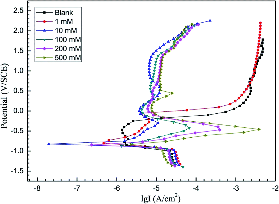 | ||
| Fig. 9 Polarization curves for tin in solutions containing 1 mM Cl− and various citrate ion concentrations (0, 1, 10, 100, 200, 500 mM). Reproduced with permission from ref. 49. Copyright 2016, Elsevier. | ||
7.3. Pulsed or AC voltage
Investigations have indicated that a pulsed voltage can suppress the dendrite growth of Sn under some conditions.48,51 Verdingovas et al.48 found that there was a suppression effect of decreasing duty cycle on dendrite formation of Sn as it reduced the rate of the dendrite formation. Zhong et al.51 reported that no dendrite growth of Sn could be seen when the duty cycle was equal to 0.1 at the periods from 10 ms to 1000 ms. These results indicate that ECM of Sn solders can be inhibited by adjusting the parameters of voltage. Similarly, it is also known that pulsed voltage can effectively suppress the Li dendrites growth in Li–metal batteries.157,158It is also reported that AC voltage can suppress the ECM development. Chaikin et al.151 demonstrated that, when an alternating 60 Hz voltage was applied between the circuits, far less ECM of Ag was produced, and no ECM of Ag could be detected at higher frequencies. Therefore, the AC could also be expected to inhibit the ECM of Sn and Sn solder alloys. Zhong et al.154 also found that the dendrite growth of Sn under bipolar square wave voltage (like AC voltage) was strongly dependent upon the semi-cycle of bipolar square wave voltage. The dendrite growth will not appear if the semi-cycle is shorter than a critical value.
Accordingly, both pulsed voltage and AC voltage should be the effective candidates to inhibit the ECM of Sn and Sn solder alloys. Especially for some devices where a pulsed or AC voltage signal is needed, the ECM of Sn and Sn solder alloys can probably be inhibited, or even avoided in some conditions.
8. Conclusions
In this review, the fundamentals of ECM are first summarized, and then, the development in ECM studies of Sn and Sn solder alloys are reviewed. The main conclusions are drawn as follows:ECM process can be considered as a consecutive four-step process: (i) electrolyte layer formation, (ii) dissolution of metal, (iii) ion transport and (iv) deposition of metal ions. The electrolyte layer formation is the precondition of ECM to occur, which depends upon the relative humidity, contaminants, temperature, and surface conditions of materials in electronics. The dissolution of metal supplies the metal ions for the subsequent steps. It is therefore considered that its dissolution rate determines the whole ECM process. Ion transport is affected by electrical migration, diffusion and/or convection. The deposition of metal ions generates the dendrites which can short the circuit, ultimately causing the failure of electronics.
Many chemical/electrochemical reactions are involved in during the ECM of Sn and Sn solder alloys. The precipitate formation cannot only consume the metal ions, but may also hinder the migration of ions. Consequently, the rate or the probability of dendrites growth is suppressed. The dendrites growth may either derive from the reduction of metal ions, or derive from complex ions, depending on the migration environment.
The alloy elements can either reduce the ECM resistance of Sn solder alloys, or promote the ECM. This is dependent upon the alloy element and the migration environment such as the contaminants.
The effect of contaminants on ECM of Sn and Sn solder alloys are rather complicated. Normally, ionic contaminants can accelerate the electrolyte layer formation due to their hygroscopic nature and also increase the conductivity of electrolyte. The mechanism of ECM in contaminant containing electrolyte is contaminant-type and concentration dependent.
There is a bias voltage range, outside which ECM will not occur. Normally, the higher voltage is in this range, the shorter the time-to-failure is if the spacing between the two electrodes is fixed. However, the precipitates formation and the gas evolution at anode and cathode may cause different ECM behaviors. Pulsed and AC voltage can suppress the ECM under some conditions.
Alloy elements, inhibitor and pulsed voltage or AC voltage are the candidates to be employed to inhibit the ECM of Sn and Sn solder alloys to some extent. However, further investigation is needed.
Acknowledgements
This work supported by Open Fund of State Key Laboratory of Oil and Gas Reservoir Geology and Exploitation (Southwest Petroleum University) (PLN1514), National Natural Science Foundation of China (No. 51601159) and X. Zhong also received support for part of this work from the Alexander von Humboldt Foundation. B. Medgyes would like to also thank the support for the National Research, Development and Innovation Office – NKFIH, PD 120898 and the János Bolyai Research Scholarship of the Hungarian Academy of Sciences.References
- R. B. Comizzoli, R. P. Frankenthal, P. C. Milner and J. D. Sinclair, Corrosion of electronic materials and devices, Science, 1986, 234, 340 CAS.
- J. J. Steppan, J. A. Roth, L. C. Hall, D. A. Jeannotte and S. P. Carbone, A review of corrosion failure mechanisms during accelerated tests, J. Electrochem. Soc., 1987, 134, 175 CrossRef CAS.
- S. J. Krumbein, Tutorial: Electrolytic models for metallic electromigration failure mechanisms, IEEE Trans. Reliab., 1995, 44, 539 CrossRef.
- B. Illés, A. Skwarek, R. Bátorfi, J. Ratajczak, A. Czerwinski, O. Krammer, B. Medgyes, B. Horváth and T. Hurtony, Whisker growth from vacuum evaporated submicron Sn thin films, Surf. Coat. Technol., 2017, 311, 216 CrossRef.
- B. Illés, T. Hurtony and B. Medgyes, Effect of current load on corrosion induced tin whisker growth from SnAgCu solder alloys, Corros. Sci., 2015, 99, 313 CrossRef.
- B. I. Noh and S. B. Jung, Characteristics of environmental factor for electrochemical migration on printed circuit board, J. Mater. Sci.: Mater. Electron., 2008, 19, 952 CrossRef CAS.
- S. Zhan, M. H. Azarian and M. Pecht, Reliability of printed circuit boards processed using no-clean flux technology in temperature-humidity-bias conditions, IEEE Trans. Device Mater. Reliab., 2008, 8, 426 CrossRef CAS.
- M. Natsui, H. Asakawa, T. Tanaka, Y. Ohki, T. Maeno and K. Okamoto, Generation mechanism of electrochemical migration in printed wiring board insulation, IEEJ Trans. Electr. Electron. Eng., 2011, 6, 200 CrossRef CAS.
- D. Komatsu, N. Takahashi, T. Furutani, R. K. Bhandari, K. Sato, N. Jinbo and T. Kariya, Mechanism verification of electrochemical migration of fine Cu wiring, Jpn. J. Appl. Phys., 2011, 50, 05EA10 CrossRef.
- J. H. Kim and S. D. Park, Acceleration of applied voltage on metallic ion migration of wires in NTC thermistor temperature sensors, Eng. Failure Anal., 2013, 28, 252 CrossRef CAS.
- X. He, M. H. Azarian and M. G. Pecht, Analysis of the kinetics of electrochemical migration on printed circuit boards using Nernst-Plank transport equation, Electrochim. Acta, 2014, 142, 1 CrossRef CAS.
- H. Huang, Z. Pan, X. Guo and Y. Qiu, Effects of direct current electric field on corrosion behavior of copper, Cl-ion migration behavior and dendrites growth under thin electrolyte layer, Trans. Nonferrous Met. Soc. China, 2014, 24, 285 CrossRef CAS.
- B. Medgyes, B. Illés and G. Harsányi, Electrochemical migration behavior of Cu, Sn, Ag, and Sn63/Pb37, J. Mater. Sci.: Mater. Electron., 2012, 23, 551 CrossRef CAS.
- S. L. Meilink, M. Zamanzadeh, G. W. Warren and P. Wynblatt, Modeling the failure of electronic devices by dendrite growth in bulk and thin layer electrolytes, Corrosion, 1988, 44, 644 CrossRef CAS.
- O. Devos, C. Gabrielli, L. Beitone, C. Mace, E. Ostermann and H. Perrot, Growth of electrolytic copper dendrites. II: oxalic acid medium, J. Electroanal. Chem., 2007, 606, 85 CrossRef CAS.
- C. Xie, X. Tang, J. Chen, B. Song, J. Jin and H. Zhang, Humidity threshold model of numerical control multilayer printed circuit board for electrochemical migration, Qual. Reliab. Eng. Int., 2015, 31, 567 CrossRef.
- M. S. Jung, S. B. Lee, H. Y. Lee, C. S. Ryu, Y. G. Ko, H. W. Park and Y. C. Joo, Improvement of electrochemical migration resistance by Cu/Sn intermetallic compound barrier on Cu in printed circuit board, IEEE Trans. Device Mater. Reliab., 2014, 14, 382 CrossRef.
- C. Xie, X. Tang, J. Chen, B. Song, J. Jin and H. Zhang, Reliability analysis and accelerated statistical model of CNC PCB for electrochemical migration, IEEE Trans. Device Mater. Reliab., 2014, 14, 90 CrossRef.
- C. Zorn and N. Kaminski, Temperature Humidity bias (THB) testing on IGBT modules at high bias levels, CIPS 2014, 8th International Conference on Integrated Power Electronics Systems, Nuremberg, Germany, February 25–27 2014 Search PubMed.
- B. Medgyes, X. Zhong and G. Harsányi, The effect of chloride ion concentration on electrochemical migration of copper, J. Mater. Sci.: Mater. Electron., 2015, 26, 2010 CrossRef CAS.
- P. Yi, C. Dong, K. Xiao and X. Li, Surface failure analysis of a field-exposed copper-clad plate in a marine environment with industrial pollution, Appl. Surf. Sci., 2017, 399, 608 CrossRef CAS.
- P. Yi, K. Xiao, K. Ding, C. Dong and X. Li, Surface failure mechanism of PCB-ENIG in typical outdoor atmospheric environments, Mater. Res. Bull., 2017, 91, 179 CrossRef CAS.
- P. Yi, K. Xiao, K. Ding, C. Dong and X. Li, Electrochemical migration behavior of copper-clad laminate and electroless nickel/immersion gold printed circuit boards under thin electrolyte layers, Materials, 2017, 10, 137 CrossRef.
- M. V. Coleman and A. E. Winster, Silver migration in thick film conductors and chip attachment resins, Microelectron. J., 1981, 12, 23 CrossRef CAS.
- S. Yang, J. Wu and A. Christou, Initial stage of silver electrochemical migration degradation, Microelectron. Reliab., 2006, 46, 1915 CrossRef CAS.
- Y. Li and C. P. Wong, Monolayer protection for electrochemical migration control in silver nanocomposite, Appl. Phys. Lett., 2006, 89, 112112 CrossRef.
- Y. R. Yoo, H. S. Nam, J. Y. Jung, S. B. Lee, Y. B. Park, Y. C. Joo and Y. S. Kim, Effects of Ag and Cu additions on the electrochemical migration susceptibility of Pb-free solders in Na2SO4 solution, Corros. Sci. Technol., 2007, 6, 50 Search PubMed.
- B. Medgyes, B. Illés, R. Berényi and G. Harsányi, In situ optical inspection of electrochemical migration during THB tests, J. Mater. Sci.: Mater. Electron., 2011, 22, 694 CrossRef CAS.
- B. I. Noh, J. W. Yoon, K. S. Kim, Y. C. Lee and S. B. Jung, Microstructure, electrical properties, and electrochemical migration of a directly printed Ag pattern, J. Electron. Mater., 2011, 40, 35 CrossRef CAS.
- D. Minzari, M. S. Jellesen, P. Møller and R. Ambat, Morphological study of silver corrosion in highly aggressive sulfur environments, Eng. Failure Anal., 2011, 18, 2126 CrossRef CAS.
- G. Q. Lu, C. Yan, Y. Mei and X. Li, Dependence of electrochemical migration of sintered nanosilver on chloride, Mater. Chem. Phys., 2015, 151, 18 CrossRef CAS.
- B. Medgyes, B. Illés and G. Harsányi, Effect of water condensation on electrochemical migration in case of FR4 and polyimide substrates, J. Mater. Sci.: Mater. Electron., 2013, 24, 2315 CrossRef CAS.
- J. W. Yoon, B. I. Noh and S. B. Jung, Electrical properties and electrochemical migration characteristics of directly printed Ag patterns with various sintering conditions, Microelectron. Reliab., 2014, 54, 410 CrossRef CAS.
- K. S. Kim, J. O. Bang and S. B. Jung, Electrochemical migration behavior of silver nanopaste screen-printed for flexible and printable electronics, Curr. Appl. Phys., 2013, 13, S190 CrossRef.
- K. S. Kim, Y. T. Kwon, Y. H. Choa and S. B. Jung, Electrochemical migration of Ag nanoink patterns controlled by atmospheric-pressure plasma, Microelectron. Eng., 2013, 106, 27 CrossRef CAS.
- B. I. Noh, J. W. Yoon, K. S. Kim, S. Kang and S. B. Jung, Electrochemical migration of directly printed Ag electrodes using Ag paste with epoxy binder, Microelectron. Eng., 2013, 103, 1 CrossRef CAS.
- C. H. Tsou, K. N. Liu, H. T. Lin and F. Y. Ouyang, electrochemical migration of fine-pitch nanopaste Ag interconnects, J. Electron. Mater., 2016, 45, 6123 CrossRef CAS.
- G. Q. Lu, W. Yang, Y. H. Mei, X. Li, G. Chen and X. Chen, Mechanism of migration of sintered nanosilver at high temperatures in dry air for electronic packaging, IEEE Trans. Device Mater. Reliab., 2014, 14, 311 CrossRef.
- R. Riva, C. Buttay, B. Allard and P. Bevilacqua, Migration issues in sintered-silver die attaches operating at high temperature, Microelectron. Reliab., 2013, 53, 1592 CrossRef CAS.
- Y. Zhou and Y. Huo, The comparison of electrochemical migration mechanism between electrodeless silver plating and silver electroplating, J. Mater. Sci.: Mater. Electron., 2016, 27, 931 CrossRef CAS.
- G. Ripka and G. Harsányi, Electrochemical migration in thick-film IC-S, Electrocomponent Sci. Technol., 1985, 11, 281 CrossRef CAS.
- D. Minzari, M. S. Jellesen, P. Møller and R. Ambat, On the electrochemical migration mechanism of tin in electronics, Corros. Sci., 2011, 53, 3366 CrossRef CAS.
- D. Minzari, F. B. Grumsen, M. S. Jellesen, P. Møller and R. Ambat, Electrochemical migration of tin in electronics and microstructure of the dendrites, Corros. Sci., 2011, 53, 1659 CrossRef CAS.
- R. Ambat, M. S. Jellesen, D. Minzari, U. Rathinavelu, M. A. K. Johnsen, P. Westermann and P. Møller, Solder flux residues and electrochemical migration failures of electronic devices, Proceedings of the Eurocorr, 2009, p. 8141 Search PubMed.
- D. Minzari, M. S. Jellesen, P. Møller, P. Wahlberg and R. Ambat, Electrochemical migration on electronic chip resistors in chloride environments, IEEE Trans. Device Mater. Reliab., 2009, 9, 392 CrossRef CAS.
- V. Verdingovas, M. S. Jellesen and R. Ambat, Influence of sodium chloride and weak organic acids (flux residues) on electrochemical migration of tin on surface mount chip components, Corros. Eng., Sci. Technol., 2013, 48, 426 CrossRef CAS.
- V. Verdingovas, M. S. Jellesen and R. Ambat, Impact of NaCl contamination and climatic conditions on the reliability of printed circuit board assemblies, IEEE Trans. Device Mater. Reliab., 2014, 14, 42 CrossRef.
- V. Verdingovas, M. S. Jellesen and R. Ambat, Effect of pulsed voltage on electrochemical migration of tin in electronics, J. Mater. Sci.: Mater. Electron., 2015, 26, 7997 CrossRef CAS.
- B. Liao, Z. Chen, Y. Qiu, G. Zhang and X. Guo, Effect of citrate ions on the electrochemical migration of tin in thin electrolyte layer containing chloride ions, Corros. Sci., 2016, 112, 393 CrossRef CAS.
- X. Zhong, G. Zhang and X. Guo, The effect of electrolyte layer thickness on electrochemical migration of tin, Corros. Sci., 2015, 96, 1 CrossRef CAS.
- X. Zhong, X. Guo, Y. Qiu, Z. Chen and G. Zhang, In situ study the electrochemical migration of tin under unipolar square wave electric field, J. Electrochem. Soc., 2013, 160, D495 CrossRef CAS.
- X. Zhong, G. Zhang, Y. Qiu, Z. Chen and X. Guo, In situ study the dependence of electrochemical migration of tin on chloride, Electrochem. Commun., 2013, 27, 63 CrossRef CAS.
- X. Zhong, G. Zhang, Y. Qiu, Z. Chen and X. Guo, Electrochemical migration of tin in thin electrolyte layer containing chloride ions, Corros. Sci., 2013, 74, 71 CrossRef CAS.
- B. Medgyes, D. Szivós, S. Ádám, L. Tar, P. Tamási, L. Gál, R. Berényi and G. Harsányi, Electrochemical migration of Sn and Ag in NaCl environment, 2016 IEEE 22nd International Symposium for Design and Technology in Electronic Packaging, 2016, p. 274 Search PubMed.
- B. Medgyes, B. Horváth, B. Illés, T. Shinohara, A. Tahara, G. Harsányi and O. Krammer, Microstructure and elemental composition of electrochemically formed dendrites on lead-free micro-alloyed low Ag solder alloys used in electronics, Corros. Sci., 2015, 92, 43 CrossRef CAS.
- C. Dominkovics and G. Harsányi, Fractal description of dendrite growth during electrochemical migration, Microelectron. Reliab., 2008, 48, 1628 CrossRef CAS.
- C. Dominkovics and G. Harsányi, Fractal description of dendrite growth during electrochemical migration, Electr. Eng., 2008, 52, 13 Search PubMed.
- B. Illés, B. Medgyes and A. Horváth, Electrochemical migration behavior of surface finishes after vapour phase reflow soldering, 2014 IEEE 20th International Symposium for Design and Technology in Electronic Packaging, 2014, p. 253 Search PubMed.
- B. Medgyes, R. Berényi, L. Jakab and G. Harsányi, Real-time monitoring of electrochemical migration during environmental tests, Electronics Technology, 2009, DOI:10.1109/isse.2009.5207046.
- S. B. Lee, H. Y. Lee, M. S. Jung, Y. B. Park and Y. C. Joo, Effect of the composition of Sn-Pb alloys on the microstructure of filaments and the electrochemical migration characteristics, Met. Mater. Int., 2011, 17, 617 CrossRef CAS.
- Y. R. Yoo and Y. S. Kim, Influence of electrochemical properties on electrochemical migration of SnPb and SnBi solders, Met. Mater. Int., 2010, 16, 739 CrossRef CAS.
- Y. R. Yoo and Y. S. Kim, Elucidation of the relationship between the electrochemical migration susceptibility of SnPb solders for PCBs and the composition of the resulting dendrites, Met. Mater. Int., 2010, 16, 613 CrossRef CAS.
- J. Y. Jung, S. B. Lee, H. Y. Lee, Y. C. Joo and Y. B. Park, Electrochemical migration characteristics of eutectic Sn-Pb solder alloy in NaCl and Na2SO4 solutions, J. Electron. Mater., 2009, 38, 691 CrossRef CAS.
- S. B. Lee, M. S. Jung, H. Y. Lee, T. Kang and Y. C. Joo, Effect of bias voltage on the electrochemical migration behaviors of Sn and Pb, IEEE Trans. Device Mater. Reliab., 2009, 9, 483 CrossRef CAS.
- J. Y. Jung, S. B. Lee, H. Y. Lee, Y. C. Joo and Y. B. Park, Effect of ionization characteristics on electrochemical migration lifetimes of Sn-3.0Ag-0.5Cu solder in NaCl and Na2SO4 solutions, J. Electron. Mater., 2008, 37, 1111 CrossRef CAS.
- J. Y. Jung, S. B. Lee, Y. C. Joo, H. Y. Lee and Y. B. Park, Anodic dissolution characteristics and electrochemical migration lifetimes of Sn solder in NaCl and Na2SO4 solutions, Microelectron. Eng., 2008, 85, 1597 CrossRef CAS.
- Y. R. Yoo and Y. S. Kim, Influence of corrosion properties on electrochemical migration susceptibility of SnPb solders for PCBs, Met. Mater. Int., 2007, 13, 129 CrossRef CAS.
- S. B. Lee, J. Y. Jung, Y. R. Yoo, Y. B. Park, Y. S. Kim and Y. C. Joo, Dominant migration element in electrochemical migration of eutectic SnPb solder alloy, 2006 Electronic Components and Technology Conference, 2006, p. 621 Search PubMed.
- B. I. Noh, J. B. Lee and S. B. Jung, Effect of surface finish material on printed circuit board for electrochemical migration, Microelectron. Reliab., 2008, 48, 652 CrossRef CAS.
- B. I. Noh and S. B. Jung, Behavior of electrochemical migration with solder alloys on printed circuit boards (PCBs), Circuit World, 2008, 34, 8 CrossRef CAS.
- D. Q. Yu, W. Jillek and E. Schmitt, Electrochemical migration of Sn-Pb and lead free solder alloys under distilled water, J. Mater. Sci.: Mater. Electron., 2006, 17, 219 CrossRef CAS.
- D. Q. Yu, W. Jillek and E. Schmitt, Electrochemical migration of lead free solder joints, J. Mater. Sci.: Mater. Electron., 2006, 17, 229 CrossRef CAS.
- Y. H. Xia, W. Jillek and E. Schmitt, In situ observation on electrochemical migration of lead-free solder joints under water drop test, 2008 International Conference on Electronic Packaging Technology & High Density Packaging, 2008, DOI:10.1109/icept.2008.4607147.
- X. He, M. H. Azarian and M. G. Pecht, Evaluation of electrochemical migration on printed circuit boards with lead-free and tin-lead solder, J. Electron. Mater., 2011, 40, 1921 CrossRef CAS.
- C. Sarveswaran, N. K. Othman, M. Yusuf Tura Ali, F. Che Ani and Z. Samsudin, Investigation of electrochemical migration on Sn-0.7Cu-0.3Ag-0.03P-0.005Ni solder alloy in HNO3 solution, AIP Conf. Proc., 2015, 1678, 040003, DOI:10.1063/1.4931260.
- T. Takemoto, R. M. Latanision, T. W. Eagar and A. Matsunawa, Electrochemical migration test of solder alloys in pure water, Corros. Sci., 1997, 39, 1415 CrossRef CAS.
- G. Harsányi, Irregular effect of chloride impurities on migration failure reliability: contradictions or understandable?, Microelectron. Reliab., 1999, 39, 1407 CrossRef.
- G. Harsányi, Electrochemical processes resulting in migrated short failures in microcircuits, IEEE Trans. Compon., Packag., Manuf. Technol., Part A, 1995, 18, 602 CrossRef.
- N. L. Sbar, Bias-humidity performance of encapsulated and unencapsulated Ti-Pd-Au thin-film conductors in an environment contaminated with Cl2, IEEE Trans. Parts, Hybrids, Packag., 1976, 12, 176 CrossRef.
- E. Brambilla, P. Brambilla, C. Canali, F. Fantini and M. Vanzi, Anodic gold corrosion in plastic encapsulated devices, Microelectron. Reliab., 1983, 23, 577 CrossRef CAS.
- C. F. Commbs, Printed Circuits Handbook, McGraw-Hill Professional, 2007 Search PubMed.
- S. B. Lee, Y. R. Yoo, J. Y. Jung, Y. B. Park, Y. S. Kim and Y. C. Joo, Electrochemical migration characteristics of eutectic SnPb solder alloy in printed circuit board, Thin Solid Films, 2006, 504, 294 CrossRef CAS.
- W. Lawson, The effects of design and environmental factors on the reliability of electronic products, PhD thesis, University of Salford, UK, 2007.
- S. Zhan, M. H. Azarian and M. G. Pecht, Surface insulation resistance of conformally coated printed circuit boards processed with no-clean flux, IEEE Trans. Electron. Packag. Manuf., 2006, 29, 217 CrossRef.
- S. Lee and R. W. Staehle, Adsorption studies of water on copper, nickel, and iron using the quartz-crystal microbalance technique: Assessment of BET and FHH models of adsorption, Mater. Corros., 1997, 48, 86 CrossRef CAS.
- D. W. Rice, R. J. Cappell, P. B. P. Phipps and P. Peterson, Indoor atmospheric corrosion of copper, nickel, cobalt, and iron, in atmospheric corrosion, ed. W. H. Ailor, Wiley, New York, 1982 Search PubMed.
- M. Stratmann and H. Streckel, On the atmospheric corrosion of metals which are covered with thin electrolyte layers—I. Verification of the experimental technique, Corros. Sci., 1990, 30, 681 CrossRef CAS.
- R. Hienonen and R. Lahtinen, Corrosion and climatic effects in electronics, VTT, Finland, 2007 Search PubMed.
- A. Nishikata, Y. Ichihara, Y. Hayashi and T. Tsuru, Influence of electrolyte layer thickness and pH on the initial stage of the atmospheric corrosion of iron, J. Electrochem. Soc., 1997, 144, 1244 CrossRef CAS.
- X. Zhong, G. Zhang, Y. Qiu, Z. Chen, X. Guo and C. Fu, The corrosion of tin under thin electrolyte layers containing chloride, Corros. Sci., 2013, 66, 14 CrossRef CAS.
- X. Liao, F. Cao, L. Zheng, W. Liu, A. Chen, J. Zhang and C. Cao, Corrosion behavior of copper under chloride-containing thin electrolyte layer, Corros. Sci., 2011, 53, 3289 CrossRef CAS.
- Y. L. Cheng, Z. Zhang, F. H. Cao, J. F. Li, J. Q. Zhang, J. M. Wang and C. N. Cao, A study of the corrosion of aluminum alloy 2024-T3 under thin electrolyte layers, Corros. Sci., 2004, 46, 1649 CrossRef CAS.
- T. Zhang, C. Chen, Y. Shao, G. Meng, F. Wang, X. Li and C. Dong, Corrosion of pure magnesium under thin electrolyte layers, Electrochim. Acta, 2008, 53, 7921 CrossRef CAS.
- G. W. Warren, P. Wynblatt and M. Zamanzadeh, The role of electrochemical migration and moisture adsorption on the reliability of metallized ceramic substrates, J. Electron. Mater., 1989, 18, 339 CrossRef CAS.
- X. Zhong, S. Yu, L. Chen, J. Hu and Z. Zhang, Test methods for electrochemical migration: a review, J. Mater. Sci.: Mater. Electron., 2017, 28, 2279 CrossRef CAS.
- D. Beaglehole and H. K. Christenson, Vapor adsorption on mica and silicon: entropy effects, layering, and surface forces, J. Phys. Chem., 1992, 96, 3395 CrossRef CAS.
- P. B. Miranda, L. Xu, Y. R. Shen and M. Salmeron, Ice like water monolayer adsorbed on mica at room temperature, Phys. Rev. Lett., 1998, 81, 5876 CrossRef CAS.
- D. B. Asay, A. L. Barnette and S. H. Kim, Effects of surface chemistry on structure and thermodynamics of water layer at solid-vapor interfaces, J. Phys. Chem. C, 2009, 113, 2128 CAS.
- S. Yamamoto, T. Kendelewicz, J. T. Newberg, G. Ketteler, D. E. Starr, E. R. Mysak, K. J. Anderson, H. Ogasawara, H. Bluhm, M. Salmeron, G. E. Brown and A. Nilsson, Water adsorption on α-Fe2O3 (0001) at near ambient conditions, J. Phys. Chem. C, 2010, 114, 2256 CAS.
- O. Karsliğlu, S. Nemsak, I. Zegkinoglou, A. Shavorskiy, M. Hartl, F. Salmassi, E. M. Gullikson, M. L. Ng, C. Rameshan, B. Rude, D. Bianculli, A. A. Cordones, S. Axnanda, E. J. Crumlin, P. N. Ross, C. M. Schneider, Z. Hussain, Z. Liu, C. S. Fadley and H. Bluhm, Aqueous solution/metal interfaces investigated in operando by photoelectron spectroscopy, Faraday Discuss., 2015, 180, 35 RSC.
- J. L. Barton and J. O. M. Bockris, The electrolytic growth of dendrites from ionic solutions, Proc. R. Soc. London, Ser. A, 1962, 268, 485 CrossRef CAS.
- J. O. M. Bockris and A. K. N. Reddy, Modern electrochemistry, Plenum press, New York, 1970 Search PubMed.
- H. Similion, N. V. Steen, H. Terryn and J. Deconinck, Geometry influence on corrosion in dynamic thin film electrolytes, Electrochim. Acta, 2016, 209, 149 CrossRef.
- B. I. Noh, J. W. Yoon, W. S. Hong and S. B. Jung, Evaluation of electrochemical migration on flexible printed circuit boards with different surface finishes, J. Electron. Mater., 2009, 38, 902 CrossRef CAS.
- V. Fleury, J. N. Chazalviel and M. Rosso, Theory and experimental evidence of electroconvection around electrochemical deposits, Phys. Rev. Lett., 1992, 68, 2492 CrossRef CAS PubMed.
- V. Fleury, J. N. Chazalviel and M. Rosso, Coupling of drift, diffusion, and electroconvection, in the vicinity of growing electrodeposits, Phys. Rev. E: Stat. Phys., Plasmas, Fluids, Relat. Interdiscip. Top., 1993, 48, 1279 CrossRef CAS.
- A. R. Despic and K. I. Popov, Modern aspects of electrochemistry, Plenum Press, New York, 1972 Search PubMed.
- M. Sun, H. Liao, K. Liu and H. Zheng, Structural and morphological evolution of lead dendrites during electrochemical migration, Sci. Rep., 2013, 3, 3227 CrossRef PubMed.
- A. Nishikata, Y. Ichihara and T. Tsuru, An application of electrochemical impedance spectroscopy to atmospheric corrosion study, Corros. Sci., 1995, 37, 897 CrossRef CAS.
- J. H. Shyu, Roughness evolution and dendritic growth in electrodeposition, PhD thesis, Case Western Reserve University, 1982.
- K. I. Popov, L. J. Djukić, M. G. Pavlović and M. D. Maksimović, The critical overpotential for copper dendrite formation, J. Appl. Electrochem., 1979, 9, 527 CrossRef CAS.
- M. Schlesinger and M. Paunovic, Modern electroplating, John Wiley, New York, 4th edn, 2000 Search PubMed.
- J. E. Gunn, S. K. Malik and P. M. Mazumdar, Highly accelerated temperature and humidity stress test technique (HAST), Reliability Physics Symposium, 19th Annual, 1981, DOI:10.1109/irps.1981.362972.
- S. Krumbein, Metallic electrochemical migration phenomena, IEEE Trans. Compon., Hybrids, Manuf. Technol., 1988, 11, 5 CrossRef.
- D. Minzari, Investigation of electronic corrosion mechanisms, PhD thesis, Technical University of Denmark, 2010.
- J. A. Frankin, Atlas of Electrochemical Equilibria in Aqueous Solution, National Association of Corrosion Engineers, Houston, Texas, USA, 1974 Search PubMed.
- F. Séby, M. Potin-Gautier, E. Giffaut and O. F. X. Donard, A critical review of thermodynamic data for inorganic tin species, Geochim. Cosmochim. Acta, 2001, 65, 3041 CrossRef.
- D. R. Lide, Handbook of Chemistry and Physics, CRC press: Taylor and Francis Group, New York, 2009 Search PubMed.
- A. G. Masey, N. R. Thompson, B. F. G. Johnson and R. Davis, The chemistry of copper, silver and gold, Pergamon Press, New York, 1975 Search PubMed.
- A. M. S. EI Din and F. M. EI Wahab, On the anodic passivity of tin in alkaline solutions, Electrochim. Acta, 1964, 9, 883 CrossRef.
- E. E. F. EI-Sherbini, S. M. Abd-EI-Wahab, M. A. Amin and M. A. Deyab, Electrochemical behavior of tin in sodium borate solutions and the effect of halide ions and some inorganic inhibitors, Corros. Sci., 2006, 48, 1885 CrossRef.
- M. Pourbaix, Atlas of electrochemical equilibria in aqueous solutions, ed. M. Pourbaix, NACE, 1974 Search PubMed.
- J. Glazer, Microstructure and mechanical properties of Pb-free solder alloys for low-cost electronic assembly: a review, J. Electron. Mater., 1994, 23, 693 CrossRef CAS.
- M. Abtew and G. Selvaduray, Lead-free solders in microelectronics, Mater. Sci. Eng., R, 2000, 27, 95 CrossRef.
- T. P. Vianco, Development of alternatives to lead-bearing solders, in Proceedings of the technical program on surface mount international, San Jose, CA, August 19-September 2 1993 Search PubMed.
- R. E. Reed-Hill, Physical metallurgy principles, PWS Publishing Company, Massachusetts, 1994, pp. 306–307 Search PubMed.
- K. J. Puttlitz and G. T. Galyon, Impact of the ROHS directive on high-performance electronic systems, Part II: key reliability issues preventing the implementation of lead-free solders, J. Mater. Sci.: Mater. Electron., 2007, 18, 347 CrossRef CAS.
- S. Menon, E. George, M. Osterman and M. Pecht, High lead solder (over 85%) solder in the electronics industry: RoHS exemptions and alternatives, J. Mater. Sci.: Mater. Electron., 2015, 26, 4021 CrossRef CAS.
- C. M. L. Wu, D. Q. Yu, C. M. T. Law and L. Wang, Properties of lead-free solder alloys with rare earth element additions, Mater. Sci. Eng., R, 2004, 44, 1 CrossRef.
- W. R. Osório, D. R. Leiva, L. C. Peixoto, L. R. Garcia and A. Garcia, Mechanical properties of Sn-Ag lead-free solder alloys based on the dendritic array and Ag3Sn morphology, J. Alloys Compd., 2013, 562, 194 CrossRef.
- M. McCormack, S. Jin, G. W. Kammlott and H. S. Chen, New Pb-free solder alloy with superior mechanical properties, Appl. Phys. Lett., 1993, 63, 15 CrossRef CAS.
- H. Tanaka, Factors leading to ionic migration in lead-free solder, ESPEC Technol. R., 2002, vol. 14, p. 1 Search PubMed.
- B. Medgyes, B. Illés and G. Harsányi, Electrochemical migration of micro-alloyed low Ag solders in NaCl solution, Turk. J. Electr. Eng. Comput. Sci., 2013, 57, 49 Search PubMed.
- L. Hua and J. S. Zhang, Corrosion behavior of 64Sn-35Bi-1Ag solder doped with Zn in NaCl solution and its electrochemical migration characteristics in high humid thermal condition for electronic packaging, IEEE International Conference on Electronic Packaging Technology & High Density Packaging, Shanghai, China, 2011, p. 1034 Search PubMed.
- X. Shi, G. Hansen, M. Mills, S. Jungwirth and Y. Zhang, Preserving the value of highway maintenance equipment against roadway deicers: a cas study and preliminary cost benefit analysis, Anti-Corros. Methods Mater.Morros, 2016, 63, 1 CrossRef.
- L. Greenspan, Humidity fixed points of binary saturated aqueous solutions, J. Res. Natl. Bur. Stand., Sect. A, 1977, 81, 89 CrossRef.
- M. S. Jellesen, D. Minzari, U. Rathinavelu, P. Møller and R. Ambat, Corrosion failure due to flux residues in an electronic add-on device, Eng. Failure Anal., 2010, 17, 1263 CrossRef CAS.
- V. Verdingovas, M. S. Jellesen, R. Rizzo, H. Coseil and R. Ambat, Impact of hygroscopicity and composition of solder flux residue on the reliability of PCBA under corrosive conditions, Proceedings of Eurocorr, 2013, European Corrosion Congress, Estoril, Portugal, 2013 Search PubMed.
- C. Hunt and L. Zou, The impact of temperature and humidity conditions on surface insulation resistance values for various fluxes, Soldering Surf. Mount Technol., 1999, 11, 36 CrossRef CAS.
- J. E. Sohn and U. Ray, Weak organic acids and surface insulation resistance, Circuit World, 1995, 21, 22 CrossRef.
- K. G. Schmitt-Thomas and C. Schmidt, The influence of flux residues on the quality of electronic assemblies, Soldering Surf. Mount Technol., 1994, 6, 4 CrossRef.
- X. Wei and B. Tolla, Effect of flux systems on electrochemical migration of lead-free assembly, SMTA-International-2014, 2014, http://www.smta.org/knowledge/proceedings_abstract.cfm?PROC_ID=4066 Search PubMed.
- K. S. Hansen, M. S. Jellesen, P. Møller, P. J. S. Westermann and R. Ambat, Effect of solder flux residues on corrosion of electronics, Reliability and Maintainability Symposium, RAMS 2009 Annual, 2009, DOI:10.1109/rams.2009.4914727.
- H. Tanaka, F. Ueta, S. Yoshihara and T. Shirakashi, Effects of reflow processing and flux residue on ionic migration of lead-free solder plating using the quartz crystal microbalance method, Mater. Trans., 2001, 42, 2003 CrossRef CAS.
- V. Verdingovas, M. S. Jellesen and R. Ambat, Solder flux residues and humidity-related failures in electronics: Relative effects of weak organic acids used in no-clean flux systems, J. Electron. Mater., 2015, 44, 1116 CrossRef CAS.
- M. S. Jellesen, D. Minzari, U. Rathinavelu, P. Møller and R. Ambat, Investigation of electronic corrosion at device level, ECS Trans., 2010, 25, 1 CAS.
- S. Zou, X. Li, C. Dong, K. Ding and K. Xiao, Electrochemical migration, whisker formation, and corrosion behavior of printed circuit board under wet H2S environment, Electrochim. Acta, 2013, 114, 363 CrossRef CAS.
- J. A. Jachim, G. B. Freeman and L. J. Turbini, Use of surface insulation resistance and contact angle measurements to characterize the interactions of three water soluble fluxes with FR-4 substrates, IEEE Trans. Compon., Packag., Manuf. Technol., Part A, 1997, 20, 443 CrossRef CAS.
- J. S. Vimala, M. Natesan and S. Rajendran, Corrosion and protection of electronic components in different environmental conditions – an overview, Open Corros. J., 2009, 2, 105 CrossRef.
- E. Bumiller and C. Hillman, A review of models for time-to-failure due to metallic migration mechanisms, DfR Solutions White Pap., 2006, https://www.smtnet.com/library/files/upload/Time-to-Failure_Metallic_Migration.pdf.
- S. W. Chaikin, J. Janney, F. M. Church and C. W. McClelland, Silver migration and printed wiring, Ind. Eng. Chem., 1959, 51, 299 CrossRef CAS.
- G. T. Kohman, H. W. Hermance and G. H. Downes, Silver migration in electrical insulation, Bell Syst. Tech. J., 1955, 34, 1115 CrossRef CAS.
- E. Tsunashima, Printed circuit board with silver migration prevention, US Patent: US3909680 A, 1975.
- X. Zhong, L. Chen, J. Hu, Y. Shi, Z. Zhang, D. Zeng and T. Shi, In situ study of the electrochemical migration of tin under bipolar square wave voltage, J. Electrochem. Soc., 2017, 164, D342 CrossRef CAS.
- B. Liao, Z. Chen, Q. Qiu and X. Guo, Inhibitory effect of cetyltrimethylammonium bromide on the electrochemical migration of tin in thin electrolyte layers containing chloride ions, Corros. Sci., 2017, 118, 190 CrossRef CAS.
- B. Liao, L. Wei, Z. Chen and X. Guo, Na2S-influenced electrochemical migration of tin in a thin electrolyte layer containing chloride ions, RSC Adv., 2017, 7, 15060 RSC.
- M. Z. Mayers, J. W. Kaminski and T. F. Miller, Suppression of dendrite formation via pulse charging in rechargeable lithium metal batteries, J. Phys. Chem., 2012, 116, 26214 CAS.
- A. Aryanfar, D. Brooks, B. V. Merinov, W. A. Goddard, A. J. Colussi and M. R. Hoffmann, Dynamics of lithium dendrite growth and inhibition: pulse charging experiments and Monte Carlo calculations, J. Phys. Chem. Lett., 2014, 5, 1721 CrossRef CAS PubMed.
- C. Hendricks, N. Williard, S. Mathew and M. Pecht, A failure modes, mechanisms, and effects analysis (FMMEA) of lithium-ion batteries, J. Power Sources, 2015, 297, 113 CrossRef CAS.
- L. C. Zou and C. Hunt, Characterization of the conduction mechanisms in adsorbed electrolytes layers on electronic boards using AC impedance, J. Electrochem. Soc., 2009, 156, C8 CrossRef CAS.
- J. Kim, M. Park, D. Nam and H. Kwon, Electrochemical migration behavior of a fine-pitch IC substrate by alternating current, J. Nanosci. Nanotechnol., 2014, 14, 8258 CrossRef CAS PubMed.
| This journal is © The Royal Society of Chemistry 2017 |