
 Open Access Article
 This Open Access Article is licensed under a
 Creative Commons Attribution 3.0 Unported Licence
Ultra-thin, transparent and flexible tactile sensors based on graphene films with excellent anti-interference†
Minxuan Xua,
Junjie Qi *a,
Feng Lia,
Xinqin Liaoa,
Shuo Liua and
Yue Zhang*ab
*a,
Feng Lia,
Xinqin Liaoa,
Shuo Liua and
Yue Zhang*ab
aSchool of Materials Science and Engineering, State Key Laboratory for Advanced Metals and Materials, University of Science and Technology Beijing, Beijing 100083, China. E-mail: junjieqi@ustb.edu.cn
bThe Beijing Municipal Key Laboratory of New Energy Materials and Technologies, University of Science and Technology Beijing, Beijing 100083, China
First published on 14th June 2017
Abstract
Tactile sensing, which can reflect the displacement of touch, is considered to be an essential function for electronic skin to mimic natural skin. Here we report a novel tactile sensor with good sensitivity, excellent durability and fast response based on highly flexible and transparent conductor layers. The tactile device is simple in terms of structure consisting of a pair of compliant conductive plates, which were adhered to graphene films (GFs) on the surface layer of the polyethylene terephthalate (PET) substrate, and a transparent elastic adhesive sandwiched between the electrodes. The as-assembled tactile sensors can reflect one-dimensional (1D) touch tactile. And the resistance of the device is linearly related to the tactile of touch. Notably, the rate of resistance change is up to 420% when the displacement is changed by 25 mm. The tactile sensor features a high sensitivity of 0.143 mm−1, a long lifetime of 14![[thin space (1/6-em)]](https://www.rsc.org/images/entities/char_2009.gif) 000 cyclic loading tests, and a fast response of 0.3 ms. Furthermore, the electrical signals of the tactile sensors are almost irrelevant to the interference signals such as vertical displacement, stress magnitude, stress acting area and bending strain. This rational design of innovative materials and devices presents great potential for electronic devices to completely replace the unique tough sensing properties of human skin.
000 cyclic loading tests, and a fast response of 0.3 ms. Furthermore, the electrical signals of the tactile sensors are almost irrelevant to the interference signals such as vertical displacement, stress magnitude, stress acting area and bending strain. This rational design of innovative materials and devices presents great potential for electronic devices to completely replace the unique tough sensing properties of human skin.
1. Introduction
The development of touch sensing is an engineering challenge for next-generation robotics and human–machine interfaces since the emulation of touch requires large-scale tactile sensors with high sensitivity, good stability and fast response.1–8 Some tactile systems fabricated with tactile pressure sensor arrays have been reported,9–19 whose working mechanism is based on changes in capacitance or resistance. While with a resolution on the millimeter order, these devices have not yet met the requirements of electronic skins whose spatial resolution is near 50 μm. And the doubling of the electrode number led to tactile systems that must be packed with increasingly sophisticated circuitry. A spatial resolution of 120 μm was achieved for a piezotronic pressure sensor array,20,21 and an ultrahigh resolution of 2.7 μm was derived from a piezophototronic pressure sensor array using a ZnO nanowire/p-GaN LEDs array.22,23 However, the lack of flexibility with a stiff and brittle substrate prevents these array devices from being suitable for the human body, and the transparency of the devices is in a relatively low region. Very recently, a highly stretchable and transparent ionic touch strip based on a polyacrylamide hydrogel containing lithium chloride salts was reported in Science.24 The touch strip successfully eliminated the complex multielectrode, but the sensitivity of the tactile sensor was really poor with a resolution on the order of 10−4 m, and the anti interference property of the device is not satisfactory (tensile strain has a great impact on the device's sensitivity). Therefore, a flexible and transparent tactile sensor with high sensitivity becomes imperative which will has numerous potential applications in human–machine interfaces.In this paper, we present a new kind of skin-like transparent tactile sensors based on graphene films (GFs) and PET. The fabrication of our tactile sensor is very simple but exhibits high sensitivity, short response time and excellent cycling stability. The high sensitivity is demonstrated to be 14.3% mm−1, which is ten times (∼10−5 m resolution) of the similar functional device recently reported in Science. More significantly, the tactile sensor demonstrate an outstanding performance against the interference signals such as vertical displacement, stress magnitude, stress acting area and bending strain. This interesting property of touch sensors has not been explored before. The device is transparent and bio-friendly compatible enough to be placed on human skin.
2. Experimental
2.1. Synthesis of GFs
Copper foil (20 mm × 40 mm × 25 μm, Alfa Aesar) were cleaned, tailored, and pretreated as reported previously. When the temperature reached 1000 °C, H2 was turned up to 20 cm3 min−1 and reactor's pressure was pumped down to 20 Pa. CH4 was cut off for 15 min due to thermal annealing of copper foil, and then turned up to 5 cm3 min−1. After 30 min growth, the foil was rapidly cooled down to room temperature. Graphene films were grown on the copper substrate. After spin coated PMMA gel and dried, GFs-PMMA could be obtained when copper foil was etched away by an aqueous solution of (NH4)2S2O8 (0.5 mol L−1) and NH3·H2O (0.5 mol L−1).2.2. Fabrication of GFs-PET multilayer stacked tactile sensor
The fabrication of GFs/PET conductive plate is described as follows: the PET substrate was cleaned, tailored and plasma etching in order to keep the surface smooth and uniform. And then GFs-PMMA obtained previously was spread onto the PET uniformly, dried at 60 °C for 30 min to remove water at atmospheric pressure (≈100 μm thick). After soaking in acetone solution for 8 hours to remove the PMMA gel away from the GFs, the conductive plate was cut into half along length and silver wires were connected using silver paste to the edge of GFs. Then, a pair of above conductive plates was stuck together by the highly transparent acrylic tape (≈120 μm thick, TESA 4965PV0) and ensure that the graphene surface opposite. Afterwards, the tactile sensors were assembled (≈320 μm thick).2.3. Characterizations and testing
The Raman spectrum was obtained by utilizing confocal Raman spectroscopy (Horiba JY-HR800) with an Ar+ laser source at room temperature. Field emission scanning electron microscope (FESEM, SUPRA55) was employed to observe the morphology of synthesized materials. The transmittance test was carried out on Ultra-violet and Visible Spectrophotometer (Technical Institute of Physics and Chemistry CAS). The pressure loading was achieved through a cantilever cutter head. The electrical properties were recorded by a digital source meter (Keithley DMM-7510), and the source–drain voltage.3. Results and discussion
Fig. 1a describes the schematic representation of the key processes in manufacture and operation of a transparent tactile sensor based on GFs-PET conductive plates. Herein, the graphene films were obtained by low pressure chemical vapor deposition (CVD) method through growing graphene on the copper foil substrate.25 Afterwards, the graphene films (GFs) were transferred to the FET substrate from the copper foil by the wet transfer method.26–28 The GFs-PET plate was cut evenly into two portions along the longitudinal direction and the silver colloid electrodes were made at the edge of graphene. Then, a pair of above conductive plates was stuck together by a highly transparent acrylic tape and ensure that the graphene surface opposite. The multi-layer sensors were then finally fabricated. From the image shown in Fig. 1b, the tactile sensor was rather thin and could be bent with excellent flexibility. As shown in Fig. S1,† the size of the transferring graphene film was 40 mm × 20 mm. The geometric dimension of the sensor is shown as an inset in the Fig. 1b and the effective size of graphene is about 30 mm × 10 mm.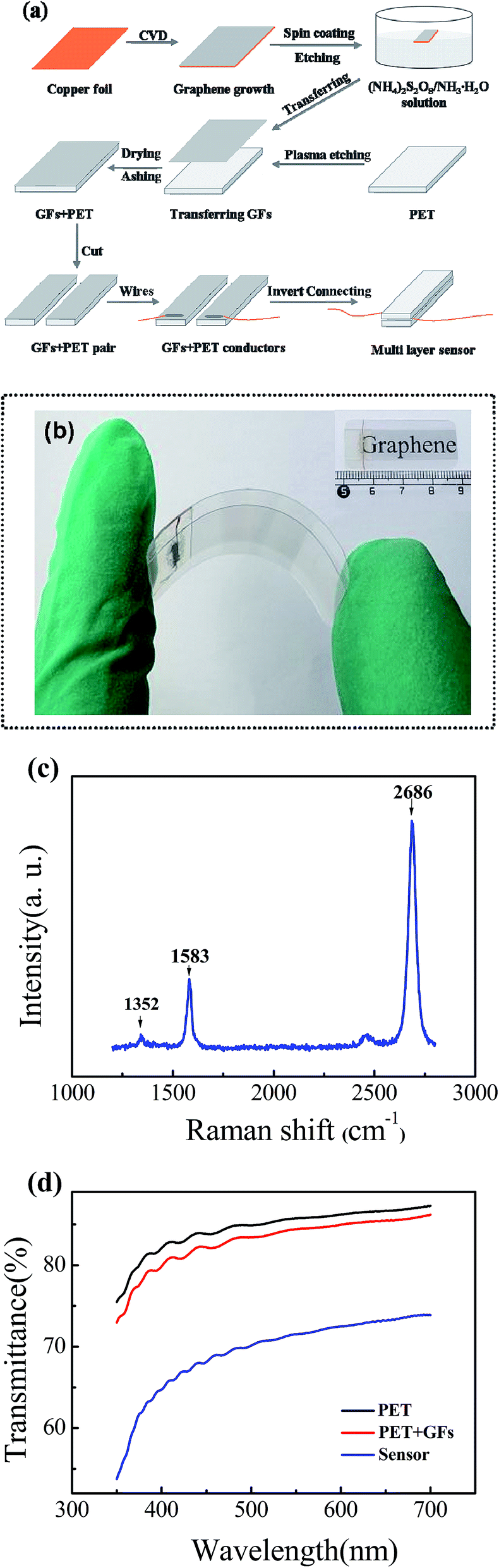 | ||
| Fig. 1 (a) Schematic diagram of fabrication procedure of a tactile sensor based on GFs and PET plate. (b) Optical photograph of a bent assembled sensor. The geometric dimension of the sensor is shown in the inset. (c) Raman shift of the GFs with a typical D ≈ 1352 cm−1, G ≈ 1583 cm−1 and 2D ≈ 2686 cm−1 peak. (d) Transmittance spectra of pure PET, GFs-PET composite structure and multilayer stacked nano-film sensor in the visible wavelength range from 350 to 700 nm. | ||
The Raman spectrum (Horiba JY-HR800) of the graphene films shown in Fig. 1c demonstrates the characteristic peaks of 1352, 1583, and 2686 cm−1, which is correspondence to the D, G, and 2D band of graphene, respectively. As shown in the Raman spectrum, the typical intensity ratio of prominent peak 2D and G (I2D/IG) is approximately greater than 2, which confirmed that the graphene had a single layer structure. The Fig. S2 in the ESI† indicated that the graphene was a continuous film. Fig. 1d depicts the transparency comparison (Technical Institute of Physics and Chemistry CAS) of a pure PET, GFs-PET composite structure and multilayer stacked nano-film sensor, respectively. The optical transmittance of the fabricated sensor is about 70% in the visible range, which provides optical transparency enough for an aesthetic view of the human body. Compared with previously reported wearable sensors, the optical transmittance of our sensors is favorably comparable with recent values of other graphene-based sensors (∼70%),29 and slightly better than those nanocomposite devices (63–68%),30,31 and far superior than that previously reported (<20%).32
Fig. 2a is a schematic illustration of the tactile sensor. As presented in Fig. S3,† though the tactile sensor was multilayered, the total thickness was only about 320 μm (which is around 60% of the thickness of the human epidermis). The resistance variation of the total sensor is monitored during applying constant pressure (a conical shaped indenter weighted 0.25 N) while continuously increasing the distance between pressure and initial tactile.
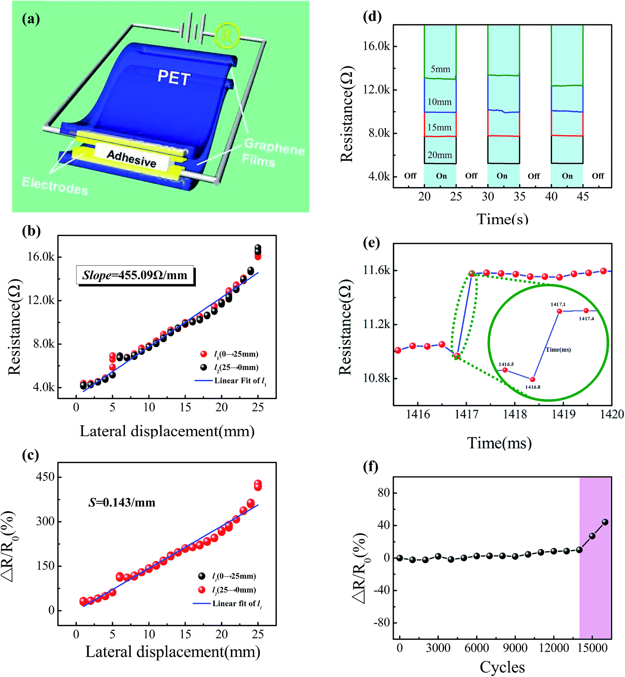 | ||
| Fig. 2 (a) Schematic illustration of the tactile sensor consisting of the stacked nanohybrid structure. (b) A typical sensor's characteristic of resistance change with an increase (red line)/decrease (black line) in distance. (c) Distance-dependent ΔR/R0 of the sensor at distance ranging from 0 mm to 25 mm. (d) Time-dependent resistance change of the sensor in response to distance of 5 mm, 10 mm, 15 mm, and 20 mm at repetitive cycle stress. (e) Time response characteristic of the tactile sensor. According to the enlarged illustration, the response time is 0.3 ms. (f) The stability of the tactile sensor for more than 14000 loading/unloading cycles, at 2 s for each cycle, with an applied pressure of human finger. | ||
The principle of the device for displacement detection is as same as the sliding rheostat. Each device can be treated as a resistor with the resistance R given by:
| R = R1 + R2 + Ra | (1) |
 | (2) |
Fig. 2b shows the tactile sensing function of our sensor. The resistance R is only 3.19 kΩ when the pressure acting on the end of electrode which is defined as the origin tactile l = 0 mm. Then, the resistance of the sensor increases as long as the distance l increases, and at last reached up to 16.87 kΩ at the distance l = 25 mm. Obviously, the resistance R possesses a linear dependence on the distance and the slope of the fitting curve is about 455.09 Ω mm−1. Moreover, the tendency of the two curves show high coincidence between l1 (increase the distance, original state) and l2 (decrease the distance, after 10000 loading cycles), indicating excellent reproducibility. The jump of the curve at 5 mm may be caused by the damage of graphene films. We set R0 for the initial resistance of the sensor when the pressure acting on the origin tactile. ΔR is defined as the deference between the initial resistance R0 and the resistance R measured in real time.
The Fig. 2c shows the fractional change in resistance ΔR/R0 reached up to 420% at the distance l = 25 mm. And ΔR/R0 shows a linear dependence on the pressure tactile. According to previous literature,33 tactile sensitivity S, defined as the slope of the traces, which is commonly used to evaluate the performance of the sensor as below:
 | (3) |
As shown in Fig. 2c, the tactile sensitivity of our sensors is 0.143 mm−1, which means the fractional change in resistance will up to 14.3% when the pressure tactile changes 1 mm.
In the following experiments, several typical pressures tactile such as 5 mm, 10 mm, 15 mm and 20 mm, are measured with a pressure of about 0.25 N. A pressing stimulus was applied by an indenter (m = 25 g) to introduce a contact between the top and bottom GFs-PET conductive plate. Fig. 2d shows the response of the device upon loading/unloading the force and the stable resistance response indicate that the device exhibits an excellent mechanical robustness and the reliability. It is well known fast response time is important in realizing real-time tactile monitoring. Here, the response time (rise time) is defined as the time interval between 10% and 90% of the steady state values of resistance. As shown in the inset of Fig. 2e, the response time of our tactile sensor was estimated to be about 0.3 ms. Compared with previously reported resistive sensors, the response time of our sensors is favorably comparable with recent values of other nanocomposite sensors (0.4 ms),34 and faster than those flexible devices (4–17 ms),29,35–37 and far superior than that previously reported (90–200 ms).38–40 To further investigate the stability of the tactile sensor, the resistance changes of the sensor were measured when repeatedly load/unload an applied pressure of human finger for more than 14000 cycles (2 s for each cycle). The result is shown in Fig. 2f, which reveals that the tactile sensor exhibits high durability. Above all, our fast responsibility sensor is adequate to be used in electronic and circuit system, wearable sensors and mechanical applications.
As a tactile sensor, the response of a device to the tactile of pressure must be specific. That means during the pressure applied only the displacement which is the target detection signal will cause a significant change in resistance. Any other signals caused by pressure, regarded as interference signals such as vertical displacement, stress magnitude, stress acting area and bending strain, can not lead to obvious resistance signal in the detection process. This is the key to ensure the reliability of the accurate tactile.
To investigate the reliability of the devices for tactile sensing, we measured the properties of our sensors under the interference. The anti interference against the longitudinal change of the pressure tactile at the horizontal coordinate of 5, 10, 15 and 20 mm is shown in Fig. 3a. The width of the sensor was 10 mm. The touch points with the same distance from the electrode must have the same resistance. That means if the sensor was in a two-dimensional coordinate system and the touch movement in the X axis will cause the change of resistance while no change in the Y axis. This protects the sensor from output wrong signal while touch movement appeared in the Y axis. The real-time resistance curves had no markedly interference and the fractional change in resistance ΔR/R0 was only 0.1%, which was much lower than the sensitivity of our sensors (14.3%). This result comes from the uniformity of the graphene films that ensures the resistance distribution was uniform.
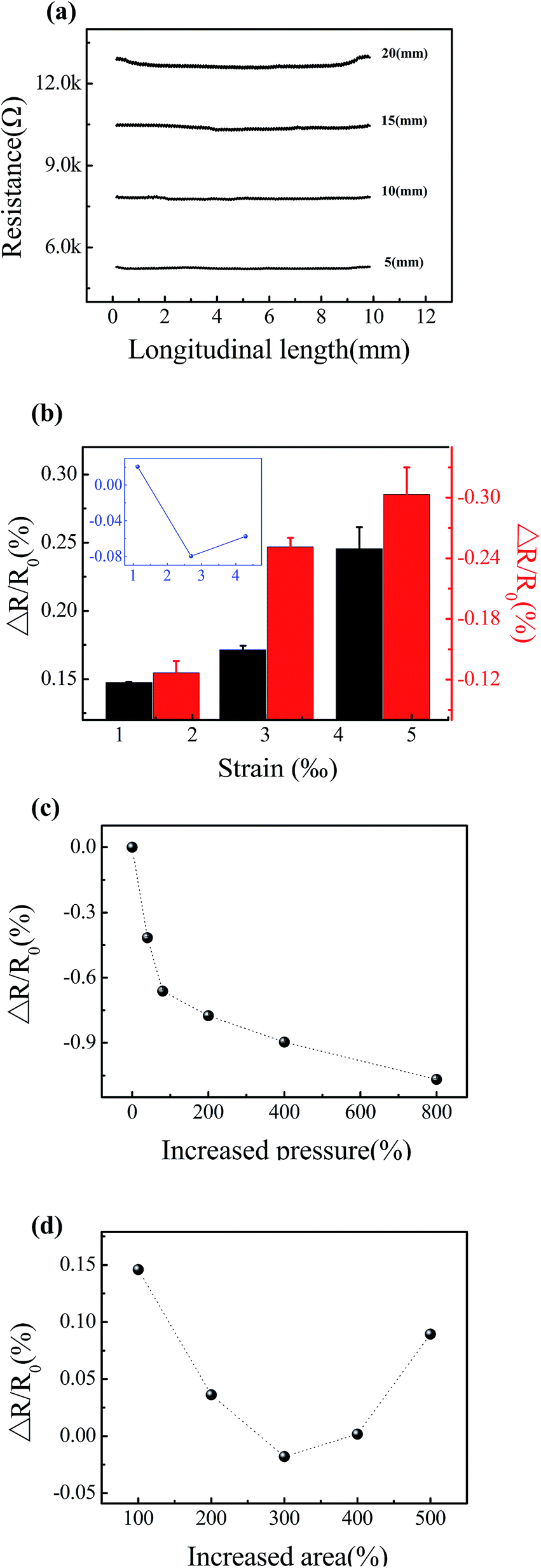 | ||
| Fig. 3 (a) Sensitivity of the device to longitudinal displacement at different axial distance of 5 mm, 10 mm, 15 mm, 20 mm. (b) Stability of the tactile sensor to the applied tension (black column) and compression (red column) strain. (c) Stability of the tactile sensor to the increased pressure. (d) Stability of the tactile sensor to the increased force area. | ||
Fig. 3b presents the immunity of the GFs-PET composite conductor to the tensile (black column) and compressive (red column) strain. The bending test was just for single plate. The resistance of the conductive plate was increased under tensile strain, but decreased under compressive strain. However, the fractional change in resistance ΔR/R0 shows a slight variation (∼0.3%) that is much smaller than the sensitivity of tactile sensing even if the bending strain increases up to 4.3‰. An inset shown in Fig. 3b described the total sensor under bending with the strain from 1.1‰ increasing to 4.3‰. The maximum rate of change in resistance appeared in strain 4.3‰ was only 0.08%, which was even lower than a single conductive plate under the bending strain 1.1‰ (∼0.13%). Because the sensor was a double layer structure, the two conductive plates were always under bend strain with the same value but opposite direction. Therefore, the bend strain of the total sensor was always smaller than that of any one plate.
On the other hand, the resistance responses of sensor to other interfering signals such as stress magnitude (Fig. 3c) and stress acting area (Fig. 3d) were little sensitive. Initial resistance R0, was designated as the resistance at distance of 14 mm where applied a constant pressure of 0.25 N. After the extra pressure increased from 0 to 2 N, the fluctuation of the resistance change rate kept in a very small range (<1.1%). Similarly, we also evaluated the anti interference of the sensor to the stress acting area as shown in Fig. 3d. The stress acting area of slide (2 mm × 15 mm) was defined as original area s, and it was increased up to 5-fold larger by adding up numbers of slides with the same geometric size. In particular, the increase of the stress area is only added to the same side of the initial slide that away from the electrodes, which is to ensure that the effective length l is constant. Ra is the sum of the two graphene films' vertical resistance and the contact resistance between the two layers. The graphene film is a monolayer film so that the carrier scattering in the vertical direction is very small. On the other hand, the plate is not flat on the micrometer scale and the contact of two plates can be seen as numerous “point contact”. Obviously, the contact resistance (affected by the number of contact points) of the two plates makes the greatest contribution to the Ra. So, when the surface area is constant, the number of contact points increases with the pressure increases, this resulting in a slight reduction in sensor resistance. The contact points will increase as the contact area increased, leading to the increase of the carrier number passing through the “contact points” during the unit time, resulting in a slight reduction in the sensor resistance. While the increased bending strains of the plate at the same time will increase the sensor resistance. So the combined result of the two changes in the surface area variation test will be obtained:
 | (4) |
There is a difference of 5Ra/6 compared to the original resistance R given by formula (1). However, the fractional change in resistance ΔR/R0 of area change showed a slight variation (<0.15%) that was much smaller than the sensitivity of tactile sensing (14.3%). Consequently, the results indicate that the tactile sensor has an outstanding anti interference against the stress acting area because the resistance Ra is small enough to be negligible compared to R1 and R2.
Application of the graphene-based tactile sensors for human machine interface (HMI) transmission is demonstrated. The sensor serves as a flexible and transparent touch strip, as shown in Fig. 4. The LED lights were series connected in the circuit, in order to show a significant variation when the pressure finger moved from the finger root to the tip under the bias voltage of 10 V. When the finger moved back, the brightness of LED lights will be restored.
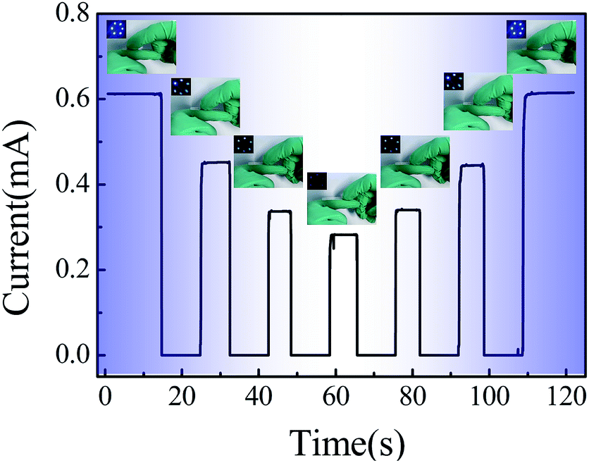 | ||
| Fig. 4 Wearable graphene-based sensor for finger pressure tactile detections. The variation of the LED connected in the external circuit and the finger movements are shown in the illustration. | ||
4. Conclusions
In summary, a wearable tactile sensor was assembled with the multilayer stacked nano-films structure of PET-GFs/GFs-PET. Notably, the graphene-based sensors do not only feature an impressively high sensitivity of 0.143 mm−1 for tactile sensing, but also show the strong anti-interference ability to the interference signals such as vertical displacement, stress magnitude, stress acting area and bending strain. After repeatedly load/unload an applied pressure of 0.25 N for more than 14000 cycles (2 s for each cycle), the sensors still demonstrate the high tactile sensing ability within relative resistance variability of 9.98%. The tactile sensors are able to control electronic circuit with fast response time of ∼0.3 ms, which is fairly comparable or superior to recent studies of other resistive sensors. Prototype devices were also demonstrated by attached the tactile sensor onto a little finger for touch tactile detection. Our sensors have a great advantage in transparency and flexibility when compete with the conventional metal and semiconductor tactile devices. And compared with the recently tactile sensor arrays, the graphene-based device is easy to fabricate and wearable without integration. We believe that the facile, low-cost and readily scalable method allows practical fabrication of graphene-based tactile sensors for emerging human-interactive applications.
Acknowledgements
This work was supported by the National Natural Science Foundation of China (No. 51572025, 51527802 and 51232001), the National Major Research Program of China (No. 2013CB932602), the Program of Introducing Talents of Discipline to Universities (B14003), The Beijing Municipal Science & Technology Commission and the Fundamental Research Funds for Central Universities.References
- S. C. B. Mannsfeld, B. C. K. Tee, R. M. Stoltenberg, C. V. H. H. Chen, S. Barman, B. V. O. Muir, A. N. Sokolov, C. Reese and Z. Bao, Nat. Mater., 2010, 9, 859–864 CrossRef CAS PubMed.
- J. J. Boland, Nat. Mater., 2010, 9, 790–792 CrossRef CAS PubMed.
- K. Takei, T. Takahashi, J. C. Ho, H. Ko, A. G. Gillies, P. W. Leu, R. S. Fearing and A. Javey, Nat. Mater., 2010, 9, 821–826 CrossRef CAS PubMed.
- R. R. Bao, C. F. Wang, L. Dong, R. M. Yu, K. Zhao, Z. L. Wang and C. F. Pan, Adv. Funct. Mater., 2015, 25, 2884–2891 CrossRef CAS.
- C. Bartolozzi, L. Natale, F. Nori and G. Metta, Nat. Mater., 2016, 15, 921–925 CrossRef CAS PubMed.
- Y. Zhang, X. Q. Yan, Y. Yang, Y. H. Huang, Q. L. Liao and J. J. Qi, Adv. Mater., 2012, 24, 4647–4655 CrossRef CAS PubMed.
- J. J. Qi, Y. W. Lan, A. Z. Stieg, J. H. Chen, Y. L. Zhong, L. J. Li, C. D. Chen, Y. Zhang and K. L. Wang, Nat. Commun., 2015, 6, 7430–7437 CrossRef CAS PubMed.
- Y. Zhang, Y. Yang, Y. S. Gu, X. Q. Yan, Q. L. Liao, P. F. Li, Z. Zhang and Z. Z. Wang, Nano Energy, 2015, 14, 30–48 CrossRef CAS.
- B. C. K. Tee, A. Chortos, R. R. Dunn, G. Schwartz, E. Eason and Z. A. Bao, Adv. Funct. Mater., 2014, 24, 5427–5434 CrossRef CAS.
- Y. Wang, L. Wang, T. T. Yang, X. Li, X. B. Zang, M. Zhu, K. L. Wang, D. H. Wu and H. W. Zhu, Adv. Funct. Mater., 2014, 24, 4666–4670 CrossRef CAS.
- Y. Hou, H. Z. Wang, Q. H. Zhang, Y. G. Li and M. F. Zhu, Adv. Mater., 2014, 26, 5018–5024 CrossRef PubMed.
- S. Jung, J. H. Kim, J. Kim, S. Choi, J. Lee, I. Park, T. Hyeon and D. H. Kim, Adv. Mater., 2014, 26, 4825–4830 CrossRef CAS PubMed.
- Q. Sun, D. H. Kim, S. S. Park, N. Y. Lee, Y. Zhang, J. H. Lee, K. Cho and J. H. Cho, Adv. Mater., 2014, 26, 4735–4740 CrossRef CAS PubMed.
- D. J. Lipomi, M. Vosgueritchian, B. C. K. Tee, S. L. Hellstrom, J. A. Lee, C. H. Fox and Z. N. Bao, Nat. Nanotechnol., 2011, 6, 788–792 CrossRef CAS PubMed.
- W. L. Hu, X. F. Niu, R. Zhao and Q. B. Pei, Appl. Phys. Lett., 2013, 102, 083303 CrossRef.
- B. Li, A. K. Fontecchio and Y. Visell, Appl. Phys. Lett., 2016, 108, 013502 CrossRef.
- S. S. Yao and Y. Zhu, Nanoscale, 2014, 6, 2345–2352 RSC.
- J. Lee, H. Kwon, J. Seo, S. Shin, J. H. Koo, C. Pang, S. Son, J. H. Kim, Y. H. Jang, D. E. Kim and T. Lee, Adv. Mater., 2015, 27, 2433–2439 CrossRef CAS PubMed.
- J. Ge, L. Sun, F. R. Zhang, Y. Zhang, L. A. Shi, H. Y. Zhao, H. W. Zhu, H. L. Jiang and S. H. Yu, Adv. Mater., 2016, 28, 722–728 CrossRef CAS PubMed.
- Z. L. Wang, R. S. Yang, J. Zhou, Y. Qin, C. Xu, Y. F. Hu and S. Xu, Mater. Sci. Eng., R, 2010, 70, 320–329 CrossRef.
- W. Z. Wu, X. N. Wen and Z. L. Wang, Science, 2013, 340, 952–957 CrossRef CAS PubMed.
- Z. L. Wang, Adv. Mater., 2012, 24, 4632–4646 CrossRef CAS PubMed.
- C. F. Pan, L. Dong, G. Zhu, S. M. Niu, R. M. Yu, Q. Yang, Y. Liu and Z. L. Wang, Nat. Photonics, 2013, 7, 752–758 CrossRef CAS.
- C. C. Kim, H. H. Lee, K. H. Oh and J. Y. Sun, Science, 2016, 353, 682–687 CrossRef CAS PubMed.
- X. Li, P. Z. Sun, L. L. Fan, M. Zhu, K. L. Wang, M. L. Zhong, J. Q. Wei, D. H. Wu, Y. Cheng and H. W. Zhu, Sci. Rep., 2012, 2, 395–402 Search PubMed.
- K. S. Kim, Y. Zhao, H. Jang, S. Y. Lee, J. M. Kim, K. S. Kim, J. H. Ahn, P. Kim, J. Y. Choi and B. H. Hong, Nature, 2009, 457, 706–710 CrossRef CAS PubMed.
- X. Li, W. Cai, J. An, S. Kim, J. Nah, D. Yang, R. Piner, A. Velamakanni, I. Jung, E. Tutuc, S. K. Banerjee, L. Colombo and R. S. Ruoff, Science, 2009, 324, 1312–1314 CrossRef CAS PubMed.
- S. Bhaviripudi, X. Jia, M. S. Dresselhaus and J. Kong, Nano Lett., 2010, 10, 4128–4133 CrossRef CAS PubMed.
- J. Zhao, G. L. Wang, R. Yang, X. B. Lu, M. Cheng, C. L. He, G. B. Xie, J. L. Meng, D. X. Shi and G. Y. Zhang, ACS Nano, 2015, 9, 1622–1629 CrossRef CAS PubMed.
- E. Roh, B. U. Hwang, D. Kim, B. Y. Kim and N. E. Lee, ACS Nano, 2015, 9, 6252–6261 CrossRef CAS PubMed.
- D. J. Lipomi, M. Vosgueritchian, B. C. K. Tee, S. L. Hellstrom, J. A. Lee, C. H. Fox and Z. N. Bao, Nat. Nanotechnol., 2011, 6, 788–792 CrossRef CAS PubMed.
- X. Xiao, L. Yuan, J. Zhong, T. Ding, Y. Liu, Z. Cai, Y. Rong, H. Han, J. Zhou and Z. L. Wang, Adv. Mater., 2011, 23, 5440–5444 CrossRef CAS PubMed.
- N. S. Lu, C. Lu, S. X. Yang and J. Rogers, Adv. Funct. Mater., 2012, 22, 4044–4050 CrossRef CAS.
- H. Tian, Y. Shu, X. F. Wang, M. A. Mohammad, Z. Bie, Q. Y. Xie, C. Li, W. T. Mi, Y. Yang and T. L. Ren, Sci. Rep., 2015, 5, 8603–8608 CrossRef CAS PubMed.
- M. Ha, S. Lim, J. Park, D. S. Um, Y. Lee and H. Ko, Adv. Funct. Mater., 2015, 25, 2841–2849 CrossRef CAS.
- X. W. Wang, Y. Gu, Z. P. Xiong, Z. Cui and T. Zhang, Adv. Mater., 2014, 26, 1336–1342 CrossRef CAS PubMed.
- S. Gong, W. Schwalb, Y. Wang, Y. Chen, Y. Tang, J. Si, B. Shirinzadeh and W. Cheng, Nat. Commun., 2014, 5, 3132–3139 Search PubMed.
- S. Harada, W. Honda, T. Arie, S. Akita and K. Takei, ACS Nano, 2014, 8, 3921–3927 CrossRef CAS PubMed.
- K. Takei, Z. Yu, M. Zheng, H. Ota, T. Takahashi and A. Javey, Proc. Natl. Acad. Sci. U. S. A., 2014, 111, 1703–1707 CrossRef CAS PubMed.
- C. L. Choong, M. B. Shim, B. S. Lee, S. Jeon, D. S. Ko, T. H. Kang, J. Bae, S. H. Lee, K. E. Byun, J. Im, Y. J. Jeong, C. E. Park, J. J. Park and U. I. Chung, Adv. Mater., 2014, 26, 3451–3458 CrossRef CAS PubMed.
Footnote |
| † Electronic supplementary information (ESI) available. See DOI: 10.1039/c7ra04239f |
| This journal is © The Royal Society of Chemistry 2017 |