
 Open Access Article
 This Open Access Article is licensed under a Creative Commons Attribution-Non Commercial 3.0 Unported Licence
Enhanced transmittance and piezoelectricity of transparent K0.5Na0.5NbO3 ceramics with Ca(Zn1/3Nb2/3)O3 additives
Qizhen Chai,
Xumei Zhao,
Xiaolian Chao* and
Zupei Yang *
*
Key Laboratory for Macromolecular Science of Shaanxi Province, Shaanxi Key Laboratory for Advanced Energy Devices, School of Materials Science and Engineering, Shaanxi Normal University, Xi’an, 710062, Shaanxi, China. E-mail: yangzp@snnu.edu.cn; chaoxl@snnu.edu.cn; Fax: +86-29-8153-0702; Tel: +86-29-8153-0703
First published on 30th May 2017
Abstract
Considering the environment and human health, highly transparent lead-free (1 − x)K0.5Na0.5NbO3–xCa(Zn1/3Nb2/3)O3 (abbreviated as KNN–xCZN) piezoceramics were synthesized by a solid state reaction method. The effects of Ca(Zn1/3Nb2/3)O3 on the microstructures, phase structures, characteristic frequency and electrical properties were investigated. Fine grain and relaxor-like behaviors were obtained, and the Ca(Zn1/3Nb2/3)O3 also increased the crystal structure of the ceramics transformation from orthorhombic to pseudo-cubic. It was found that the highest transmittance of 70.42% (with a thickness of 0.5 mm in the visible spectrum) was obtained for the KNN–xCZN ceramics at x = 0.07, which was due to the high relative density, low apparent porosity, uniform and fine-grained microstructures, high symmetry of the pseudo-cubic structure, NbO6 octahedron reduced distortion and more relaxor-like behavior. In addition, the transparent piezoelectric ceramics KNN–xCZN with x = 0.07 possessed high transmittance (∼84% at near-infrared wavelengths) and excellent electrical properties (er = 1162, d33 = 102 pC N−1). All of the above demonstrated that the KNN–xCZN ceramics could be promising lead-free transparent piezoceramics.
Introduction
Transparent lead-free piezoceramics are a new type of important environmentally friendly functional material, which are fiercely competitive in the international material field.1–3 They are highly likely to be the key material for light, computer and electronic information technologies and national defense military applications in the future.4–7 In addition, most transparent piezoelectric ceramics could be used for energy storage.8After the discovery of transparency in 0.8(K0.5Na0.5)NbO3−0.2SrTiO3 ceramics was reported by Malic et al. in 2004,9 K0.5Na0.5NbO3 lead-free transparent piezoelectric materials have attracted the attention of many researchers (the development is shown in Fig. 1). These research results indicate that K0.5Na0.5NbO3 lead-free materials are expected to replace lead-based ceramics in terms of the transparent characteristic. However, the transmittance conflicts with the piezoelectric properties since these properties of piezoelectric ceramics originate from the asymmetry of the crystal structure. As a consequence and in theory, there is difficulty obtaining high transmittance due to the crystal structure in piezoelectric ceramics. So research on the excellent performance of piezoelectric ceramics with high transmittance is in demand. Two methods are mainly used to solve this issue: one is ion substitution modification and the other is advanced technologies. The influence of the latter on property enhancement is limited due to the high cost.9–11
 | ||
| Fig. 1 The development of KNN-based transparent ceramics. | ||
A previous study showed that the substitution of some aliovalent ions at the A site could promote the piezoelectric properties of KNN materials because of the different defect structure and improvement of the microstructure.12–14 For example, an extra electron (e−) can be easily generated for keeping the valence balance when Ba2+ is used to replace the A site of KNN-based materials (see eqn (1)).15
 | (1) |
At the same time, the K+ vacancy is formed due to the evaporation of K+ during processing and preparation,16 as shown in eqn (2).
 | (2) |
The vacancy and electron would be easily recombined and eliminated during processing, which results in increasing resistivity. In addition, aliovalent metals are often used to tailor the electrical properties of KNN materials by forming point defects17–20 at the Nb site. It is usually accepted that the defect dipoles formed by the acceptor dopants for charge balance will prohibit domain-wall motion and Cu-modified KNN systems have been extensively studied.21–23
Ca and Ba are in the same main group and Zn and Cu are in the same period, also Na+ (1.02 Å) and Nb5+ (0.64 Å) would tend to be replaced by Ca2+ (1.00 Å) and Zn2+ (0.74 Å), respectively, due to their similar radii. Therefore, in the ABO3 perovskite structure, Ca2+ and Zn2+ are suitable for being introduced to the A and B sites, respectively.
Here, considering the above factors, Ca(Zn1/3Nb2/3)O3 was doped in the KNN ceramics, and the effects of the concentration of Ca(Zn1/3Nb2/3)O3, x, on the microstructures, phase structures, optical properties and electrical properties have been investigated in detail. Furthermore, KNN–xCZN ceramics were fabricated by a pressureless ceramics processing procedure and the transparent mechanism was also discussed in this work.
Results and discussion
Fig. 2 shows the transparency of the (1 − x)KNN–xCZN (x = 0.03, 0.05, 0.06, 0.07, 0.08, 0.10) ceramics. The thickness of the samples is 0.5 mm. The optical transmittance (T) of 0.93KNN–0.07CZN is shown in Fig. 2(a), indicating that the transmission is close to 80% at near-infrared wavelengths and about 70% in the visible region. The photographs of the highly transparent 0.93KNN–0.07CZN ceramics are shown in the inset of Fig. 2(a). In the photographs, the lake, flowers and buildings can be easily seen through the samples. The optical transmittance of (1 − x)KNN–xCZN for light at wavelengths 1064 nm and 780 nm can be attained from Fig. 2(b). The letters behind the (1 − x)KNN–xCZN (x = 0.03, 0.05, 0.06, 0.07, 0.08, 0.10) ceramics can be clearly read, suggesting that the samples have novel transparencies in the visible region, which is shown in the photograph of the 0.5 mm-thick ceramics in the inset of Fig. 2(b). Moreover, as is observed from Fig. 2(b), with x increasing from 0.03 to 0.10, the transmittance first increases and then decreases and the maximum optical transmittance appears at x = 0.07. The high transparency of the 0.93KNN–0.07CZN ceramics could be attributed to the small grain size (mean size is close to 200 nm), low porosity, crystal structure and relaxor behavior. These results will be discussed in a later section. | ||
| Fig. 2 Transmission spectra of the (1 − x)KNN–xCZN ceramics. (a) Transmittance of the 0.93KNN–0.07CZN specimen and the photographs in the inset and (b) the optical transmittance of (1 − x)KNN–xCZN for light at wavelengths 1064 nm and 780 nm, and the photographs (the specimens with x = 0.03, 0.05, 0.06, 0.07, 0.08, 0.10 from left to right above the letters) in the inset. The thickness of the samples is 0.5 mm. | ||
In addition, the transmittance decreases gradually to near zero at 400 nm and below. This can be attributed to the interband transition according to the results reported by Zhao Wang et al.25 The optical band gap energy (Eg) is very critical to the optical characteristics study, which can be estimated from the absorption spectra according to the Tauc equation.26 As for the direct transition, the relationship of Eg, ν (photon frequency), h (4.1357 × 10⁻¹⁵ eV, Planck’ constant), and A (a constant) is given as:
| (αhν)2 = A(hν − Eg) | (3) |
The photon frequency ν and absorption coefficient α can be calculated by the given formulas:
 | (4) |
 | (5) |
 | ||
| Fig. 3 (a and b) Plot of (αhν)2 versus hν for the (1 − x)KNN–xCZN ceramics. The insets show the photo energy hν ranges of 2.0–3.3 eV and 2.5–3.3 eV, respectively. (c) The band gap energy Eg of (1 − x)KNN–xCZN ceramics. | ||
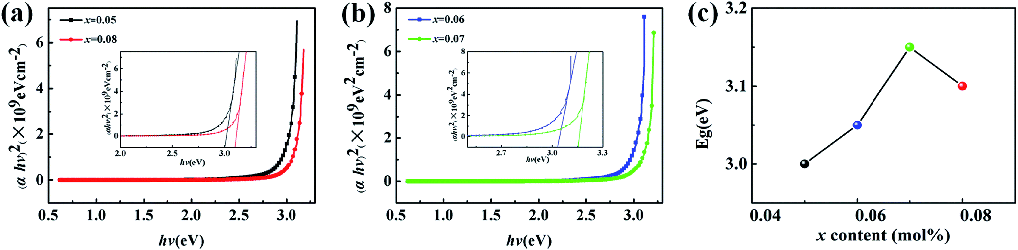
The band gap Eg of (1 − x)KNN–xCZN ceramics (x = 0.05, 0.06, 0.07 and 0.08) was obtained from the curve in the inset of Fig. 3(a) and (b) (Eg = 3.0 eV, 3.05 eV, 3.15 eV and 3.10 eV), suggesting that the modifier, Ca(Zn1/3Nb2/3)O3, has an obvious effect on the ceramics band-gap. Fig. 3(c) exhibits the Eg of (1 − x)KNN–xCZN ceramics with different x. The highest Eg reaches 3.15 eV when x = 0.07, which is higher than the value (3.09 eV) of the highest transmittance in (K0.5Na0.5)0.95Li0.05Nb0.95Bi0.05O3 transparent ceramics in previous reports.27–29 Generally, the larger the Eg value, the higher the transparency.24 The reason can be briefly explained as follows. Electrons can be excited from the valence band to the conduction band by light only if it has enough energy. In this process, part of the light is used for electronic transition, the rest can transmit, scatter and so on. The large Eg value is likely to increase the difficulty of electronic leaps into the conduction band. When the light source is not enough to excite the electronic transition, more energy is used for transmitting, which leads to a higher transparency, while the light loss is relatively small.
The surface morphology of the KNN–xCZN ceramics with different concentrations was measured using a scanning electron microscope (SEM) as shown in Fig. 4. All samples (particularly the sample of x = 0.07) clearly exhibit dense microstructures (a low porosity), which is conducive to enhancing the transmittance (T) of samples. In order to further identify the influence of CZN concentration on the grain size distribution and relative density, the columnar maps of the grain size distribution and the line charts of the mean size and relative density are shown in Fig. 5. When increasing the Ca(Zn1/3Nb2/3)O3 content, the mean grain sizes (which were calculated on the basis of the grain size distribution) of the (1 − x)KNN–xCZN ceramics decrease and then increase after reaching a minimum at x = 0.07. The changing tendency of the relative density is opposite to that of the average grain sizes, as shown in Fig. 5(b). The average grain sizes of the (1 − x)KNN–xCZN specimens are 265.8, 236.2, 207.5, 195.1, 201.2 and 204.9 nm for x = 0.03, 0.05, 0.06, 0.07, 0.08 and 0.10, respectively. The relative densities are 93.1, 95.3, 96.6, 98.3, 97.5 and 96.7% for x = 0.03, 0.05, 0.06, 0.07, 0.08 and 0.10, respectively. The optical transmittances of (1 − x)KNN–xCZN in the visible region (shown in Fig. 2 at 780 nm) are 50.2, 58.3, 61.5, 70.4, 66.2 and 63.0 for x = 0.03, 0.05, 0.06, 0.07, 0.08 and 0.10, respectively. Hence it can be deduced that a smaller and well-distributed grain is an important factor in transparency, as these grains are too small to cause serious scattering and reflection according to the Tyndall effect.30 In addition, the high density (low porosity) microstructure also plays a crucial role in obtaining the high transparency, due to the high scattering of pores.24
 | ||
| Fig. 4 SEM images of the natural surface microstructures of the (1 − x)KNN–xCZN ceramics. | ||
 | ||
| Fig. 5 (a) Grain size distribution of the (1 − x)KNN–xCZN samples. (b) Dependence of the mean size and the relative density on the composition x. | ||
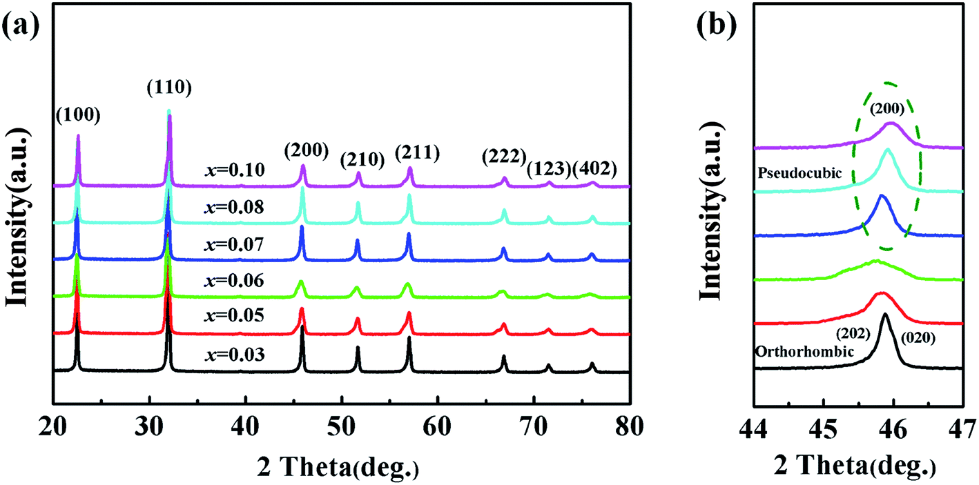
Fig. 6(a) shows the characteristics of the XRD patterns, from which the pure perovskite phase of the ceramics for x = 0.03–0.10 can be observed. It could be concluded that CZN completely diffused into the KNN lattice and the KNN–xCZN ceramics of the perovskite-type solid solution were obtained. Moreover, Fig. 6(b) shows the split (200) peak between 44° and 47°, from which the changes of the phase structure between x = 0.06–0.07 can be seen. The (202)/(020) peak splitting characterizes the orthorhombic phase and the single (200) peak characterizes the pseudo-cubic phase at about 45.5°.31 As can be seen from Fig. 6(b), the split (202)/(020) peaks faded away with the increasing CZN concentration, demonstrating that the crystal structure of the KNN–xCZN ceramics has orthorhombic symmetry at x = 0.03, 0.05 and 0.06, and a pseudo-cubic phase at x = 0.07, 0.08 and 0.10.8 The interpretation is based on a conventional structure model and no attempts are made to take into account the presence of any intermediate phase. Then it can be concluded that the phase transition from orthorhombic to pseudo-cubic symmetry was caused by the increasing CZN concentration. The ceramics of symmetrical pseudo-cubic phase have minimal optical anisotropy, which leads to a decrease of the light scattering and increase of the optical transmittance.
 | ||
| Fig. 6 (a) XRD patterns of the (1 − x)KNN–xCZN ceramics. (b) The amplified XRD patterns at 2θ = 44–47° of the (1 − x)KNN–xCZN ceramics. | ||
To further confirm the effect of CZN concentration on the lattice parameters of the KNN–xCZN samples, the lattice constants of the (1 − x)KNN–xCZN ceramics with different CZN concentration are shown in Fig. 7. For the (1 − x)KNN–xCZN ceramics, the calcium ion has a different valence from the potassium and sodium ions. Besides, the phase transition and structural framework are distorted by the zinc and niobium ions. The dielectric spectra (Fig. 9) can further confirm the interpretation. Moreover, the least squares method is used to calculate the lattice parameters of a, b, and c from the XRD data. The values of Δ(a − b) and Δ(b − c) become smaller with increasing x from 0.03 to 0.10, which further demonstrates that the phase structure evolves from the orthorhombic to pseudo-cubic phase at room temperature. Furthermore, the value of a/c at x = 0.07 is closer to 1. It is reasonable to conclude that the crystal symmetry of KNN–xCZN ceramics improves with increasing x from 0.03 to 0.10, which is an obviously important segmental reason for the excellent transmittance.
 | ||
| Fig. 7 The lattice parameters of the KNN–xCZN ceramics. | ||
Raman spectroscopy is an effective method to identify the changes of the composition and crystal structure of the KNN-based systems, even for small distortions of the crystal lattice.32,33 Fig. 8 shows the Raman spectra of KNN–xCZN measured at room temperature. The main vibration modes (V1–V5) are correlative with the NbO6 octahedron. The peaks below 200 cm−1 are consistent with the translational mode of the K+/Na+ translation and the rotations of the NbO6 octahedron.34 Fig. 8(b) demonstrates the fitting results of V1 and V2 modes using the Gauss function. The V1 mode can be distributed to the symmetric stretching mode of the NbO6 octahedra, which is consistent with the subtle differences of the Nb–O bond distances. As a result, the V1 mode is susceptive to a slight change of the phase structure and composition.35 Fig. 8(c) demonstrates that increasing the Ca(Zn1/3Nb2/3)O3 content leads to the V1 mode shifting to a lower frequency for the KNN–xCZN ceramics. This is due to the distortion of the NbO6 octahedron reducing, which results in an increase of the crystal symmetry. Moreover, the full width at half maximum (FWHM) of the V1 mode can be used to illustrate the degree of relaxor dispersion. The FWHM of the V1 mode with different values of x is shown in Fig. 8(d). As the concentration of CZN increased from 0.05 to 0.07, the V1 mode became broader, illustrating that the degree of relaxor dispersion of the KNN–xCZN (x = 0.05–0.07) ceramics is enhanced. For the relaxor KNN–xCZN ferroelectric, the reduced light scattering leads to an increase in the optical transparency.36
 | ||
| Fig. 8 (a) Raman spectra of the (1 − x)KNN–xCZN ceramics. (b) The V1 and V2 modes fitted using the Gauss function of the (1 − x)KNN–xCZN ceramics. (c) The dependence of the Raman shift of the V1 mode on the composition of x. (d) The dependence of FWHM of the V1 mode on the composition of x. | ||
Fig. 9 shows the frequency and temperature dependencies of the dielectric constant and the corresponding loss of the KNN–xCZN ceramics measured at frequencies of 1 kHz, 100 kHz, and 100 kHz and in the temperature range of 30 °C to 500 °C. According to Fig. 9(a)–(c), two dielectric peaks can be seen, representing the phase transitions of the cubic phase to tetragonal phase and the tetragonal phase to orthorhombic phase from a high temperature to a low temperature respectively. Fig. 9(d)–(f) show that a single peak is formed from the two dielectric peaks, which demonstrates that the phase of the KNN–xCZN ceramics has transformed completely into pseudo-cubic. This result demonstrates the change of the phase structure in the KNN–xCZN ceramics with the CZN concentration increasing at room temperature, which corresponds to the results of XRD in Fig. 6. The dielectric losses of all specimens are less than 2% from 0 °C to 250 °C, which is favorable for bulk ceramics. Furthermore, the appearance of the diffuse phase transition (DPT) (in Fig. 9) demonstrates that KNN–xCZN ceramics have a relaxation ferroelectric behavior.8
 | ||
| Fig. 9 Temperature and frequency dependency of dielectric permittivity and the corresponding loss for the (1 − x)KNN–xCZN ceramics. | ||
Fig. 10 shows the variable frequency impedance spectra measured at 500 °C to further research the relaxation mechanisms of the KNN–xCZN ceramics. The ceramics with x = 0.05, 0.06, 0.07 and 0.08 all possess distorted Debye-like semicircles, and the intercept at the Z′ axis at low frequency represents the total resistivity of the samples. It is evident that the resistivity of the samples initially increases and then decreases with the increasing Ca(Zn1/3Nb2/3)O3 concentration. Markedly, the maximum resistivity obtained at x = 0.07 is over 1.5 × 10⁷ Ω cm at 500 °C. It is highly likely that the highest grain boundary volume is obtained at x = 0.07 due to it having the smallest grain size, which led to the largest resistivity.
 | ||
| Fig. 10 Impedance spectra of the (1 − x)KNN–xCZN ceramics at 500 °C. The upper inset shows the impedance spectra of 0.93KNN–0.07CZN. | ||
Complex electric modulus analysis, extensively used in the dielectric system, could illuminate the relaxation process that correlated to the conductivity of the ions in the ceramics.37–39 The reciprocal of the complex dielectric constant (ε*) is used to define the complex electric modulus (M*), M* = 1/ε* which is quantified and calculated by the followed equation,
 | (6) |
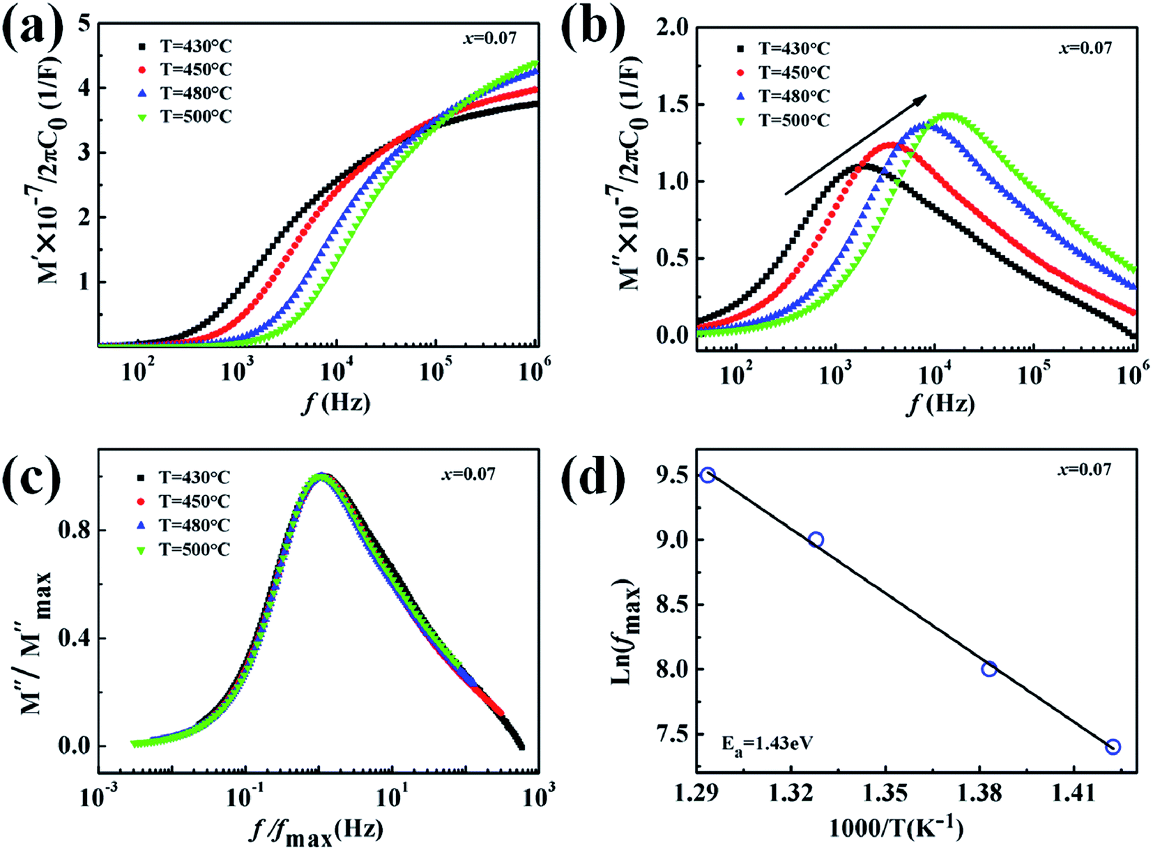 | ||
| Fig. 11 (a and b) M′and M′′ of the x = 0.07 ceramics. (c) The normalized plots of M′′ versus the frequency of the 0.93KNN–0.07CZN ceramics. (d) ln(fmax) vs. 1000/T of the x = 0.07 ceramics (signs: the value of Ea of 0.93KNN–0.07CZN ceramics). | ||
The normalized plot of M′′ versus the frequency is shown in Fig. 11 (c). These curves, obtained from different temperatures, overlap into a single curve suggesting a perfect relaxation process and the other factors can be ignored. The relationship between the activation energy (Ea) related with the relaxation process, Boltzmann constant (k), absolute temperature (T), and pre-exponential factor (f0), is given as39
 | (7) |
According to eqn (7), the activation energy (Ea) can be estimated from a straight line plot of ln(fmax) vs. 1000/T. As shown in Fig. 11(d), the value of Ea of the 0.93KNN–0.07CZN ceramics is 1.43 eV and is obtained from the slope of this fitted straight line. This indicated that the defects’ (such as the oxygen vacancies) influence on the property was weak, and the optical transparency of the KNN–xCZN ceramics was improved.40 In addition, the activation energy of the 0.93KNN–0.07CZN ceramics is less than half of the band-gap energy (see Fig. 3), elucidating that the ceramics exhibit extrinsic band-type conduction.
Fig. 12 (a) shows the relationship between the components, dielectric properties, and phase structure. It can be clearly observed that the maximum values of the relative dielectric permittivity (emax) and the ferroelectric–paraelectric phase transition temperature (Tc) decrease monotonically with the doping amount of CZN increasing from 0.03 to 0.10. The value of emax decreases from 1501 to 1338, 1250, 1162, 1102 and 900 and Tc decreases from 341 to 258, 184, 170, 116 and 53 °C for the (1 − x)KNN–xCZN ceramics when x = 0.03, 0.05, 0.06, 0.07, 0.08, and 0.10, respectively. Fig. 12 (b) shows the relationship between the components, transmittance, piezoelectric constant, and the phase structure. It can be clearly seen that the piezoelectric constant (d33) decreases from 131 to 120, 112, 102, 96 and 80 pC N−1 when x = 0.03, 0.05, 0.06, 0.07, 0.08, and 0.10, respectively and the transmittance initially increases and then decreases with x increasing from 0.03 to 0.10, and when x = 0.07, the sample shows the maximum value. Furthermore, the green interface diagram (x = 0.06) demonstrates that the phase structure changes from orthorhombic to pseudo-cubic phase, which is also indicated in Fig. 6, 7 and 9. These results demonstrate that the additives of Ca(Zn1/3Nb2/3)O3 enhance the optical and electrical properties, particularly the piezoelectricity. The reasons are that, as discussed before, the relative density is high, the apparent porosity is low, the microstructures are uniform and fine-grained, the crystal structure is highly symmetrical, and the sample has a relaxor-like behavior, which are obtained with addition of Ca(Zn1/3Nb2/3)O3. The minimum grain, high symmetrical pseudo-cubic phase, and relaxor-like behavior were obtained for the sample with x = 0.07, which led to the highest transmittance and excellent electrical properties. Based on comprehensive consideration, the 0.93KNN–0.07CZN ceramics can be considered to be promising lead-free transparent piezoelectric candidates.
 | ||
| Fig. 12 (a) The relationship between the maximum relative dielectric constant, ferroelectric–paraelectric phase transition temperature, phase structure and Ca(Zn1/3Nb2/3)O3 content. (b) The relationship between the transparency, piezoelectric constant, phase structure, and the Ca(Zn1/3Nb2/3)O3 content. | ||
Experimental
Synthesis of KNN–xCZN via solid state sintering process
The (1 − x)(K0.5Na0.5)NbO3–xCa(Zn1/3Nb2/3)O3 (x = 0.03, 0.05, 0.06, 0.07, 0.08, 0.10) ceramics in this study were prepared by the solid state reaction method. The method mainly consisted of five steps and the detailed method can be found in our previous literature.24 Firstly, the starting materials, including K2CO3, Na2CO3, Nb2O5, CaCO3, ZnO of 99.99% purity, were dried and then weighed to prepare KNN–xCZN with different values of x according to the stoichiometry followed by milling for 24 h. Secondly, the mixtures were dried and calcined at a temperature of 850 °C for 5 h and then the calcined powders were ball-milled for a second time for 24 h. After drying and then granulating by adding polyvinyl alcohol, the powders were pressed into a plate-shape. Finally, these pellets were heated at 500 °C for 2 h in air to remove the adhesive (PVA), and were then sintered at 1180 °C for 6 h.Characterization of KNN–xCZN
Most of the characterization methods of KNN–xCZN were the same as the previous study,24 including characterising the phase structure, density, microstructure, optical transmittance and dielectric properties. Besides, the Raman spectra (Renishaw, invia) were recorded for characterizing the crystal structure. An impedance analyzer (4294A; Agilent Technologies, Santa Clara, CA) was used to measure the weak-field dielectric responses of the ceramics at temperatures rising from 30 °C to 500 °C with a heating rate of 3 °C min−1. A quasistatic piezoelectric d33 meter (ZJ-3d, Institute of Acoustics Academic Sinica, Beijing, China) was used to measured the piezoelectric coefficient (d33) of 1 day-aged samples (after they were polled in silicone oil at 3 kV mm−1 for half an hour at 80 °C).Conclusions
In summary, transparent piezoelectric ceramics with both high optical transparency and excellent electrical properties have been successfully synthesized. CZN doping can significantly affect the microstructure, phase transition, optical properties and electrical properties. The ceramics with high relative density, low apparent porosity, and uniform and fine-grained microstructures were obtained with addition of Ca(Zn1/3Nb2/3)O3. Moreover, the crystal structure of the ceramics transformed from orthorhombic to pseudo-cubic at x = 0.06. It is confirmed that the transparency variation (in the wavelength range of 400–1600 nm) depended on the microstructure and crystal structure. In addition, the dielectric and piezoelectric properties of KNN–xCZN ceramics were also studied to confirm the relationship between the transparency and relaxor-like behavior. The resistivity of the x = 0.07 ceramics was 1.5 × 10⁷ Ω cm at 500 °C. These results indicate that (1 − x)KNN–xCZN ceramics could be a new type of lead-free transparent piezoelectric ceramics.Acknowledgements
This work was supported by the National Science Foundation of China (NSFC) (Grant No. 51572163, 51577111 and 21401123), the Key Project of Natural Science Foundation of Shaanxi Province (2015JZ011), the Fundamental Research Funds for the Central Universities (Program No. GK201601003), the Information Materials and Devices Research Center of the Shanghai Institute of Ceramics of the Chinese Academy of Sciences (SICCAS) (KLIFMD-2015-04), and the Fundamental Research Funds for the Central Universities (Program No. 2016TS062).Notes and references
- J. Kroupa, J. Petzelt, B. Malic and M. Kosec, J. Phys. D: Appl. Phys., 2005, 38, 679–681 CrossRef CAS.
- H. X. Fu and R. E. Cohen, Nature, 2000, 403, 281 CrossRef CAS PubMed.
- A. B. Haugen, G. H. Olsen, F. Madaro, M. I. Morozov, G. Tutuncu, J. L. Jones, T. Grande and M. A. Einarsrud, J. Am. Ceram. Soc., 2014, 97(12), 3818–3825 CrossRef CAS.
- E. Mensur-Alkoy, A. Berksoy-Yavuz and S. Alkoy, J. Am. Ceram. Soc., 2014, 97(11), 3425–3433 CrossRef CAS.
- W. W. Wu, L. Cheng, S. Bai, W. Dou, Q. Xu, Z. Y. Wei and Y. Qin, J. Mater. Chem. A, 2013, 1, 7332 CAS.
- S. Zhang, R. Xia, L. Lebrun, D. Anderson and T. R. Shrout, Mater. Lett., 2005, 59, 3471–3475 CrossRef CAS.
- H. E. Mgbemere, M. Hinterstein and G. A. Schneider, J. Am. Ceram. Soc., 2013, 96(1), 201–208 CrossRef CAS.
- B. Y. Qu, H. L. Du and Z. Yang, J. Mater. Chem. C, 2016, 4, 1795–1803 RSC.
- K. Marija, V. Bobnar, M. Hrovat, J. Bernard, B. Malic and J. Holc, J. Mater. Res., 2004, 19(6), 1849–1854 CrossRef.
- J. F. Li, K. Wang, B. P. Zhang and L. M. Zhang, J. Am. Ceram. Soc., 2006, 89(2), 706–709 CrossRef CAS.
- R. Gaur, K. C. Singh and R. Laishram, J. Mater. Sci., 2013, 48, 5607–5613 CrossRef CAS.
- M. Ichiki, L. Zhang, M. Tanaka and R. Maeda, J. Eur. Ceram. Soc., 2004, 24, 1693–1697 CrossRef CAS.
- J. J. Zhou, J. F. Li and X. W. Zhang, J. Mater. Sci., 2012, 47, 1767–1773 CrossRef CAS.
- H. Cheng, W. Zhou, H. Du, F. Luo, D. Zhu and B. Xu, J. Mater. Sci., 2014, 49, 1824–1831 CrossRef CAS.
- I. W. Chen and X. H. Wang, Nature, 2000, 404, 168–171 CrossRef CAS PubMed.
- F. Li and K. W. Kwok, J. Eur. Ceram. Soc., 2013, 33, 123–130 CrossRef CAS.
- K. Li, F. L. Li, Y. Wang, K. W. Kwok and H. L. W. Chan, Mater. Chem. Phys., 2011, 131, 320–324 CrossRef CAS.
- F. Z. Yao, K. Wang and J. F. Li, J. Appl. Phys., 2013, 113(17), 174105 CrossRef.
- X. Sun, J. Chen, R. Yu, C. Sun, G. Liu, X. Xing and L. Qiao, J. Am. Ceram. Soc., 2009, 92(1), 130–132 CrossRef CAS.
- Y. F. Chang, S. Poterala, Z. P. Yang and G. L. Messing, J. Am. Ceram. Soc., 2011, 94(8), 2494–2498 CrossRef CAS.
- L. Y. Wang, W. Ren, P. Shi, X. F. Chen, X. Q. Wu and X. Yao, Appl. Phys. Lett., 2010, 97, 072902 CrossRef.
- X. Huang, D. Xiao, X. Li, W. Wu, W. Liang, R. Xie and J. Zhu, J. Am. Ceram. Soc., 2010, 93(9), 2563 CrossRef CAS.
- Y. Kizaki, Y. Noguchi and M. Miyayama, Appl. Phys.Lett., 2006, 89(14), 142910 CrossRef.
- Z. Y. Yang, X. S. Zhang, D. Yang, B. Yang, X. L. Chao, L. L. Wei and Z. P. Yang, J. Am. Ceram. Soc., 2016, 99, 2055–2062 CrossRef CAS.
- Z. Wang, H. S. Gu, Y. M. Hu, K. Yang, M. Z. Hu, D. Zhou and J. G. Guan, CrystEngComm, 2010, 12, 3157–3162 RSC.
- Y. F. Chang, Z. P. Yang, M. Y. Dong, Z. H. Liu and Z. L. Wang, Mater. Res. Bull., 2009, 44, 538 CrossRef CAS.
- S. D. Ross, J. Phys. C: Solid State Phys., 1970, 3, 1785 CrossRef CAS.
- T. Matsuoka, H. Kozuka, K. Kitamura, H. Yamada, T. Kurahashi, M. Yamazaki and K. Ohbayashi, J. Appl. Phys., 2014, 116(15), 154104 CrossRef.
- Y. B. Wei, Z. Wu, Y. M. Jia, J. Wu, Y. C. Shen and H. S. Luo, Appl. Phys. Lett., 2014, 105(4), 042902 CrossRef.
- S. M. Ke, H. T. Huang, H. Q. Fan, H. K. Lee, L. M. Zhou and Y. W. Mai, Appl. Phys. Lett., 2012, 101(8), 082901 CrossRef.
- K. C. Huang, T. C. Huang and W.-F. Hsieh, Inorg. Chem., 2009, 48, 9180 CrossRef CAS PubMed.
- K. Kakimoto, K. Akao, Y. Guo and H. Ohsato, Jpn. J. Appl. Phys., Part 1, 2005, 144, 7064–7067 CrossRef.
- R. Chang, S. Chu, Y. Lin, C. Hong and Y. Wong, J. Eur. Ceram. Soc., 2007, 27, 3360–4453 Search PubMed.
- Z. Y. Liu, H. Q. Fan and B. L. Peng, J. Mater. Sci., 2015, 50, 7958–7966 CrossRef CAS.
- Y. Guo, K. Kakimoto and H. Ohsato, J. Phys. Chem. Solids, 2004, 65, 1831–1835 CrossRef CAS.
- J. G. Wu, D. Q. Xiao and J. G. Zhu, Chem. Rev., 2015, 115, 2559–2595 CrossRef CAS PubMed.
- S. Kundu and K. B. R. Varma, J. Am. Ceram. Soc., 2014, 97(11), 3582–3588 CrossRef CAS.
- C. B. Long, H. Q. Fan, M. M. Li and Q. Li, CrystEngComm, 2012, 14, 7201–7208 RSC.
- J. Hou, Y. Qu, R. Vaish, D. Krsmanovic and R. V. Kumarz, J. Am. Ceram. Soc., 2011, 94(8), 2523–2529 CrossRef CAS.
- Z. Y. Liu, H. Q. Fan, Y. W. Zhao and G. Z. Dong, J. Am. Ceram. Soc., 2016, 99, 146–151 CrossRef CAS.
| This journal is © The Royal Society of Chemistry 2017 |