
 Open Access Article
 This Open Access Article is licensed under a
 Creative Commons Attribution 3.0 Unported Licence
A hybrid organic–inorganic three-dimensional cathode interfacial material for organic solar cells†
Menglan Lv *abc,
Jacek J. Jasieniakd,
Jin Zhuc and
Xiwen Chen*b
*abc,
Jacek J. Jasieniakd,
Jin Zhuc and
Xiwen Chen*b
aGuizhou Institute of Technology, Guiyang, 550003, China. E-mail: lvmenglan@git.edu.cn
bCSIRO Manufacturing Flagship, Clayton, VIC 3168, Australia. E-mail: xwchen5702@hotmail.com
cChengdu Institute of Organic Chemistry, Chinese Academy of Sciences, Chengdu, 610041, China
dDepartment of Materials Science and Engineering, Monash University, Clayton, VIC 3800, Australia
First published on 31st May 2017
Abstract
An alcohol soluble hybrid organic–inorganic three-dimensional material 1,3,5,7,9,11,13,15-(9-bis(3′-(N,N-dimethylamino)propyl)-2,7-fluorene)-octavinylpentacyclo-octasiloxane (POSS-FN) has been synthesized and assessed as a cathode interlayer within organic solar cells consisting of a PBDT-BT:PC61BM bulk heterojunction. For comparison, we also studied another two linear interfacial materials: a typical conjugated polymer poly[(9,9-bis(3′-(N,N-dimethylamino)propyl)-2,7-fluorene)-alt-2,7-(9,9-dioctyl)-fluorene] (PFN) and an insulating polymer poly(4-N,N-dimethylamino-styene) (PStN) in the same system. The hybrid interlayer caused a significant improvement to the device power conversion efficiency by 32%, comparable to the other two interlayers. We found that there are two kinds of interfacial dipoles formation: one weak but unfavourable between the interlayer and the active layer, and the other larger, favourable and significant between the interlayer and the cathode. This latter factor maximized the built-in electric field across the interlayer-modified devices, which provides one of the major reasons for the improved performance. The thermodynamics study revealed that the driving force for the dipole formation could be ascribed to the amino groups.
1. Introduction
Organic solar cells (OSCs) have the potential to provide a low cost, light weight, flexible and environmentally-friendly alternative to existing photovoltaic technologies.1–12 Record power conversion efficiencies (PCE) of single bulk heterojunction (BHJ) OSCs have in recent years escalated to values approaching ∼12%.4–6 These advances have been largely enabled through the synergetic use of sophisticated low-bandgap donor materials and appropriate interfacial engineering at the cathode. The latter has only recently emerged as a key parameter for dictating the PCE, which has advantageously also led to significant improvement in the ambient stability of OSCs.7–10 The good solubility of interfacial cathode materials in polar solvents such as water and alcohol has offered good opportunities to avoid interfacial mixing upon fabrication of multilayer optoelectronic devices by solution processing, which provide the potential for simple and large area processing in a roll-to-roll or inject printing manufacturing.10 In addition, both of these effects originate from the interlayers providing chemically stable ohmic contacts at the electrodes, modifying surface-trap densities, providing optical spacing and/or preferentially modifying the vertical composition profile in the device,6–32 and leading to high-performance devices.The most successful interfacial cathode materials include inorganic oxide ZnO,13 TiOx![[thin space (1/6-em)]](https://www.rsc.org/images/entities/char_2009.gif) 14 or their derivatives,15–17 water/alcohol soluble conjugated polymers, such as polyfluorene derivatives with amino group or ammonium salts (PFN,11,12 PFN–Br,18 PSFNBr19), or grafted with K+ intercalated crown ethers (PFCn6:K+),20 fullerene derivatives with amino group (C60-bis,21,22 PCBAN,22 PCBDAN and PCBDANI,24 fullerenol25), a perylene bisimide derivative (PBI–H) as ZnO surface modifier,26 and insulating polymers with amino groups (PEI and PEIE).27–29
14 or their derivatives,15–17 water/alcohol soluble conjugated polymers, such as polyfluorene derivatives with amino group or ammonium salts (PFN,11,12 PFN–Br,18 PSFNBr19), or grafted with K+ intercalated crown ethers (PFCn6:K+),20 fullerene derivatives with amino group (C60-bis,21,22 PCBAN,22 PCBDAN and PCBDANI,24 fullerenol25), a perylene bisimide derivative (PBI–H) as ZnO surface modifier,26 and insulating polymers with amino groups (PEI and PEIE).27–29
We have reported three-dimensional alcohol soluble conjugated polymer interlayers with hyper-branched (HBPFN) or spiro-architectures.19,30 Three-dimensional HBPFN and an insulating polystyrene with a tertiary amino group poly(4-N,N-dimethylamino-styene) (PStN) were found to form interfacial dipoles with a photovoltaic active blend or with a metal cathode.30 However, there still remains much contention about the exact chemical, structural and electronic properties required for forming an efficient interfacial cathode material. Recently, well-defined star-shaped conjugated macroelectrolytes TrNBr and TrOH have been reported,31 and the effect of polar pendant groups and three-dimensional structure have been well-discussed. Simple purification process, well defined structures, good film-forming property as well as the excellent solubility are the attractive advantages of this class of materials.31 Very recently Cao et al. reported two three-dimensional alcohol soluble star-shaped oligofluorenes of T0-OH and T1-OH,32 and demonstrated that they are excellent interfacial materials for PSCs. They revealed that the three-dimensional structure could open a new direction for the development of interfacial materials. These reports encourage the view that the performance of interlayers might be further improved by additional tuning of their three-dimensional chemical structures.32
Polyhedral oligomeric silsesquioxane (POSS), comprising a silicon–oxygen core surrounded by functional groups on the periphery, is a typical building block to construct hybrid single-molecular nanoparticles. Due to the good cytocompatibility, excellent solubility, prominent processability, and high chemical and thermal stability, POSS derivatives have been developed as high-performance nanocomposites for medical, aerospace, mechanical and optoelectronic applications. On account of these potential advantages of POSS, alcohol soluble POSS-based molecules should constitute kinds of energy interfacial materials for organic solar cells.33,34 Such promising characteristics of three-dimensional POSS derivatives make them rather attractive as novel backbones for cathode interlayers and stand out as a series of molecular systems to better understand the structure–function correlations. These have motivated our recent interest in exploring hydrophilic interfacial cathode materials, which were characterized by a silicon–oxygen core unit with short conjugated functional arms grafted with polar pendant groups, as interfacial layers for organic electronics.33,34 It therefore appears to be a promising candidate for interfacial modification.
Herein, in this manuscript we design an alcohol soluble hybrid organic–inorganic three-dimensional POSS derivative material 1,3,5,7,9,11,13,15-(9-bis(3′-(N,N-dimethylamino)propyl)-2,7-fluorene)-octavinylpentacyclo-octasiloxane (POSS-FN) and use it as a cathode interlayer in OSCs with active blend layer of a donor benzodithiophene–benzothiadiazole copolymer poly[4,8-bis(5-(2-ethylhexyl)-4-hexylthiophen-2-yl)-benzo[1,2-b:4,5-b′]dithiophene-benzothiadiazole] (PBDT-BT),35,36 and [6,6]-phenyl C61-butyric acid methyl ester (PC61BM) as the acceptor (Fig. 1). We demonstrate that incorporating the POSS-FN cathode interlayer between the active layer and Al electrode causes a dramatic enhancement in Voc, Jsc and FF values, resulting in an overall PCE enhancement from 4.7% to 6.2% (a 32% relative enhancement). As a comparison, we also study another two linear interfacial materials: a conjugated polymer poly[(9,9-bis(3′-(N,N-dimethylamino)propyl)-2,7-fluorene)-alt-2,7-(9,9-dioctyl)-fluorene] (PFN) and an insulating polystyrene with tertiary amino group (PStN). All three interlayers including linear and three-dimensional materials are shown to improve the device performance similarly at their respective optimized conditions. The origin of these improvements appears to stem from an increased hole mobility within the active blend, and an increased electric field across the devices, due in part to the formation of a beneficial interfacial dipole between the interlayer and the metal cathode. The presence of the amine group within the interlayer appears to be the major driver towards forming this dipole.
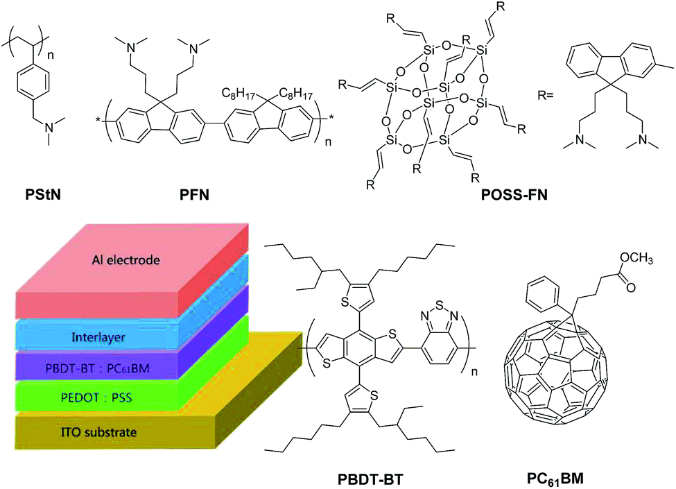 | ||
| Fig. 1 Molecular structures of the compounds studied in this work and schematic drawing of the conventional OSCs device structure. | ||
2. Experimental section
2.1 Materials
All chemicals were purchased from Sigma Aldrich. PBDT-BT was made in Flexible electronics laboratory of CSIRO Materials Science and Engineering, PC61BM was purchased from Nano-C Inc. The PFN was synthesized in accordance with literature method,37 Gel Permeation Chromatography (GPC) analysis showed the weight-average molecular weight (Mw) and polydispersity of PFN are 11796 and 1.37 respectively. The PStN was synthesized in accordance with literature method,30 GPC analysis showed the weight-average molecular weight (Mw) and polydispersity of PStN are 19300 and 1.24, respectively. The synthesis of the material POSS-FN is illustrated in Scheme S1 and described in the ESI.†33,34
2.2 Device fabrication
The device structure was ITO substrate/PEDOT:PSS (38 nm)/PBDT-BT:PC61BM (90 nm)/with or without interlayer/Al (100 nm). ITO-coated glass substrates (Lumtec 5 Ω sq−1) were cleaned sequentially with detergent aqueous solution (5% detergent aqueous solution from Daraclean® 259), deionized water, acetone and isopropyl alcohol respectively. The cleaned substrates were then exposed to UV–ozone (Novascan PDS-UVT) at 30 °C for 10 min. PEDOT:PSS (HC Starck, Baytron PAl 4083) was filtered through a 0.2 μm PTFE syringe filter and spin-coated (5000 rpm for 20 s) on the treated ITO substrates, and then annealed at 150 °C for 10 min in air. The PEDOT:PSS coated substrates at 1900 rpm for 50 s inside a nitrogen glove box. After that, the PBDT-BT:PC61BM (1:1.5 ratio by weight, and the concentration of PBDT-BT was 13 mg mL−1) blend active layer film was spin-coated from its chlorobenzene solution. Then the interlayer solutions were spin-coated on top of the active layers at 3000 rpm for 30 s. Finally, the devices were completed after deposition of 100 nm Al (Kurt J. Lesker) as the electrode in a vacuum evaporator (Angstrom Engineering Inc.) equipped with a variety of masks and a gradient shutter at a pressure below 2 × 10⁻⁶ Pa. The shadow masks gave the OSCs device areas of 0.10 cm2. The thickness of the active layer was measured with Dektak 6M Stylus Profiler (Veeco Inc.).
2.3 Measurements of J–V characteristics
Current density–voltage (J–V) characteristics of the devices were measured with an Oriel solar simulator fitted with a 1000 W Xe lamp filtered to give an output of 1000 W m−2 at AM 1.5 G. The Xenon lamp was calibrated using a standard filtered silicon reference cell (Peccell Limited Inc.). The devices were tested using a Keithley 2400 Source meter controlled by a Labview software.2.4 Other characterization methods
1H and 13C NMR spectra were recorded on a Bruker AV-400X spectrometer operating at 400 and 100 MHz respectively. Molecular weights of the polymers were measured by Gel Permeation Chromatography (GPC) using a Waters 2695 Separations Module, with a Waters 2414 Refractive Index Detector and a Waters 2996 Photodiode Array Detector, a series of four Polymer Laboratories PL Gel columns (3 × 5 μm Mixed-C and 1 × 3 μm Mixed-E), and Empower Pro Software. The molecular weights were calibrated with narrow polydispersity polystyrene standards (Polymer Laboratories Easi Cal, MW from 264 to 256000), and molecular weights are reported as polystyrene equivalents based on the refractive index detector using THF as the eluent at a rate of 1.0 mL min−1 at 30 °C. Recycling preparative GPC was performed in chloroform (3.5 mL min−1) at room temperature using a JAI LC-9201 separation module, a RI-50 s refractive index detector, a UV-3740 single wavelength detector, and a series of JAI preparative column (JAIGEL-2H 20 × 600 mm column and JAIGEL-2.5H 20 × 600 mm column).
The surface potentials of surfaces were measured on an SKP5050 Kelvin probe system (KP Technology) in air. SKPM provides the contact potential difference (CPD) between the probe tip and the surface, which for a conductive film is related to a relative difference of the work functions. The work functions were achieved from the average value of 200 points for each sample. The roughness analysis and atomic force microscopy (AFM) images were carried out on a MFD-3D AFM instrument in AC mode with a NSC15/AIBS Si cantilever (resonant frequency around 325 kHz from μ-masch). The contact angles were measured through the sessile drop goniometry method with a CAM 200 (KSV Instrument LID), and the photos were taken with a BASLER A602f-2 camera. The interfacial thermodynamics between the BHJ components and the interlayers were calculated from the Young–Dupre formulism38,39 and consequently the Good–Girifalco–Fowkers rule40 (see ESI† for details).
3. Results and discussion
The device structure of the OSCs and the chemical structures of materials used in this work are presented in Fig. 1. We used PBDT-BT35,36 as the donor and PC61BM as the acceptor. Thereinto, the weight-average molecular weight and polydispersity of PBDT-BT are 62.0 kDa and 2.31, respectively.In Fig. 2a we compare the performance of OSCs with a device structure consisting of ITO substrate/PEDOT:PSS (38 nm)/PBDT-BT:PC61BM (90 nm)/with or without interlayer/Al (100 nm) under 1000 W m−2 AM 1.5 illumination. The electrical characteristics of the devices are summarized in Table 1. Compared to the control device without interlayers, each interlayer was found to increase open circuit voltage (Voc), fill factor (FF) and PCE. This translated to a PCE increasing from 4.7% up to ∼6.4% with the various interlayers. In addition to these measurements, the series resistance and shunt resistance values were calculated from the J–V curves at dark (Fig. 2b) and are also included in Table 1. It can be seen that these devices that utilize the interlayers exhibit a decreased series resistance (Rs) from 26.8 Ω cm2 to 1.22–1.76 Ω cm2 and an increased shunt resistance (Rsh) from 70.9 kΩ cm2 to 94.1–98.7 kΩ cm2 compared to the control device without interlayer. Those device performances were obtained at optimized concentrations for spin casting PFN, POSS-FN and PStN solutions at 0.2 mg mL−1, 0.2 mg mL−1 and 0.05 mg mL−1, respectively. While the device performance depends on the interlayer thickness, the variation is much smaller for PFN (solution at 1.0 mg mL−1, PCE = 5.00%; solution at 0.2 mg mL−1, PCE = 6.13%) than POSS-FN (solution at 1.0 mg mL−1, PCE = 4.07%; solution at 0.2 mg mL−1, PCE = 6.17%) and PStN (solution at 1.0 mg mL−1, PCE = 1.68%; solution at 0.05 mg mL−1, PCE = 6.10%) as the spin concentration increased (see Fig. S3–S5 and Tables S1–S3 in the ESI†). When the highest concentration of 1.0 mg mL−1 solutions was used, Rs increased significantly with insulating PStN and POSS-FN, while that with PFN increased only slightly. We note that a very dilute solution at 0.05 mg mL−1 was used for PStN to obtain the optimized device performance. With this very thin interlayer, the insulating nature of the material is not an issue as electrons can readily tunnel through the presented electrical barrier.11,12,41 These collective results demonstrate that both the linear materials and the three-dimensional material are beneficial for solar cell performance and they are quite similar when they were used as surface modifiers, despite of the various molecular structures.
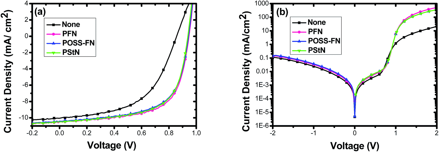 | ||
| Fig. 2 Device performances for various interfacial treatments as indicated. Current density–voltage curves of the OSCs based on PBDT-BT/PC61BM (1:1.5 w/w) with or without interlayer under the illumination of AM 1.5 G, 1000 W m−2 (a) and under dark (b). | ||
| Interlayer | Voc [V] | Jsc [mA cm−2] | FF [%] | PCE [%] Max | PCE [%] Min | Average PCE [%] [5 devices] | Standard derivation | Rs [Ω cm2] | Rsh [kΩ cm2] |
|---|---|---|---|---|---|---|---|---|---|
| None | 0.86 ± 0.01 | 10.2 ± 0.2 | 53.7 ± 0.3 | 4.70 | 4.47 | 4.6 ± 0.1 | 0.19 ± 0.01 | 26.8 ± 0.2 | 70.9 ± 0.2 |
| POSS-FN | 0.94 ± 0.01 | 10.4 ± 0.2 | 64.4 ± 0.2 | 6.27 | 6.01 | 6.1 ± 0.1 | 0.15 ± 0.01 | 1.5 ± 0.1 | 95.9 ± 0.1 |
| PFN | 0.95 ± 0.01 | 10.5 ± 0.2 | 64.2 ± 0.2 | 6.40 | 6.09 | 6.2 ± 0.1 | 0.16 ± 0.01 | 1.3 ± 0.1 | 96.6 ± 0.1 |
| PStN | 0.94 ± 0.01 | 10.5 ± 0.3 | 63.2 ± 0.3 | 6.25 | 6.03 | 6.1 ± 0.2 | 0.21 ± 0.01 | 1.6 ± 0.1 | 95.1 ± 0.1 |
The morphology and surface roughness of the films with the various interlayers were investigated by atomic force microscopy (AFM) (see Fig. S6 in the ESI†). The pristine PBDT-BT:PC61BM film shows surface root mean square (RMS) of 1.87 nm. After incorporating the PFN interlayer, a similar film roughness of 1.61 nm was noted. In contrast, the presence of the three-dimensional interlayer POSS-FN induced a roughening of the surface topography, with the RMS increasing to 6.71 nm. Similarly, we found a RMS increase to 5.92 nm for another linear interlayer PStN.
The surface potential is a sensitive pointer to the extent of surface traps, charge density, natures of chemical bonds and so on of a given interface.42 The SKPM results are displayed in Table 2. Each value was calculated relative to ITO, which was set at a nominal value of 4.70 eV.42,43 The work function of PBDT-BT:PC61BM active layer characterized from SKPM is 4.68 eV. The interlayers were found to reduce this work function to 4.19 eV (PFN), 4.42 eV (POSS-FN) and 4.25 eV (PStN), indicating various degrees of interfacial dipole formation. Previously, a hyper-branched version of PFN, HBPFN, was reported to only slightly reduce the work function of another typical active layer (containing PBDTTT-C-T and PCBM), from 4.50 eV to 4.45 eV,30 similar to the case with the hybrid material POSS-FN here. These two three dimensional interfacial materials, HBPFN and POSS-FN, both show relatively weaker interfacial dipole formation between the active and the interlayer materials than the linear ones PFN and PStN.
For the interfaces between the interfacial material and the ITO electrode, similar changes to the work function of between −0.3 and −0.5 eV were observed. Again, we found that linear interlayer materials PFN and PStN form slightly larger work function reduction on ITO than the three-dimensional materials POSS-FN and HBPFN.30 In comparison, larger dipoles have been reported between amines and metals, including gold and aluminium.29 These are likely to originate from chelation of the metal surface by the lone electron pair on the nitrogen and the accompanying interfacial polarization effects.44–46 Indeed, SKPM measurements on freshly evaporated gold coated by our interlayers presented dipole shifts of −0.6 up to −0.7 eV, regardless of the chemical and physical (linear or three dimensional) structures of the interlayers. Similar to the gold interface, comparable interfacial dipoles are expected for the interfaces between the interlayer materials and the evaporated aluminium electrode. However, the rapid oxidation of the aluminium surface prevented us from attaining a reliable estimate of the electrical structure using SKPM. In any case, by assuming the dipole formation at the top Al interface and taking ∼4.3 eV as its nominal work function, we can approximate the schematic energy level diagram of the components within our conventionally architectured devices (Fig. 3). The above results suggest the importance of two interfaces: (i) the interlayer and the active blend layer; and (ii) the interlayer and the Al cathode. Based on these results, we hypothesize that the active layer–interlayer interface causes a relatively small, but unfavourable work function modification. The latter interface, which is dominated by the strong chelation of the metal surface by amine groups, acts to lower the work function significantly at the cathode interface to a sufficient level where it provides ohmic contact for all the interlayer materials. As a result, a lower interfacial trap density and maximization of the electric field across the device would be expected.
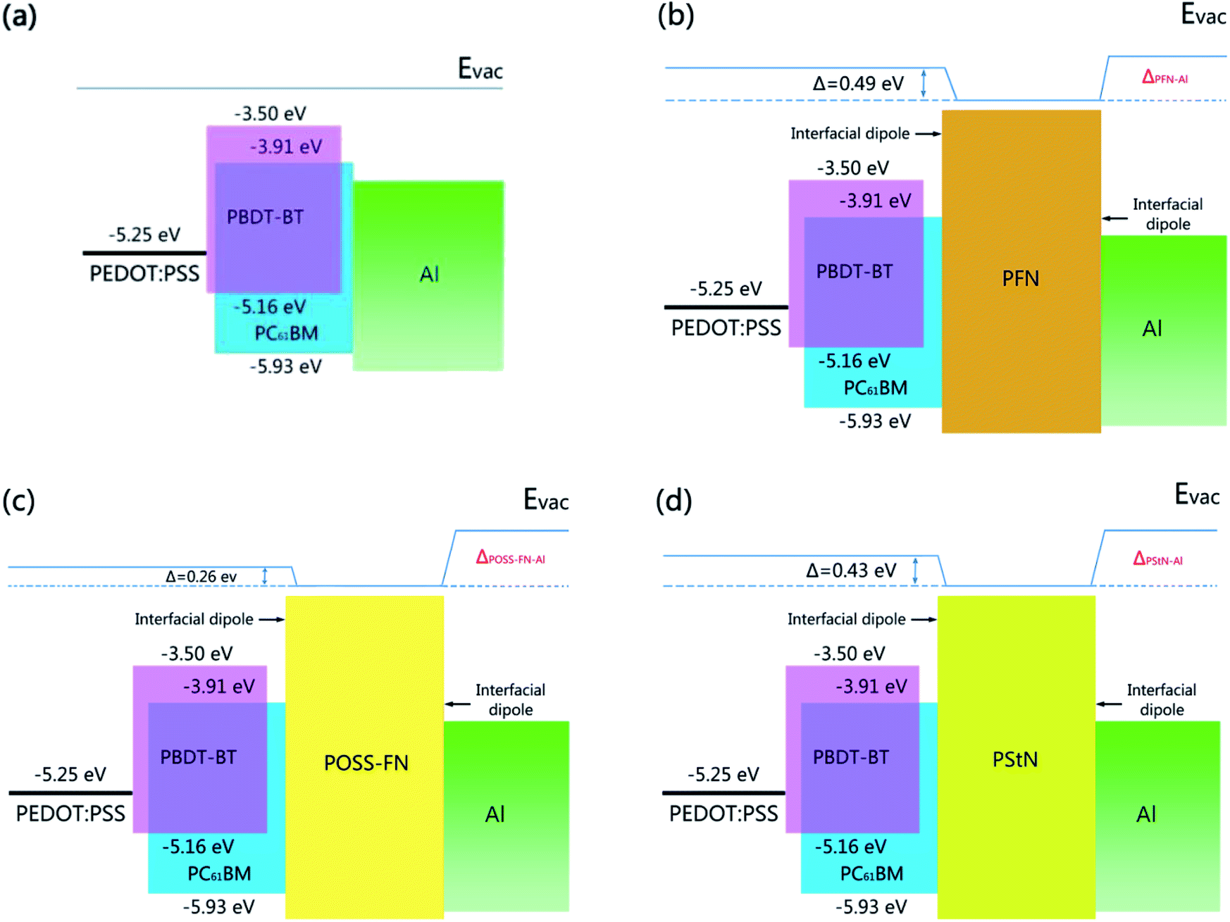 | ||
| Fig. 3 Schematic energy levels of the devices with various interfacial treatments: (a) none, (b) PFN, (c) POSS-FN, (d) PStN. | ||
The above results clearly show that the molecular architecture has clear effect on the dipole formation. The three-dimensional materials form weak interfacial dipole with active layer than linear materials. However, they form similar interfacial dipoles with the cathode, which are more critical and significant to the device performance improvement, so all the studied interface materials are performed similarly in the devices.
Besides the dramatic enhancement in Voc, stemming from interfacial dipole formation, the enhancement of the FF by 20% is suggestive of significant improvements to the charge transport properties. To explore their origins, the charge transport mobilities were approximated using a space charge limited current (SCLC) model by single-carrier devices.47 The structures for electron-only and hole-only devices were: ITO substrate/TIPD (12 nm)/PBDT-BT:PC61BM (90 nm)/with or without interlayer/Al (100 nm) and ITO substrate/PEDOT:PSS (38 nm)/PBDT-BT:PC61BM (90 nm)/with or without interlayer/MoO3 (8 nm)/Au (40 nm), respectively. Here TIPD represents a titanium chelate which was used for the electron collection layer.48 The charge transport mobilities were obtained as field independent values in Table 3 (J–V characteristics and corresponding fitting results from SCLC model of hole-only and electron-only devices are in Fig. S7 and S8 respectively in the ESI†). For pristine PDBT-BT-PC61BM devices, the hole mobility of 1.65 × 10⁻⁵ cm2 V−1 s−1 is almost one order of magnitude lower than the electron mobility of 1.54 × 10⁻⁴ cm2 V−1 s−1. After incorporating the interlayers, the electron mobility remained similar to that of the pristine device, whereas the hole mobilities all increased to ∼1 × 10⁻⁴ cm2 V−1 s−1, almost one order of magnitude higher. This more balanced charge transport regime could explain the higher FF in the devices based on the well-known fact that it restricts the build-up of space charge, which consequently reduces the extent of charge recombination in devices.11,12,41 Similar results were reported in literature.11,12,49,50
| Interlayer | Electron mobilitya [cm2 V−1 s−1] | Hole mobilityb [cm2 V−1 s−1] |
|---|---|---|
| a Electron-only device: ITO/TIPD (12 nm)/PBDT-BT:PC61BM (90 nm)/with or without interlayer/Al (100 nm).b Hole-only device: ITO/PEDOT:PSS (38 nm)/PBDT-BT:PC61BM (90 nm)/with or without interlayer/MoOx (8 nm)/Au (40 nm). | ||
| None | 1.81 × 10⁻⁴ | 1.65 × 10⁻⁵ |
| PFN | 2.14 × 10⁻⁴ | 1.09 × 10⁻⁴ |
| POSS-FN | 2.34 × 10⁻⁴ | 1.20 × 10⁻⁴ |
| PStN | 1.54 × 10⁻⁴ | 1.25 × 10⁻⁴ |
In addition to the changes of the morphology, work function and charge transport mobility, the thermodynamics at the surface was also studied.51 The results of interfacial thermodynamics (Table 4) show that the modification of the BHJ surface by all the interlayers causes a slight increase of the surface energy γ from 27.1 to 27.9–29.7 mN m−1, and an obvious increase in the electron donor contributions γ− from 1.83 to 3.1–15.1 mN m−1. This increase in the basic component at the surface is suggestive of tertiary amine groups being exposed at the surface, thus favourably contributing to the interfacial dipole that is formed within these thin layers. We note that the electron donor contributions γ− with linear polymers PFN and PStN interlayers are much higher than that with three-dimensional interlayer POSS-FN. The correlation of the electron donor contribution with the interfacial dipole could be a topic for future work.
| PBDT-BT:PC61BM | PBDT-BT:PC61BM/PFN | PBDT-BT:PC61BM/POSS-FN | PBDT-BT:PC61BM/PStN | ||
|---|---|---|---|---|---|
| Contact angle | Water | 96° ± 2° | 76° ± 3° | 88° ± 1° | 77° ± 1° |
| Ethylene glycol | 72° ± 1° | 64° ± 3° | 60° ± 2° | 59° ± 1° | |
| Hexadecane | 16° ± 1° | 16° ± 1° | 17° ± 1° | 17° ± 1° | |
| Calculated surface energy component [mN m−1] | γ | 27.10 | 27.89 | 29.22 | 29.70 |
| γLW | 26.38 | 26.33 | 26.25 | 26.27 | |
| γAB | 0.72 | 1.56 | 2.97 | 3.43 | |
| γ+ | 0.07 | 0.04 | 0.72 | 0.24 | |
| γ− | 1.83 | 15.14 | 3.06 | 12.25 | |
| Interfacial surface tension [mJ m−2] | — | −0.33 | 0.46 | 0.97 | |
| Interfacial free energy [mJ m−2] | — | −55.31 | −55.85 | −55.83 | |
4. Conclusions
We have studied an alcohol soluble hybrid organic–inorganic three-dimensional material and used it as interfacial layers at the cathode of organic bulk heterojunction solar cells. Meanwhile, various alcohol-soluble linear polymers, including the semi-conductive PFN and an insulating PStN are studied as a contrast in the same system. Compared to devices made without these interlayers and using a typical aluminium cathode, all interlayer materials exhibited improved PCE, Voc, Jsc and FF device characteristics, with remarkably similar values.Our results show two interfaces for the interfacial dipoles formation have to be considered: one between the interlayer and the active blend is slightly stronger for linear polymers than the three-dimensional materials, and they are unfavourable and not determined to the device performance, and the other between the interlayer and the metal cathode is significant and favourable for the device performance improvement. In latter case, we found very similar effect for linear and three-dimensional materials, and thus the device performances are improved similarly. The difference and similarity between three-dimensional and linear materials in this study implies that the molecular architecture needs further study to help understanding the interfaces, which could help the development and design of new interface materials. Besides, high bandgap interfacial materials such as POSS-FN and PStN could have some advantages in other applications, such as organic light emitting diodes, where low energy traps or injection barrier are concerned.
Acknowledgements
We acknowledge financial support through CSIRO-CAS joint project on “Nanotechnology and novel energy materials” focus area and scholarship from Chinese Scholarship Council for Dr M. L. Lv. This work was funded through the Flexible Electronics Theme of the CSIRO Manufacturing Flagship, National Natural Science Foundation of China (Grant No. 21502033), Science and Technology Cooperation Program of Guizhou, China (Grant No. QKHLH[2015]7094). Support from the Victorian Organic Solar Cell Consortium (Victorian Department of Primary Industries, Sustainable Energy Research and Development Grant and Victorian Department of Business and the Australian Solar Institute) is acknowledged. J. Jasieniak acknowledges financial support through the Australian Research Council grant DP110105341. Dr Ming Chen helped the synthesis of PBDT-BT.Notes and references
- G. Yu, J. Gao, J. C Hummelen, F. Wudl and A. J. Heeger, Science, 1995, 270, 1789 CAS.
- R. Steim, F. R. Kogler and C. J. Brabec, J. Mater. Chem., 2010, 20, 2499 RSC.
- S. H. Liao, H. J. Jhuo, P. N. Yeh, Y. S. Cheng, Y. L. Li, Y. H. Lee, S. Sharma and S. A. Chen, Sci. Rep., 2014, 24, 6813 Search PubMed.
- W. C. Zhao, D. P. Qian, S. Q. Zhang, S. S. Li, I. Olle, F. Gao and J. H. Hou, Adv. Mater., 2016, 28, 4734–4739 CrossRef CAS PubMed.
- W. C. Zhao, S. Q. Zhang and J. H. Hou, Sci. China: Chem., 2016, 12, 1–9 Search PubMed.
- S. S. Li, L. Ye, W. C. Zhao, S. Q. Zhang, M. Subhrangsu, A. Harald and J. H. Hou, Adv. Mater., 2016, 28, 9423–9428 CrossRef CAS PubMed.
- Z. G. Yin, J. J. Wei and Q. D. Zheng, Adv. Sci., 2016, 3, 1500362 CrossRef PubMed.
- C. C. Chueh, C. Z. Li and A. K.-Y. Jen, Energy Environ. Sci., 2015, 8, 1160–1189 CAS.
- Z. He, C. Zhang, X. Xu, L. Zhang, L. Huang, J. W. Chen, H. B. Wu and Y. Cao, Adv. Mater., 2011, 23, 3086 CrossRef CAS PubMed.
- H. Zheng, Y. Zheng, N. Liu, N. Ai, Q. Wang, S. Wu, J. Zhou, D. Hu, S. Yu, S. Han, W. Xu, C. Luo, Y. Meng, Z. Jiang, Y. Chen, D. Li, F. Huang, J. Wang, J. Peng and Y. Cao, Nat. Commun., 2013, 4, 1971–1977 Search PubMed.
- Z. C. He, C. M. Zhong, X. Huang, W. Wong, H. B. Wu, L. W. Chen, S. J. Su and Y. Cao, Adv. Mater., 2011, 23, 4636 CrossRef CAS PubMed.
- Z. C. He, C. M. Zhong, S. J. Su, M. Xu, H. B Wu and Y. Cao, Nat. Photonics, 2012, 6, 591 Search PubMed.
- Y. Liu, J. Zhao, Z. Li, C. Mu, W. Ma, H. Hu, K. Jiang, H. Lin, H. Ade and H. Yan, Nat. Commun., 2014, 5, 5293 CrossRef CAS PubMed.
- G. Kim, J. Kong, J. Kim, H. Kang, H. Back, H. Kim and K. Lee, Adv. Energy Mater., 2015, 5, 1401298 CrossRef.
- S. H. Liao, H. J. Jhou, Y. S. Cheng and S. A. Chen, Adv. Mater., 2013, 25, 4766 CrossRef CAS PubMed.
- Z. G. Yin, Q. D. Zheng, S. C. Chen, D. D. Cai and Y. L. Ma, Adv. Energy Mater., 2016, 5, 1501493 CrossRef.
- Z. G. Yin, Q. D. Zheng, S. C. Chen, J. X. Li, D. D. Cai, Y. L. Ma and J. J. Wei, Nano Res., 2015, 8, 456–468 CrossRef CAS.
- T. Yang, M. Wang, C. Duan, X. Hu, L. Huang, J. Peng, F. Huang and X. Gong, Energy Environ. Sci., 2012, 5, 8208 CAS.
- Y. Chen, Z. T. Jiang, M. Gao, S. E. Watkins, P. Lu, H. Q. Wang and X. W. Chen, Appl. Phys. Lett., 2012, 100, 203304 CrossRef.
- S. H. Liao, Y. L. Li, T. H. Jen, Y. S. Cheng and S. A. Chen, J. Am. Chem. Soc., 2012, 134, 14271 CrossRef CAS PubMed.
- K. M. O'Malley, C. Z. Li, H. L. Yip and A. K. Y. Jen, Adv. Energy Mater., 2012, 2, 82 CrossRef.
- C. Z. Li, C. C. Chueh, H. L. Yip, F. Ding, X. Li and A. K. Y. Jen, Adv. Mater., 2013, 25, 2457 CrossRef CAS PubMed.
- D. Hong, M. L. Lv, M. Lei, Y. Chen, P. Lu, Y. G. Wang, J. Zhu, H. Q. Wang, M. Gao, S. E. Watkins and X. W. Chen, ACS Appl. Mater. Interfaces, 2013, 5, 10995–11003 CAS.
- S. S. Li, M. Lei, M. L. Lv, S. E. Watkins, Z. A. Tan, J. Zhu, J. H. Hou, X. W. Chen and Y. F. Li, Adv. Energy Mater., 2013, 23, 1569–1574 CrossRef.
- T. Cao, Z. W. Wang, Y. J. Xia, B. Song, Y. Zhou, N. Chen and Y. F. Li, ACS Appl. Mater. Interfaces, 2016, 8, 18284–18291 CAS.
- X. R. Jia, L. P. Zhang, Q. Luo, H. Lu, X. Y. Li, Z. Z. Xie, Y. Z. Yang, Y. Q. Li, X. G. Liu and C. Q. Ma, ACS Appl. Mater. Interfaces, 2016, 8, 18410–18417 CAS.
- Y. H. Zhou and B. Kippelen, Science, 2012, 336, 327 CrossRef CAS PubMed.
- Y. H. Zhou, C. Fuentes-Hernandez, J. W. Shim, T. M. Khan and B. Kippelen, Energy Environ. Sci., 2012, 5, 9827 CAS.
- H. Kang, S. Hong, J. Lee and K. Lee, Adv. Mater., 2012, 24, 3005 CrossRef CAS PubMed.
- M. L. Lv, S. S. Li, J. J. Jasieniak, J. H. Hou, J. Zhu, Z. A. Tan, S. E. Watkins, Y. F. Li and X. W. Chen, Adv. Mater., 2013, 23, 6889–6894 CrossRef PubMed.
- W. D. Xu, Z. P. Kan, T. L. Ye, L. Zhao, W. Y. Lai, R. D. Xi, G. Lanzani, E. P. Keivanidis and W. Huang, ACS Appl. Mater. Interfaces, 2015, 7, 452–459 CAS.
- Y. Zou, Z. C. He, B. F. Zhao, Y. Liu, C. L. Yang, H. B. Wu and Y. Cao, Sci. Rep., 2015, 5, 17329 CrossRef CAS PubMed.
- K. Y. Pu, K. Li and B. Liu, Adv. Mater., 2010, 22, 643–646 CrossRef CAS PubMed.
- K. Y. Pu, K. Li, X. H. Zhang and B. Liu, Adv. Mater., 2010, 22, 4186–4189 CrossRef CAS PubMed.
- J. Subbiah, B. Purushothaman, M. Chen, T. S. Qin, M. Gao, D. Vak, F. H. Scholes, X. W. Chen, S. E. Watkins, G. J. Wilson, A. B. Holmes, W. W. H. Wong and D. J. Jones, Adv. Mater., 2015, 27, 702–705 CrossRef CAS PubMed.
- M. Gao, J. Subbiah, P. B. Geraghty, M. Chen, B. Purushothaman, X. W. Chen, T. S. Qin, D. Vak, F. H. Scholes, S. E. Watkins, M. Skidmore, G. J. Wilson, A. B. Holmes, D. J. Jones and W. W. H. Wong, Chem. Mater., 2016, 28, 3481–3487 CrossRef CAS.
- F. Huang, H. B. Wu, D. L. Wang, W. Yang and Y. Cao, Chem. Mater., 2004, 16, 708–716 CrossRef CAS.
- X. J. Wang, T. Ederth and O. Inganäs, Langmuir, 2006, 22, 9287–9294 CrossRef CAS PubMed.
- L. M. Lander, L. M. Siewieerski, W. J. Brittain and E. A. Vogler, Langmuir, 1993, 9, 2237–2239 CrossRef CAS.
- H. K. Nguyen, M. Labardi, S. Capaccioli, M. Lucchesi, P. Rolla and D. Prevosto, Macromolecules, 2012, 45, 2138–2144 CrossRef CAS.
- K. Zhang, X. Guan, F. Huang and Y. Cao, Acta Chim. Sin., 2012, 70, 2489 CrossRef CAS.
- J. S. Kim, B. Lägel, E. Moons, N. Johansson, I. D. Baikie, W. R. Salaneck, R. H. Friend and F. Cacialli, Synth. Met., 2000, 111–112, 311–314 CrossRef CAS.
- R. J. Davis, M. T. Lloyd, S. R. Ferreira, M. J. Bruzek, S. E Watkins, L. Lindell, P. Sehati, M. Fahlman, J. E. Anthony and J. W. P. Hsu, J. Mater. Chem., 2011, 21, 1721 RSC.
- A. Grubisic, X. Li, G. Gantefoer, K. H. Bowen, H. Schnöckel, F. J. Tenorio and A. Martinez, J. Chem. Phys., 2009, 131, 184305 CrossRef PubMed.
- D. Y. Wu, D. Y. Hayashi, C. H. Chang, K. K. Liang and S. H Lin, J. Chem. Phys., 2003, 118, 4073 CrossRef CAS.
- A. Martínez, Chem. Soc., 2005, 16, 337–344 Search PubMed.
- P. W. M. Blom and M. C. J. M. Vissenberg, Mater. Sci. Eng., 2000, 27, 53 Search PubMed.
- Z. A. Tan, W. Zhang, Z. Zhang, D. Qian, Y. Huang, J. H. Hou and Y. F. Li, Adv. Mater., 2012, 24, 1476 CrossRef CAS PubMed.
- H. Q. Zhou, Y. Zhang, J. Seifter, S. D. Collins, C. Luo, G. C. Bazan, T. Q. Nguyen and A. J. Heeger, Adv. Mater., 2013, 25, 1646–1652 CrossRef CAS PubMed.
- A. J. Heeger, G. C. Bazan, T. Q. Nguyen and F. Wudl, Technical Report, 2015 Search PubMed.
- M. D. Clark, M. L. Jespersen, R. J. Patel and B. J. Leever, ACS Appl. Mater. Interfaces, 2013, 5, 4799–4807 CAS.
Footnote |
| † Electronic supplementary information (ESI) available: The detailed information of Experimental section. Scheme S1: synthesis route of POSS-FN; Fig. S1: (a)1H NMR; (b) 13C NMR in CDCl3 spectra of compound 2; Fig. S2: (a)1H NMR in MeOD; (b) 13C NMR in CDCl3 spectra of POSS-FN; Fig. S3: J–V curves of devices with PFN interlayer spin casted from methanol solutions; Fig. S4: J–V curves of devices with POSS-FN interlayer spin casted from methanol solutions; Fig. S5: J–V curves of devices with PStN interlayer spin casted from methanol solutions; Fig. S6: AFM (5 × 5 μm, scan rate is 0.86 Hz) images of blend films without interlayer (a), with PFN (b), with POSS-FN (c), with PStN (d); Fig. S7: current density versus applied voltage (J–V) characteristics and corresponding fitting results from SCLC model of hole-only devices ITO substrate/PEDOT:PSS (38 nm)/PBDT-BT:PC61BM (90 nm)/with or without interlayer/MoOx (8 nm)/Au (40 nm): without interlayer (a), with PFN interlayer (b), with POSS-FN interlayer (c) and with PStN interlayer (d); Fig. S8: current density versus applied voltage (J–V) characteristics and corresponding fitting results from SCLC model of electron-only devices ITO substrate/TIPD (12 nm)/PBDT-BT:PC61BM (90 nm)/with or without interlayer/Al (100 nm): without interlayer (a), with PFN interlayer (b), with POSS-FN interlayer (c) and with PStN interlayer (d); Fig. S9: contact angle images. See DOI: 10.1039/c7ra04044j |
| This journal is © The Royal Society of Chemistry 2017 |