DOI:
10.1039/C7RA04018K
(Paper)
RSC Adv., 2017,
7, 26776-26782
Insights into the role of the interface defects density and the bandgap of the back surface field for efficient p-type silicon heterojunction solar cells†
Received
9th April 2017
, Accepted 14th May 2017
First published on 19th May 2017
Abstract
An n-type silicon wafer appears to be an excellent base material for high efficiency silicon heterojunction solar cells with high annual energy output. The further development of viable p-wafer cells would open many industrial photovoltaic options. Here, the role of the interface defects density and the bandgap of the back surface field of p-type silicon heterojunction solar cells have been investigated in detail to provide guidelines for achieving high performance. The result indicates that the output characteristics of the heterojunction solar cells are sensitive to the density of interface defects (Dit) at both sides of the c-Si surface. However, the output parameters primarily affected by Dit at the front and rear side are not identical. Back surface field (BSF), which aims to reduce photo-generated carriers' recombination at the rear interface, has also been optimized by adjusting the bandgap to improve the collection efficiency. Finally, based on experimental results, we propose that the conversion efficiency of p-type silicon heterojunction solar cells could be increased beyond 23% by efficiently regulating the bifacial Dit and the bandgap of the BSF layer.
1. Introduction
Silicon heterojunction (SHJ) solar cells constructed with ultrathin hydrogenated amorphous silicon (a-Si:H) on a crystalline silicon (c-Si) absorber layer are promising candidates for high-efficiency, low-cost solar cells. Compared with traditional monocrystalline silicon solar cells, SHJ solar cells generally exhibit higher open-circuit voltages (Voc) because wide-band-gap a-Si:H is used as the emitter layer and the metal contact is separated from the wafer by a-Si:H films and indium tin oxide (ITO), which reduces the amount of interface recombination.1–3 Moreover, SHJ solar cells could be fabricated with low-temperature or photolithographic-free processes, since passivation of the c-Si wafer surfaces and formation of the emitter and back surface field (BSF) are all performed with thin intrinsic and doped a-Si:H layers, usually deposited by low-temperature plasma-enhanced chemical vapor deposition.4,5
So far, the highest efficiency silicon heterojunction solar cells were obtained using n-doped, rather than p-doped, c-Si wafers.6 However, n-type wafers are still less readily available on the market than p-type wafers, which are widely used for the production of conventional (diffused-emitter) silicon solar cells. The possibility to produce high-efficiency heterojunction solar cells from p-type wafers is, thus, of great practical interest. The p-type SHJ solar cells have already been demonstrated by several groups but with efficiencies significantly lower than those achieved on n-type wafers.3,5,6 For p-type silicon heterojunction solar cells, the performance is also more sensitive to the density of a-Si:H/c-Si interface defects, not only because the p–n junction is across two different materials, but also owing to the asymmetry between the conduction and valence band offsets.7 Yet up to now, there still have unified understanding about the different influences caused by the Dit at the front and rear sides of the p-type SHJ solar cells. Thus, it is necessary to understand the role of the Dit and the bandgap alignment for p-type SHJ solar cells in order to further improve the performance and accelerating its practical application.
Numerical analysis describe the basic phenomena present in photovoltaic devices, allowing intuitive examination of each parameter in solar cells and thus identifying the optimal conditions for operating. In this work, we make an insight into the relationship of the Dit at the front and rear sides of the crystalline silicon by an extended Shockley–Read–Hall formalism.8 Our results present that the Dit at front side is primarily affected the Voc of the p-type SHJ solar cells, while the Dit at the rear side could act upon the FF and Jsc of the device. Also, in order to achieve a good function of photo-generated carriers' collection, the bandgap of the BSF should be adjusted in the range of 1.7–1.8 eV to achieve the efficiency more than 23%.
2. Numerical modeling
In order to give an accurately insight into the sensitive parameters for p-type SHJ solar cells, analytical calculations are unavoidable tool to model the behavior of a full cell architecture especially under equilibrium conditions. The Poisson and the continuity equations for electrons and holes are solved considering Shockley–Read–Hall recombination statistics for the a-Si:H and for the defect layer at the interface between a-Si:H and c-Si. In practical manufacturing process, Dit can be suppressed by wet chemical cleaning of the c-Si surface followed by H-terminated and the growth of a-Si:H, which saturates the silicon dangling bonds with atomic hydrogen.9–11 Garín et al.12 suggested that the Shockley–Read–Hall formalism, which has been widely used to depict c-Si surface passivation schemes by SiO2 and a-SiNx:H, can model the i-a-Si:H/c-Si interface recombination, in which the i-a-Si:H thin film dangling bond states in the proximity of abrupt i-a-Si:H/c-Si interface can be considered to be an effective interface and included in Dit. Nevertheless, the charge effect of doped a-Si:H layer defects on the interface recombination was eliminated, and Dit was oversimplified by a single level defect state at mid-gap. Shu et al.13 extend the Shockley–Read–Hall approach to more accurately model the interface recombination through a continuously distributed Dit, with the effect of doped a-Si:H defect states also taken into account. Herein, we further extend this comprehensive Shockley–Read–Hall model in this work by inducing a defect layer to describe injection level dependent surface recombination velocity (Sit).
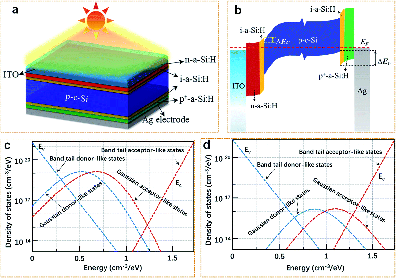
The complete architecture of ITO/n-a-Si:H/i-a-Si:H/p-c-Si/i-a-Si:H/p+-a-Si:H/Ag and corresponding bandgap schematic diagram in this numerical analysis are exhibited in Fig. 1a and b. We performed numerical simulations of p-type SHJ solar cells with efficient tool named AFORS-HET.14 The basic parameters in this numerical modeling, which extract from different state-of-the-art SHJ solar cells experimental results,6,15–18 are shown as Table 1. The absorber of the solar cell is standard 300 μm thick p-type c-Si, with an acceptor density of 1.5 × 1016 cm−3. It is characterized by a single donor-type defect centered at mid-gap with a density of 1010 cm−3 and the capture cross section for holes and for electrons is equal to 10−14 cm2. The density of states of the n-a-Si:H emitter layer and i-a-Si:H passivation layer, including two Gaussian distributions of deep defects and the valence and conduction band tails states are exhibited in Fig. 1c and d. An 80 nm ITO is used to be the transparent conductive oxide layer and a thin c-Si layer (3 nm) with average distribution continuous donor and acceptor defect states in the band gap has been inserted between the i-a-Si:H and c-Si to substitute the interface defects. The density of interface defects translates into a volume defects density by:
| | |
d × S × ρvolume = S × ρinterface
| (1) |
where
d is the thickness of the volume defects layer,
S is the surface area of the c-Si,
ρvolume and
ρinterface are the defect states density at the volume and surface of c-Si respectively. The surface recombination velocities of the electrons and holes are both set to 1.0 × 10
7 cm s
−1. The solar AM1.5 radiations are adopted as the illuminating source with the power density of 100 mW cm
−2 and the ITO/n-a-Si:H contact is fixed as flat band in calculations.
 |
| | Fig. 1 (a) Schematic of the SHJ solar cells for numerical analysis. (b) Schematics of energy diagram of p-type SHJ solar cell at equilibrium condition. The dashed lines are Fermi energy (EF), conduction band offset (ΔEc) and valence band offset (ΔEv), respectively. Distribution of gap defects in (c) n-a-Si:H and (d) i-a-Si:H layer include two Gaussian distributions of deep defects and the band tails states of the valence band and conduction band. | |
Table 1 Main parameter values adopted for SHJ solar cells in this study
| Parameters |
a-Si:H(n) |
a-Si:H(i) |
a-Si:H(p+) |
c-Si(p) |
| Layer thickness (nm) |
10 nm |
5 nm |
5 nm |
300 μm |
| Electron affinity (eV) |
3.9 |
3.9 |
2.9 |
4.05 |
| Mobility gap (eV) |
1.80 |
1.80 |
Variable |
1.12 |
| Optical band gap (eV) |
1.72 |
1.72 |
1.72 |
1.12 |
| Effective density of states Nc/Nv (cm−3) |
1020/1020 |
1020/1020 |
1020/1020 |
2.8 × 10¹⁹/2.6 × 1019 |
| Doping concentration (cm−3) |
5 × 10²⁰ |
Nd = 100 |
9 × 10²⁰ |
1.5 × 10¹⁶ |
| Electron mobility (cm2 V−1 s) |
5 |
5 |
5 |
1041 |
| Hole mobility (cm2 V−1 s) |
1 |
1 |
1 |
412.9 |
| Standard deviation in Gaussian states (eV) |
0.21 |
0.21 |
0.21 |
— |
| Electron capture cross (cm2) |
7 × 10⁻¹⁶ |
7 × 10⁻¹⁶ |
3 × 10⁻¹⁵ |
1 × 10⁻¹⁴ |
| Hole capture cross (cm2) |
7 × 10⁻¹⁶ |
7 × 10⁻¹⁶ |
3 × 10⁻¹⁴ |
1 × 10⁻¹⁴ |
| Urbach energies Etail,V and Etail,C (eV) |
0.094/0.068 |
0.094/0.035 |
0.12/0.08 |
— |
3. Results and discussion
Role of the bifacial Dit for p-type SHJ solar cells
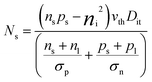
Recombination through defect levels in semiconductors is usually described by the Shockley–Read–Hall theory in this work. The surface recombination rate (Ns) of solar cells can be given by,19| |
 | (2) |
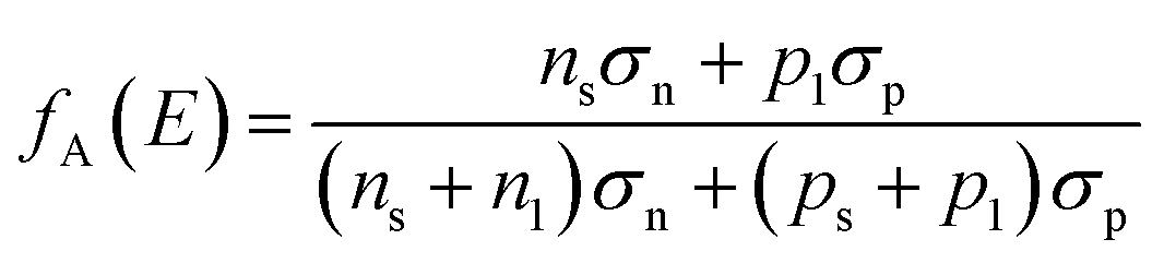
Where σn, σp and ns, ps are the capture cross-sections and concentrations of electrons and holes respectively. vth is the thermal velocity. nl and pl are the statistical factor for electrons and holes respectively. Therefore, the Sit could be given as,| |
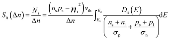 | (3) |
where Δns is the excess carrier density at the surface. For SHJ solar cells, the Voc is related to the interface recombination via:20| |
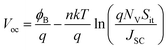 | (4) |
kT is the thermal energy, ϕB is the effective barrier, q is the elementary charge, Nv is the effective density of states in the valence band. According to eqn (3) and (4), it can be concluded that (nsps − ni2) and Dit affect the performance of the solar cells by determining the Voc. So we assumed different Dit at the front side of c-Si surface to depict the corresponding influences on device, thus providing the threshold of the Dit to maintain high performance p-type SHJ solar cells.
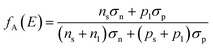
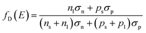
Fig. 2a shows the band diagrams with different values of Dit at the front side of the heterojunction under illumination. The interface charge (Qit) by trapping carrier is related to Dit (E) and the difference in occupancy by electrons and holes via13
| |
 | (5) |
where the
DAit(
E) and
DDit(
E) are the continuous distributed acceptor-type and donor-type
Dit(
E) within c-Si bandgap. The
fD(
E) and
fA(
E) are the occupancies of the donor and acceptor defects states, respectively, expressed by
| |
 | (6) |
| |
 | (7) |
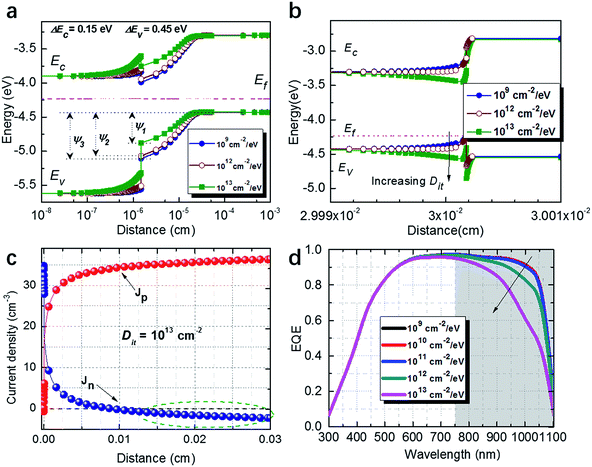 |
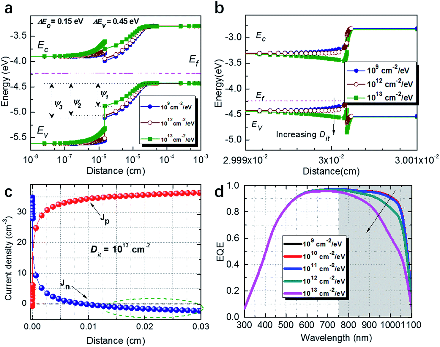
| | Fig. 2 Band diagrams and quasi-Fermi levels of the heterojunction in (a) front and (b) rear side of the p-type SHJ solar cells as the Dit increased from 109 cm−2 eV−1 to 1013 cm−2 eV−1. ψ1, ψ2, and ψ3 are the equilibrium band bending in c-Si when the Dit is 109, 1012, and 1013 cm−2 eV−1, respectively. (c) The photo-generated holes and electrons current density (Jn and Jp) as a function of position in the SHJ solar cells when the Dit at rear side is 1013cm−2 eV−1. (d) The EQE spectrum of the p-type SHJ solar cells with different Dit at rear side of c-Si. | |
Since the minority carriers in p-type are electrons, which have larger capture cross sections than holes, the high Dit will increase the number of Qit by trapping carriers. If Qit can become comparable with the charges in the a-Si:H and c-Si, and hence the bands need to realign to keep the system charge balance.21 As a result, the band bending (ψ) in c-Si is reduced (ψ1, ψ2, and ψ3 are the equilibrium band bending in c-Si when the Dit are 109, 1012, and 1013 cm−2 eV−1, respectively). Meanwhile, the recombination possibility at the a-Si:H/c-Si heterointerface will increase with the reduction of the band bending, due to the declining of the driven force in c-Si for separating photo-generated carriers.22
The influences of Dit on the rear-side heterojunction band bending have been exhibited in Fig. 2b. As described above, the number of trapped holes will be much larger than that of electrons, and thus creating positively Qit. Similar with the front side, when the magnitude of Qit can be closed to the ionized donor in the depletion region (e.g., 1013 cm−2 eV−1), c-Si energy band at rear interface even can bend downward. Fig. 2c shows that the photo-generated holes and electrons current density (Jn and Jp) as a function of position in the p-type SHJ solar cells when the Dit of the rear hetero-interface is 1013 cm−2 eV−1. The negative partial of Jn (circled in green dash) means the opposite diffused electrons from the front side of c-Si to the rear side of it owing to the band bend downward.23 Apparently, the negative Jn is controversial to the operating electron current of the solar cells, and will increase the recombination probability with the majority carries (holes) at the rear p-c-Si/p+-a-Si:H interface. Fig. 2d shows the external quantum efficiency (EQE) spectrum of the solar cells. The response at long wavelength has obviously decreased when Dit increased to 1013 cm−2 eV−1, which is accordance with the opinion that the recombination at rear c-Si/a-Si:H interface become more seriously.
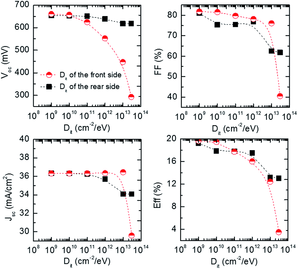
Fig. 3 shows the cells' performances as a function of the Dit at front and rear sides of the c-Si, respectively. Fig. 3a shows that Voc significantly decreases about 300 mV as the Dit at the front i-a-Si:H/p-c-Si interface increases from 109 cm−2 eV−1 to 1013 cm−2 eV−1 because of the increased interface recombination. While the Voc is not seriously affected as the increasing Dit of the rear side. However, it could be found that the fill factor (FF), short-circuit current density (Jsc), and conversion efficiency (Eff) have been seriously decreased when the Dit of the rear side increase to 1013 cm−2 eV−1.
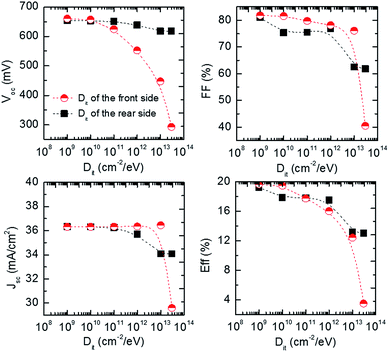 |
| | Fig. 3 The Voc, Jsc, FF and Eff of p-type solar cells as functions of the Dit at the front side and rear side of the solar cells. | |
The reason for this phenomenon could be ascribed to the relation between the Dit and the trapped charges at hetero-interface. As concluded from eqn (3) and (4), the Dit could directly impact on the Voc of the solar cells by changing band bending the recombination velocity of the front-side hetero-interface. Compared with the influences of front Dit on the device, the Dit of rear side has relatively small impact on the Voc. As most of the photons are absorbed at the front side of c-Si, the entire photo-generated carriers are separated (and transporting) basically rely on the built-in field established by front n-a-Si:H and p-type c-Si.24,25 Heterojunction established at the rear side is not the decisive factor for the Voc of the cells. The main function of the p+-a-Si:H BSF is to enhance carriers' selective holes-collection and transportation. Hence, the changed energy band structure of the rear p-c-Si/p+-a-Si:H junction has a relatively small impact on Voc compare with the one of n-a-Si:H/p-c-Si junction. However, the FF and Jsc are more sensitive to the rear-side Dit because of the band bending downward, which caused by high Dit (as shown in Fig. 2b), could induce the opposite electron current and creating a barrier for majority carrier (holes) transportation, thus increasing the series resistance of the p-type SHJ solar cells.
Analytical BSF's bandgap of p-type SHJ solar cells
The BSF layer should be included to obtain good cell performance. The offsets of the conduction band and valence band at heterojunction are:| | |
ΔEc = χc-Si − χa-Si:H
| (8) |
| | |
ΔEv = Ega-Si:H − χc-Si + χa-Si:H − Egc-Si
| (9) |
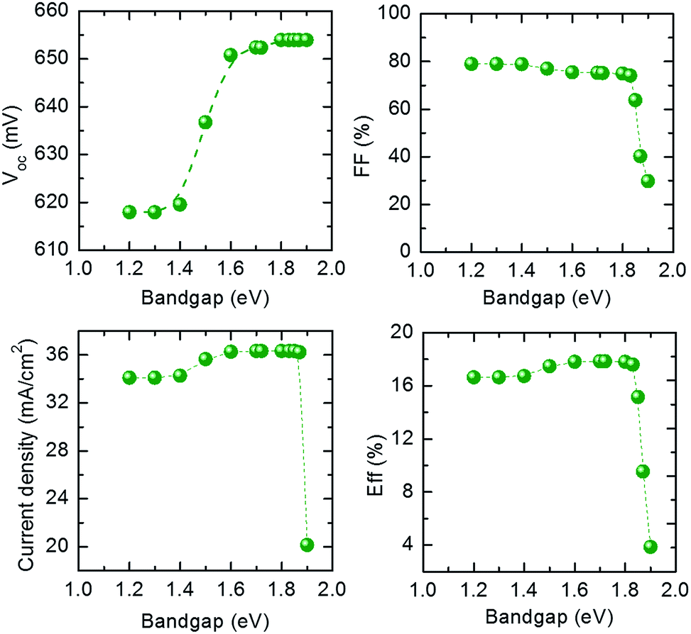
where χc-Si, χa-Si:H, Egc-Si and Ega-Si:H are the electron affinity and bandgap of c-Si and a-Si:H. The electron affinity of c-Si and a-Si:H is 4.05 eV and 3.9 eV, respectively. In practical experiment, the bandgap of the BSF could be adjusted by changing certain parameters of the p+-a-Si:H layer, such as the hydrogen content, doping concentration and crystallization.26,27 Fig. 4 shows the performance of the p-type SHJ solar cells as a function of BSF's bandgap. The Voc of the solar cells is improved significantly as the bandgap increased from 1.2 to 1.9 eV. The Jsc and FF of the solar cells are almost unaffected with the increasing of the bandgap of the BSF below 1.8 eV. While a pronounced decreasing could be found for Jsc and FF if further increasing the bandgap of the BSF to 1.9 eV.
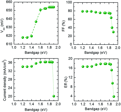 |
| | Fig. 4 The Voc, Jsc, FF and Eff of p-type solar cells as functions of the BSF's bandgap. | |
The band diagrams of the rear side p-c-Si/p+-a-Si:H structure are shown in Fig. 5, considering the BSF bandgap of 1.3 eV and 1.8 eV, respectively. The wide bandgap (1.8 eV) of BSF with a large conduction band offset could achieve good surface field for the rear-side diffusing electrons of the device.26–28 However, the valence band offset also increased, and hence establishing a large barrier for holes to flow through the rear contact. However, in contrast, the low bandgap of the BSF layer resulted in band bend downward and small conduction band offset. As illustrated for Fig. 2b, this is detrimental for electrons diffused forward and will increase the recombination possibility at rear surface.
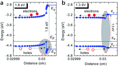 |
| | Fig. 5 Band diagrams of the rear-side heterojunction when the bandgap of the BSFs are (a) 1.8 eV and (b) 1.3 eV, respectively. | |
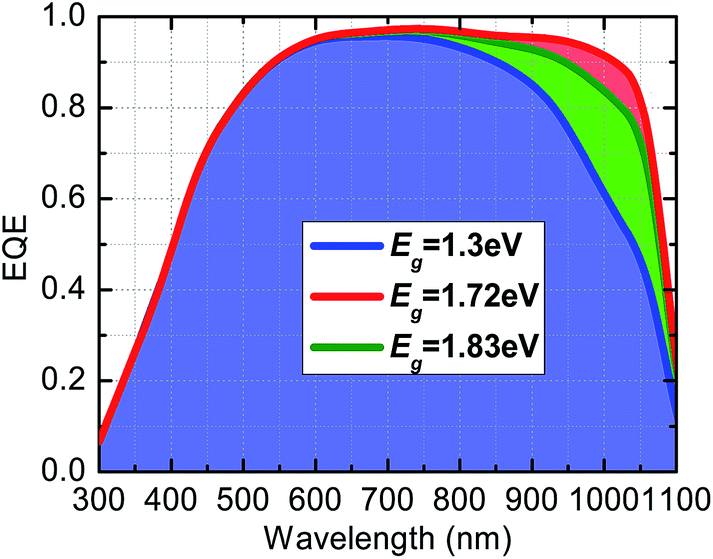
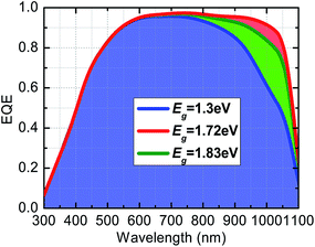
Fig. 6 shows the EQE variation with bandgap to further explain the previously described results. With the bandgap increased from 1.3 to 1.72 eV, the spectrum response at longer wavelengths increased due to the suppressing of the recombination, which caused by enhancing back surface field effect. However, further increasing the bandgap will decrease the spectrum response owing to the large valence band offset blocking the majority holes' transportation. Thus, it can be concluded that there exists a trade-off between surface field effect and carrier transportation barrier, and it could be relaxed by carefully regulating the bandgap of the BSF layer. Also, the numerical calculation results indicate that the optimum bandgap of BSF should be controlled in the range of 1.7 to 1.8 eV for p-type SHJ solar cells in practical processing.
 |
| | Fig. 6 The EQE curves of the p-type SHJ solar cells when the bandgap of the BSF layers variant from 1.3 eV to 1.8 eV. | |
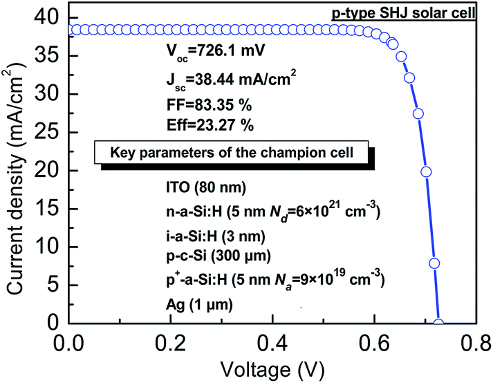
Finally, as shown in Fig. 7, when the defect states density at both side of the c-Si is 1010 cm−2 eV−1, and the bandgap of the BSF layer is 1.72 eV (the thickness of a-Si:H emitter layer and intrinsic layer is set as 5 nm and 3 nm respectively. The doping concentration of n-a-Si:H and p+-a-Si:H layers are 6 × 1021 cm−3 and 9 × 1019 cm−3 respectively), an efficiency of the 23.27% could be achieved. The performance of the solar cells as a function of the c-Si thickness has also been study, which has been shown in Fig. S1 and S2.† It should be noted that this results are obtained only based on planar p-type substrate without incorporating any antireflection coating and light trapping architecture. Hence, for p-type SHJ solar cells, a more than 24% efficiency could be expected with fully designed light-management strategies in practical application. Based on the performance and cost analysis, it is observed that besides n-type solar cells, the simple and low-cost p-type SHJ solar cells with optimized Dit and BSF layer may also be potential candidate for high efficiency solar cell technology.
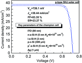 |
| | Fig. 7 Illuminated current density–voltage curve of the champion cell. All the optimized parameters are extracted from the practical experimental results. | |
4. Conclusions
In summary, the influence of interface defects at both side of c-Si and bandgap of BSF layer on p-type SHJ solar cell performance were investigated though numerical calculations. Hence, suggestive design parameters for p-type SHJ solar cell fabrication are proposed. The result shows that Dit at front and rear side of c-Si should be controlled lower than 1013 cm−3 to avoid significantly negative impact on the solar cells performance. Meanwhile, Dit at front side directly determine the values of Voc. While Dit at the rear side of the solar cell seriously affects the Jsc and FF. Appropriate designation for the bandgap of the BSF (1.7–1.8 eV) can improve the efficiency of the p-type SHJ solar cells by relaxing the trade-off between surface field effect and carrier transportation barrier. Finally, a conversion efficiency of more than 23% could be achieved by adopting the parameters extracted from experimental results. This highlights that SHJ solar cells based on low-cost p-type c-Si may also be the market-leading products owing to the improvements on cost-to-performance ratio for c-Si photovoltaics.
Acknowledgements
The authors gratefully acknowledge the support from National Nature Science Foundation of China (Grant No. 61475063, 61505067 and 21576111), Program for New Century Excellent Talents in University (No. NCET-13-0824).
References
- Y. Jia, J. Wei, K. Wang, A. Cao, Q. Shu, X. Gui, Y. Zhu, D. Zhuang, G. Zhang, B. Ma, L. Wang, W. Liu, Z. Wang, J. Luo and D. Wu, Adv. Mater., 2008, 20, 4594–4598 CrossRef CAS.
- Y. Jia, A. Cao, X. Bai, Z. Li, L. Zhang, N. Guo, J. Wei, K. Wang, H. Zhu, D. Wu and P. M. Ajayan, Nano Lett., 2011, 11, 1901–1905 CrossRef CAS PubMed.
- M. Lu, S. Bowden, U. Das and R. Birkmire, Appl. Phys. Lett., 2007, 91, 063507 CrossRef.
- Y. Liu, J. Zhang, H. Wu, W. Cui, R. Wang, K. Ding, S.-T. Lee and B. Sun, Nano Energy, 2017, 34, 257–263 CrossRef CAS.
- F. Wang, R. Du, Q. Ren, C. Wei, Y. Zhao and X. Zhang, J. Mater. Chem. C, 2017, 5, 1751–1757 RSC.
- K. Yoshikawa, H. Kawasaki, W. Yoshida, T. Irie, K. Konishi, K. Nakano, T. Uto, D. Adachi, M. Kanematsu, H. Uzu and K. Yamamoto, Nat. Energy, 2017, 2, 17032 CrossRef.
- D. Macdonald and A. Cuevas, Phys. Rev. B: Condens. Matter Mater. Phys., 2003, 67, 075203 CrossRef.
- N. Jensen, U. Rau, R. M. Hausner, S. Uppal, L. Oberbeck, R. B. Bergmann and J. H. Werner, J. Appl. Phys., 2000, 87, 2639–2645 CrossRef CAS.
- G. D. Cody, T. Tiedje, B. Abeles, B. Brooks and Y. Goldstein, Phys. Rev. Lett., 1981, 47, 1480–1483 CrossRef CAS.
- A. A. Langford, M. L. Fleet, B. P. Nelson, W. A. Lanford and N. Maley, Phys. Rev. B: Condens. Matter Mater. Phys., 1992, 45, 13367–13377 CrossRef CAS.
- P. Biswas, D. Paudel, R. Atta-Fynn, D. A. Drabold and S. R. Elliott, Phys. Rev. Appl., 2017, 7, 024013 CrossRef.
- M. Garín, U. Rau, W. Brendle, I. Martín and R. Alcubilla, J. Appl. Phys., 2005, 98, 093711 CrossRef.
- Z. Shu, U. Das, J. Allen, R. Birkmire and S. Hegedus, Progress in Photovoltaics: Research and Applications, 2015, 23, 78–93 CrossRef CAS.
- M. Schmidt, L. Korte, A. Laades, R. Stangl, C. Schubert, H. Angermann, E. Conrad and K. V. Maydell, Thin Solid Films, 2007, 515, 7475–7480 CrossRef CAS.
- S. Avasthi, S. Lee, Y.-L. Loo and J. C. Sturm, Adv. Mater., 2011, 23, 5762–5766 CrossRef CAS PubMed.
- M. Smeets, K. Bittkau, F. Lentz, A. Richter, K. Ding, R. Carius, U. Rau and U. W. Paetzold, Nanoscale, 2016, 8, 18726–18733 RSC.
- M. Agarwal, A. Pawar, N. Wadibhasme and R. Dusane, Sol. Energy, 2017, 144, 417–423 CrossRef CAS.
- J. Yu, J. Bian, W. Duan, Y. Liu, J. Shi, F. Meng and Z. Liu, Sol. Energy Mater. Sol. Cells, 2016, 144, 359–363 CrossRef CAS.
- S. Olibet, E. Vallat-Sauvain, L. Fesquet, C. Monachon, A. Hessler-Wyser, J. Damon-Lacoste, S. De Wolf and C. Ballif, Phys. Status Solidi A, 2010, 207, 651–656 CrossRef CAS.
- M. Mikolášek, J. Racko and L. Harmatha, Appl. Surf. Sci., 2017, 395, 166–171 CrossRef.
- R. Hussein, D. Borchert, G. Grabosch and W. R. Fahrner, Sol. Energy Mater. Sol. Cells, 2001, 69, 123–129 CrossRef CAS.
- S.-C. Shiu, J.-J. Chao, S.-C. Hung, C.-L. Yeh and C.-F. Lin, Chem. Mater., 2010, 22, 3108–3113 CrossRef CAS.
- Y. Zhang, C. Yu, M. Yang, Y. He, L. Zhang, J. Zhang, X. Xu, Y. Zhang, X. Song and H. Yan, RSC Adv., 2017, 7, 9258–9263 RSC.
- L. Mazzarella, S. Kolb, S. Kirner, S. Calnan, L. Korte, B. Stannowski, B. Rech and R. Schlatmann, in 2016 IEEE 43rd Photovoltaic Specialists Conference (PVSC), 2016, pp. 2955–2959 Search PubMed.
- K. Ding, X. Zhang, F. Xia, R. Wang, Y. Kuang, S. Duhm, J. Jie and X. Zhang, J. Mater. Chem. A, 2017, 5, 285–291 CAS.
- M. H. Brodsky, M. Cardona and J. J. Cuomo, Phys. Rev. B: Condens. Matter Mater. Phys., 1977, 16, 3556–3571 CrossRef CAS.
- J. Kakalios, R. A. Street and W. B. Jackson, Phys. Rev. Lett., 1987, 59, 1037–1040 CrossRef CAS PubMed.
- L. Zhao, G. Wang, H. Diao and W. Wang, Phys. Status Solidi RRL, 2016, 10, 730–734 CrossRef CAS.
Footnote |
| † Electronic supplementary information (ESI) available. See DOI: 10.1039/c7ra04018k |
|
| This journal is © The Royal Society of Chemistry 2017 |
Click here to see how this site uses Cookies. View our privacy policy here. 
 Open Access Article
 This Open Access Article is licensed under a
  a,
Yanbo Gaoa,
Zhenyu Pangabc,
Lili Yang*a and
Jinghai Yang*a
a,
Yanbo Gaoa,
Zhenyu Pangabc,
Lili Yang*a and
Jinghai Yang*a