
 Open Access Article
 This Open Access Article is licensed under a
 Creative Commons Attribution 3.0 Unported Licence
Graphene based nanosensor for aqueous phase detection of nitroaromatics
S. Avaz *a,
R. B. Roya,
V. R. S. S. Mokkapati*b,
A. Bozkurta,
Santosh Panditb,
Ivan Mijakovicb and
Y. Z. Mencelogluacd
*a,
R. B. Roya,
V. R. S. S. Mokkapati*b,
A. Bozkurta,
Santosh Panditb,
Ivan Mijakovicb and
Y. Z. Mencelogluacd
aSabanci University, Faculty of Engineering and Natural Sciences, 34956 Tuzla, Istanbul, Turkey. E-mail: senemavaz@sabanciuniv.edu
bChalmers University of Technology, Department of Biology and Biological Engineering, Division of Systems and Synthetic Biology, Goteborg, Sweden. E-mail: ragmok@chalmers.se
cSabanci University Integrated Manufacturing Technologies Research and Application Center & Composite Technologies Center of Excellence, Teknopark, 34906 Pendik, Istanbul, Turkey
dSabanci University Nanotechnology Research and Application Center, 34956, Istanbul, Turkey
First published on 12th May 2017
Abstract
A graphene-based nanosensor was fabricated to selectively detect nitrotriazolone (NTO) molecules with a molecularly imprinted film via simple electrical measurements. Molecularly imprinted polymer comprising chitosan was used as sensitive layer. Gold electrodes for electrical measurements were lithographically fabricated on Si/SiO2 substrate, followed by monolayer graphene transfer and polymeric film coating. Monolayer graphene and molecularly imprinted polymer were characterized by ATR-FTIR, UV-Vis, SEM and Raman spectroscopy. Transfer-length measurements (TLM) indicate that the sensor selectively and linearly responds against aqueous NTO solutions within a wide range of concentration of 0.01–0.1 mg mL−1 that covers the lowest toxic level of NTO determined by USEPA. This nanosensor with embedded electrodes is re-usable and suitable for field applications, offering real-time electrical measurements unlike current techniques where complex analytics are required.
Introduction
Chemical sensors have found considerable applications in the fast detection of explosives for mining, environmental, forensic and criminal research and in the improvement of explosive production.1,2 There are several approaches for the detection of nitroaromatic compounds, from low precision indirect determination of metal covered explosives to high sensitive spectroscopic determination of trace amounts. Low precision methods are useful to detect traditional landmines and arms, but are inadequate in further applications such as airport scanning and flight safety. On the other hand, high sensitive methods require sophisticated instrumentation including gas chromatography-mass spectroscopy,3 Raman spectroscopy,4 energy dispersive X-ray diffraction5 and cyclic voltammetry,6 therefore are incompatible with field applications. With its sensitivity in pico-to nanogram levels, ion mobility spectroscopy is a frequently used technique in airport safety with high cost, requiring frequent calibration and may give false positives liable to operator.7Considering the ecological effects along with determination and location nitroaromatics,8,9 analyte interferences during sampling from water and soil poses a problem for detection systems. As a result, determination of trace amounts of chemicals in soil samples is limited to their volatile components and/or side products of the material.10 Polymeric absorbers are employed to help increase the signal strength since the vapour pressures of explosives are relatively low. In these systems, volatile component is condensed on detection system and physically/chemically adsorbed on the polymeric material's pores. Therefore, vapour pressure of volatile component is the dominant factor in determining response time of the sensor, while detection limit requires volatile amounts of the component that is enough to be detected by the system. According to United States Environmental Protection agency (USEPA) criteria for environmental health and safety,11 it is important to consider the difficult sampling conditions, and necessity of bulk amounts of analyte required for detection, it is of utmost importance to develop high-sensitivity methods to detect trace amount of nitroaromatics. Although the toxicity tests resulted in low toxicity values for nitroaromatic compound of nitrotriazolone (NTO), the lowest observed adverse effect level values of 2,4,6-trinitrotoluene (TNT) and NTO are 0.5 mg kg−1 day−1 and 30 mg kg−1 day−1, respectively.12 Along with USEPA criteria for explosives,13 taking environmental factors into consideration, highly sensitive methods are required to detect these type of chemicals.
Nano-scale systems provide numerous alternatives to develop detection systems with the limits mentioned above. Here, the prefix “nano-” defines systems with high sensitivities that are able to detect below the limits of macro-sized materials. Therefore, nanosensors enhance the observability of chemical and physical properties. In addition, highly evolved fabrication, sensing and detection techniques improve the in-signal transforming performance.14 There are various nano-sized detection elements/platforms available in the literature including quantum dots,15 nano-wires,16 and nanotubes.17 Utilization of graphene in nanosensor systems in nitroaromatics detection was first reported in 2010.18 As a 2D carbon material, graphene has superior electrical properties19 arising from effective π–π interactions and homogenous distribution of electrochemically active sites.20,21 In addition to this, extraordinary electronic band structure enables graphene to behave as a zero-bandgap semi-conductor22 and the considerable surface area allows adsorbent materials to significantly change its electrical properties by altering carrier density. The high sensitivity of graphene also arises from low electrical signal noise due to its 2D crystal network structure.23 All those findings indicate graphene to be available to respond electrically, even in very low concentrations of analyte and therefore suitable for nanosensor applications.
Detection of nitroaromatics using graphene was first carried out by coating graphene on a glassy electrode,24 and was followed by many others.20,25 Majority of the studies employing graphene as a transistor were based on electrochemical measurements. Although fabrication and measurement techniques are relatively simple, selectivity is rather limited in electrochemical systems.14
Several polymeric systems were employed for the detection of nitroaromatics using physical, structural and electronic interactions between analyte and polymeric material.26,27 Primary concern in developing new sensors is to collect adequate amount of recognition/binding element in the sensor probe. In this aspect, molecularly imprinted polymers possess various advantages such as varying selectivity and low cost. General approach in sensor design is to utilize sensor probes with high specificity against analyte. Yet, in ecological samples, analyte is notably in very low concentrations and mostly surrounded by a matrix composing similar molecules. Therefore, even systems employing high selectivity enzymes as sensor probes are prone to cross-reactivity and false positives.28 As a solution to this, molecularly imprinted polymers offer specific and selective cavities of analyte within the polymer surface stabilized by inter-molecular crosslinking, thus ensuring physical and/or chemical interactions with the analyte.29–31 In addition, molecularly imprinted polymers are also superior to traditional polymers in terms of high thermal, chemical and mechanical stability,32 therefore it is considerably reasonable to employ molecularly imprinted polymers as sensor probes. As a natural poly amino saccharide with available amino and hydroxyl functional groups, chitosan is a feasible polymer for crosslinking, hence molecular imprinting. In addition, crosslinked chitosan acts as a supporting matrix due to its superior film forming ability33 and increased mechanical properties arising from crosslinking.34 Vast amounts of available amino and hydroxyl groups also provide strong secondary interactions with nitroaromatics and thus ensure adsorption. These above mentioned properties of chitosan make it a promising candidate for nanosensor applications for explosives35 with no further need of additional film component.
An approach to increase the selectivity in nanosensors is to use hybrid systems, thus obtaining orthogonal or enhanced signal by gathering different sensing mechanisms.34 Hybrid systems comprising graphene are usually composed of a graphene layer and a polymer. Recently, several examples of such systems used for explosive detection are found in the literature36–38 but mostly centred around TNT and use sophisticated instrumentation for signal transduction.
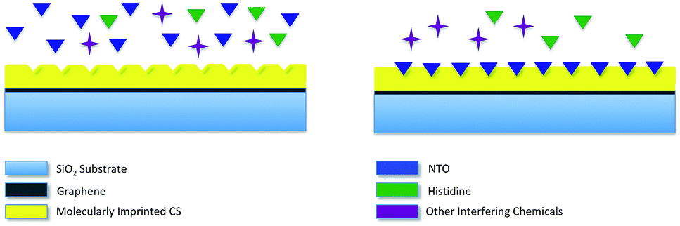
Molecular imprinting creates binding sites in polymeric film surface that is specific to template molecules. In a standard molecular imprinting process, template molecules are introduced to polymer during crosslinking. In the meantime, crosslinked polymer assembles around template molecule to create specific binding sites. These binding sites interact with the analyte both through lock–key mechanism and via secondary interactions. This way, highly selective polymeric films/matrices are obtained. When exposed to the analyte, polymeric film reversibly adsorbs analyte molecules. This adsorption results in increasing the charge of the polymeric film, thus altering the resistance of bottom layer (graphene). The sensing mechanism via molecular imprinting is explained in Fig. 1.
 | ||
| Fig. 1 Schematic representation of molecular imprinting and recognition mechanism employed in nanosensor. | ||
The purpose of this study is to develop a hybrid nanosensor to detect NTO by adsorbing nitroaromatic compound on molecularly imprinted chitosan film and to determine the amount of adsorbed species via the change in resistivity of monolayer graphene sheet. To do this, monolayer graphene was transferred onto SiO2 substrate, and coated with molecularly imprinted polymer film. Metallic electrodes were embedded into substrate by lithography prior to graphene transfer. Here, NTO was chosen as the target molecule since it is a new generation insensitive explosive, thus a possible replacement for TNT. Selectivity and sensitivity of the fabricated nanosensor was tested against analyte and a chemical compound that is similar to NTO in molecular structure (Histidine). Real sample measurements were also carried out to test the effect of other possible interfering chemicals present in water and soil samples. Although it has been widely used in nitroaromatics detection as film substrate, molecularly imprinted chitosan was used as a direct sensor probe for the first time without needing any further component to increase the signal strength or to ensure interaction. In addition, a unique micro fabrication technique was applied where the electrodes to measure the change in sheet resistance of graphene due to molecularly imprinted polymer-analyte attractions were embedded in sensor substrate. To our knowledge this is the first time where such a technique has been used, unlike other methods where electrodes were usually fabricated on graphene for transfer length measurements (TLM). By this process, contamination of graphene or other interfering species during fabrication and measurements were eliminated.
Experimental
Preparation of molecularly imprinted chitosan films
Molecular imprinting was carried out to ensure non-covalent interactions between polymeric film and NTO molecules. For this purpose, acetic acid solution (1%) of chitosan (CS) and NTO was introduced with glutaraldehyde (GA) and stirred for 5 minutes. The mixture was then spin-coated onto a CVD graphene substrate. As a negative control, non-imprinted films were prepared in the absence of NTO. Amount of NTO and glutaraldehyde added were explained in Table 1. Resulting films were characterized by ATR-FTIR spectroscopy. Swelling kinetics of the films was studied in detail along with its effect on NTO adsorption capacity.| Code | NTO/CS ratio (m m−1) | CS/GA ratio (m V−1) |
|---|---|---|
| CSNIP1 | — | 0.02 |
| CSNIP2 | — | 0.04 |
| CSNIP3 | — | 0.08 |
| CSNIP4 | — | 0.16 |
| CSNTO-N1 | 0.2 | 0.02 |
| CSNTO-N2 | 0.4 | 0.02 |
| CSNTO-N3 | 0.6 | 0.02 |
| CSNTO-N4 | 0.8 | 0.02 |
| CSNTO1 | 0.4 | 0.02 |
| CSNTO2 | 0.4 | 0.04 |
| CSNTO3 | 0.4 | 0.08 |
| CSNTO4 | 0.4 | 0.16 |
ATR FTIR spectroscopy
ATR-FTIR spectra of crosslinked films were collected on a Bruker Equinox 55 ATR-FTIR spectrometer from 550 to 4000 cm−1, with a resolution of 0.5 cm−1. A total of 32 scans were gathered and baseline-corrected.UV-Visible spectroscopy
Capacities of NTO adsorption of molecularly imprinted films were measured in terms of the decrease in visible light absorption of NTO solutions exposed to molecularly imprinted chitosan films, compared to that of non-imprinted films. Spectra were collected using Schimadzu UV3600 Plus Ultraviolet, visible and near-IR spectrometer. Selectivity studies, along with desorption kinetics were carried out using UV-Visible spectroscopy.Fabrication of metallic contact lines
Since graphene monolayers are sensitive to minute mechanical strain, it is absolutely necessary to make the substrate surface as flat as possible after patterning the metallic contact lines. A simple micro-fabrication process where metallic structures can be embedded inside a substrate is adapted for the currently used thermally oxidized silicon substrate (1 micron oxide layer). A mask (Fig. 2(e)) with TLM contact line patterns was aligned on the sample wafer and was etched with silicon hexafluoride based DRIE recipe, depicted in Table 2. | ||
| Fig. 2 Schematic representation of fabrication steps and details of fabricated nanosensor; Si/SiO2 substrate (a); etched and Cr/Au deposited substrate (b); monolayer graphene transfer and molecularly imprinted polymer spin-coating (c); layer-wise sensor view (d); top-view with TLM pattern length details (e), side-view (f), and details of side view (g); fabricated nanosensor (h). All dimensions in (e) are in mm. | ||
| SF6 flow rate | 45 sccm |
|---|---|
| Pressure | 7.5 × 10⁻⁹ Torr |
| DC forward power | 50 Watts |
| ICP forward power | 2000 Watts |
| Table temperature | 10 °C |
| Silicon di oxide etch rate | ∼2.2 nm s−1 |
In the next step, e-beam evaporator (NanoVak NVTE4-01 Thermal Evaporator) was used to deposit a Cr adhesion layer of 20 nm thicknesses, followed by the deposition of a 100 nm thick thermally evaporated Au electrode, without removing the mask. This resulted in a perfectly flat substrate with embedded metallic TLM lines. In order to see the effect of employing photolithography on flatness, soft mask prepared for photolithography was replaced with a hard mask. Fig. 2(a–d) depicts the fabrication steps, while Fig. 2(e–g) shows the top and cross-sectional views of the sample after the deposition of graphene and polymer films. An actual image of the nanosensor is presented in Fig. 2(h).
Monolayer graphene transfer onto Si/SiO2 substrate
Graphene transfer was carried out as described in the literature.39,40 Monolayer graphene on Copper foil (Graphene Supermarket, USA) was first spin-coated with poly methyl methacrylate (950 PMMA C2 Resist; Micro Chemicals GmbH) and heat-treated to prevent breakage during transfer. Backside of graphene was etched using Oxygen Plasma Asher to remove additional carbon species that might stick to graphene sample in further steps. Copper foil was then etched in aqueous ammonium persulfate solution (10%) and resulting monolayer graphene + PMMA was transferred on to a Si/SiO2 substrate followed by PMMA removal in acetone. Monolayer graphene was characterized by Raman Spectroscopy.Scanning electron microscopy
The surface of the substrate with metallic contact lines and graphene was investigated by scanning electron microscopy. For this purpose, samples were sputter coated with a thin layer of Pt/Pd. Images were acquired by SEI detector, using an electron gun voltage of 2 kV.Raman spectroscopy
Raman spectra of graphene samples transferred onto glass substrate were obtained at 532 nm visible excitation using Renishaw InVia Reflex Raman Spectrometer attached to a microscope.Electrical measurements
The change in resistance of monolayer graphene due to NTO adsorption onto molecularly imprinted chitosan was measured by two-probe setup (Cascade MicroTech PM5 Probe Station). Sheet resistance of graphene was calculated by linear fit of eqn (1).| RTotal = (Rsheet/Wchannel)d + 2Rcontact | (1) |
Eqn (1) total resistance as a function of sheet resistance of graphene and contact resistance.
Results and discussion
Chemical characterization of molecularly imprinted films
Fig. 3(a) shows the attenuated total reflectance (ATR)-FTIR spectrum of native CS. The band at 1149.94 cm−1 and overlapped bands round 1022 cm−1 are attributed to asymmetric C–O vibrations resulting from deacetylation and C–OH and C–O–C vibrations of the β-(1-4)-linked D-glucosamine (deacetylated unit) and N-acetyl-D-glucosamine (acetylated unit) rings, respectively. In addition, the absorption bands at 1314.56 cm−1 are attributed to C–H bending of –CH2 groups, while the one at 1373.56 corresponds to C–O stretching mode of –CH2–OH groups. The peaks within the range of 1589.79–1651.34 cm−1 correspond to the bending mode of primary amino groups and carbonyl stretching, respectively. The broad absorbance band in the region of 2862.72 cm−1 corresponds to symmetric and asymmetric stretching of the aliphatic –CH2 and –CH3 groups. The wide peak centred at 3287.05 cm−1 originated from –OH groups along with H-bonding. | ||
| Fig. 3 FTIR spectra of native (a), crosslinked, non-imprinted (b) and NTO imprinted chitosan (c). | ||
Crosslinked CS samples showed similar FTIR bands to CS, with slight shifts, within the range of 800–1200 cm−1 that corresponds to main saccharide ring. Different than native CS, crosslinked non-imprinted (b) and NTO-imprinted (c) CS spectra showed some additional vibrations. For instance, the newly formed bands around 1550 cm−1 in crosslinked species revealed the existence of quaternary amino groups.41 Moreover, the sharp band around 1636 cm−1 of C![[double bond, length as m-dash]](https://www.rsc.org/images/entities/char_e001.gif) N vibrations proved the formation of Schiff's base upon crosslinking.
N vibrations proved the formation of Schiff's base upon crosslinking.
pH & swelling kinetics
Swelling kinetics was investigated by subjecting imprinted and non-imprinted CS gels with different GA amounts to 2% acetic acid solutions. Swelling degree was calculated from the weight ratio between dry and swelled gels. Fig. 4(a) suggested that a non-usual swelling trend was observed in CSNIP gels due to the presence of free amino-functional groups. On the other hand, an inverse proportion between crosslinker amount and swelling was observed in CSNTO gels implying that the network gets more rigid with increased crosslinker amount. Considering high crosslinking with a low swelling degree of CSNTO films as the selection criteria, the optimum range of crosslinker amount was determined as 8–12%. Furthermore, it was also observed that films prepared with 12% crosslinker were brittle and easily broken during measurements. Therefore, 8% was chosen as optimum crosslinker concentration.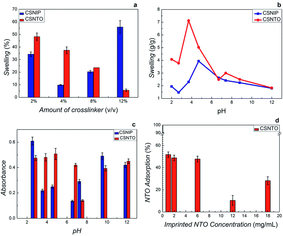 | ||
| Fig. 4 Effect of pH on swelling (a) and on NTO adsorption (b) with respect to crosslinker amount; effect of crosslinker amount on swelling (c); and amount of imprinted NTO on NTO adsorption of molecularly imprinted films (d). Non-imprinted films are shown in blue and imprinted films are shown in red. | ||
Once the crosslinker amount was optimized, the effect of pH on swelling (Fig. 4(b)) and NTO adsorption capacities of films (Fig. 4(c)) were tested by exposing gels to 0.1 mg mL−1 NTO solutions prepared in different pH buffers. Immersed films were then compared to original solutions in terms of UV-Vis absorption. As seen in Fig. 4(b), lowest degree of swelling was observed at pH 6.7 and 12.0 for both gels. Although NTO adsorption capacity of CSNTO was significantly higher between pH 3.7–4.7, a very significant swelling, up to 7× was observed in NTO imprinted CS around these pH values (Fig. 4(c)). Therefore, this region was omitted. In addition, Fig. 4(c) also suggested that NTO adsorption of CSNTO was significantly higher than that of CSNIP at pH 6.7. Considering lower swelling and higher NTO adsorption, an optimum pH value of 6.7 was selected and further measurements were carried out at this pH value.
Effect of NTO amount on molecular imprinting
Effect of NTO amount on imprinting was investigated by UV-Vis spectroscopy. For this purpose, chitosan–NTO solutions were prepared in different NTO amounts (Table 3). Chitosans were crosslinked by glutaraldehyde (1%) and left to gelate. After washing, gels were exposed to NTO solutions (1 mg mL−1) and UV-Vis spectra were recorded and compared to reference NTO solution.| Sample Name | Imprinted NTO amount (g) | Amount CS (mL) |
|---|---|---|
| CSNTON1 | 0.05 | 50 |
| CSNTON2 | 0.1 | 50 |
| CSNTON3 | 0.3 | 50 |
| CSNTON4 | 0.6 | 50 |
| CSNTON5 | 0.9 | 50 |
UV-Vis spectroscopy revealed that NTO adsorption was minimum around 12–18 mg mL−1 NTO concentrations (Fig. 4(d)), while it enhances significantly with the reduction in NTO in gel preparation medium. In addition, it was observed that high concentrations of NTO increase the crosslinking time (crosslinking resulted in viscous liquids rather than a rigid gel). We presume that high amounts of NTO aggregate and block the crosslinking regions of polymer chains. Taking these parameters into consideration, optimum amount of NTO in imprinting was determined as 1–2%.
Micro fabrication
Fig. 5 shows microscopic images of levelled (flat) (a) and unlevelled (b) gold electrodes before graphene transfer; SEM images of unlevelled (c) and levelled (d) after graphene transfer.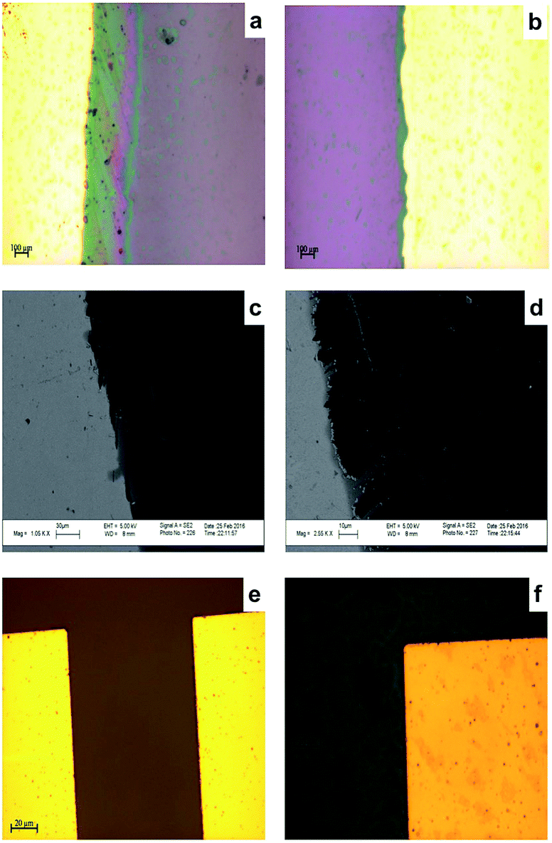 | ||
| Fig. 5 Optical microscopic images of graphene on unlevelled (a) and levelled (b) gold electrodes; SEM images of graphene on unlevelled (c) and levelled (d) gold electrodes. Optical microscopy images of levelled gold electrodes (yellow) on SiO2 substrate (brown) fabricated by photolithography without (e) and with (f) graphene. | ||
It was observed from optical microscopy and SEM images that after graphene transfer (Fig. 5(a and b)) levelling by photolithography, instead of using hard mask is a crucial step in micro fabrication. SEM images of graphene on an unlevelled gold–Si/SiO2 (Fig. 5(c and d)) substrate revealed that graphene was scratched when transferred on unlevelled substrate. Therefore, height profiles should be carefully investigated following each gold deposition. On the other hand, Fig. 5(e–f) demonstrates optical microscopic images of sensor following photolithography. Comparing the optical microscopic images of sensors fabricated with a hard mask (a) and a soft mask (b) with same TLM patterns, it was observed that the edge groove and unevenness is considerably cured when a soft mask was employed.
Monolayer graphene characterization
Raman spectroscopy was employed to confirm monolayer graphene. For graphene samples, two characteristic Raman peaks were observed due to a stokes phonon energy arising from laser excitation. The first one, G band observed at 1593 cm−1, corresponds to primary in-plane vibrations, whereas the second one, 2D band observed at 2689 cm−1, accounts for a second order two-phonon process exhibited by all sp2 carbon materials. 2D is the highest intensity peak in a single layer graphene spectrum and along with G band; it can be used to determine the number of layers of a graphene sample. In multi-layer graphene 2D peak is split into four and reduces in intensity. As seen in Fig. 6, our sample showed 2D > G behaviour in band intensity from different regions, therefore monolayer graphene was confirmed. | ||
| Fig. 6 Raman spectrum of monolayer graphene (a), and microscopy image of the area Raman data was gathered (b). | ||
TLM measurements and sensitivity studies
Prior to polymer coating, sheet resistance of graphene on SiO2 was measured by TLM and determined as 418,2 ohm sq−1 which correlated well with the literature data.42 With 160 nm polymer coating, this value was increased to 694,1 ohm sq−1 due to the introduction of low-conducting layer (0.25 ± 0.09 S m−1)43 when compared to monolayer graphene (2.62 × 10² S m−1).44A series of TLM measurements were carried out to determine the sensitivity of fabricated nanosensor by exposing sensors to NTO solutions in different concentrations. Subjecting to increasing current, I–V measurements were carried out and sheet resistances were calculated by the slope of resistance curves at increased contact pair distances. Sensor fabricated using NTO imprinted CS was treated with NTO solutions and TLM measurements were carried out following air-drying. TLM measurements were carried out in concentration and current range of 0.01–0.1 mg mL−1 and 0.01–0.1 mA, respectively. This way, a standard curve was obtained for each NTO concentration value. Sheet resistances were obtained from slopes of standard curves and plotted against corresponding NTO concentration. Results show that sensor fabricated using NTO imprinted CS gave linear response to increased NTO concentration in the range of 0.01–0.1 mg mL−1. Therefore, measurement limits were determined as 0.01 and 0.1 mg mL−1. This detection limit is acceptable considering that the sensor probe is composed of a polymeric thin film. Table 4 summarizes high performance nitroaromatic sensors found in the literature, their type of measurement, detection limits and response times. Comparing literature examples to our sensor,45–57 one can conclude that there are sensor studies available in the literature with better response times and low detection limits, nevertheless most of these methods rely on vapour-phase detection of nitroaromatics. This type of detection can be challenging due to the low vapor pressure of these nitroaromatics. In addition, most of the measurements require sophisticated instrumentation. In our case, fabricated nanosensor is advantageous in terms of ease of measurement (a simple I–V test) with wide linear range.
| Sensor type | Measurement type | Detection limit | Response time (min) | Ref. |
|---|---|---|---|---|
| a VP: vapour phase. | ||||
| Molecularly imprinted polymer thin film-graphene | Electrical | 10–100 ppm | <5 | This work |
| Electrochemical gas sensor | Electrochemical-VPa | 50–500 ppm | 10–20 | 45 |
| Siloxane | Surface acoustic wave (SAW)-VP | 235 ppt | 0.84 | 46 |
| Carbowax-silica | SAW-VP | 300 ppb | 1 | 47 |
| Molecularly imprinted cyclodextrin | SAW-VP | 600 ppb | 5 | 48 |
| Dye embedded copolymer | Colorimetric | 0.2 ng | — | 49 |
| Polyacetylene thin film | Fluorescence quenching-VP | ppb level | <20 | 50 |
| SiO2-modified electrode | Cathodic voltammetry | 1.8 nM | — | 51 |
| Fluorescent paper | UV | 0.5 ppm | 0.5 | 52 |
| Perovskite-reduced graphene oxide | GCE-cyclic voltammetry | 0.3–0.8 μM | — | 53 |
| PVA membrane | Fluorescence-optical | 5.0 × 10⁻⁶ M | 1 | 54 |
| Graphene film | GCE-differential pulse voltammetry | 1–200 ppb | 1 | 55 |
| Reduced graphene oxide | GCE-stripping voltammetry | 5.49 × 10⁻⁷ M | — | 56 |
| Polystyrene-gelatin double layer | Fluorescence quenching-VP | — | 20 | 57 |
Selectivity studies
Selectivity studies were carried out by comparing the TLM results obtained from NTO-imprinted and non-imprinted sensors. It was found out that non-imprinted sensor was insensitive to any change in NTO concentration. It was also observed that sheet resistance values obtained from non-imprinted polymer were relatively higher compared to the imprinted ones. This may be due to the fact that non-imprinted polymer non-selectively adsorbs different species present in the solution. Comparisons of sheet resistance results obtained from NTO-imprinted and non-imprinted sensor are shown in Fig. 7. | ||
| Fig. 7 Selectivity comparison of non-imprinted (CSNIP) sensor to -imprinted (CSNTO) against NTO and histidine (blue scale is also valid for histidine values). | ||
Selectivity studies also include the response of molecularly imprinted sensor to another chemical compound that is similar to NTO in molecular shape. To evaluate this, CSNIP and CSNTO sensors were exposed to 0.1 mg mL−1 histidine solutions and TLM sheet resistance values were re-calculated. It was observed that CSNTO sensor resulted in significantly higher sheet resistance values when treated with histidine, whereas non-imprinted sensor gave a sheet resistance value that was in the same order with the ones exposed to NTO. In other words, CSNIP failed to distinguish analyte from other chemicals, and did not to respond selectively against different concentrations of NTO. On the other hand, CSNTO sensor is selective against NTO analyte, and does not respond to other species, even when a structurally similar chemical is introduced. Sheet resistance values obtained from NTO and histidine treatment of same concentrations are also shown in Fig. 7.
Interference test
NTO solution and histidine–NTO mixture was prepared in tap water to see the interference effect of chemicals with similar structure and commonly interfering charged particles (Cl2+, Mg2+, Na+). CSNTO sensor was treated with solutions containing 0.1 mg mL−1 NTO and above-mentioned chemicals. TLM measurements revealed that sensor response is similar to pure NTO solution. Therefore, we conclude that histidine and other interfering chemicals did not have any significant effect on TLM measurements and the detection method is able to distinguish analyte from bulk. Interference test also showed that the sensor can be used for real sample measurements and is suitable for field applications. Results of interference measurement are demonstrated in Table 5.| Blank | NTO (in pure water) | NTO (in bulk) | NTO + histidine (in bulk) | |
|---|---|---|---|---|
| Resistance (ohm sq−1) | 836.0 | 574.2 | 555.8 | 540.0 |
Response time & noise
Noise and response time measurements were carried out by immersing CSNTO sensor into 0.1 mg mL−1 NTO solution. Sheet resistance was recorded with respect to time. Results revealed that the response time of CSNTO sensor is less than 5 minutes (Fig. 8(a)). In addition, it was observed that the data converged to a sheet resistance value of 574,2 ohm sq−1, which correlated well with previous sheet resistance value for 0.1 mg mL−1 NTO (shown in Fig. 7). This also implies that CSNTO sensor read reproducible sheet resistance values for same concentrations of analyte. In addition, noise level of the sensor determined as ±0.5 mV (Fig. 8(b)). | ||
| Fig. 8 Response time measurements of CSNTO sensor for 0.1 mg mL−1 NTO solution (a) and noise measurement during a (b). | ||
Conclusions
We have successfully fabricated molecularly imprinted chitosan-graphene nanosensor and linearly detected explosive NTO molecules in the range of 0.01–01 mg mL−1 analyte concentrations.Fabrication started with embedding electrodes into a non-conducting substrate, which is, to our knowledge, a unique technique in TLM pattern formation, followed by graphene transfer and polymeric film coating. It was noted that levelling of metallic electrodes with substrate, in other words, creating a flat surface after electrode embedding is a crucial step in sensor fabrication, since graphene was prone to breakage when transferred on unlevelled substrates. Following graphene transfer, monolayer graphene was verified by Raman spectroscopy and it was observed that graphene was successfully transferred and was continuous without any breakage. The performance of molecularly imprinted polymeric film was investigated and the amounts of NTO and crosslinker required for imprinting were determined along with optimum pH range and swelling. TLM measurements were carried out successfully, and was observed that imprinted film responded linearly to increased NTO concentration in the targeted range, which covers the lowest observed adverse effect level value of NTO determined by USEPA. Therefore, toxic levels of NTO are within the detectible limits of the developed sensor. In addition, employing molecularly imprinted polymeric films as sensor probe is advantageous in detecting analytes in a linear fashion since non-imprinted polymer failed to give a linear response region. Moreover, a chemical compound with a similar molecular shape was tested with the fabricated sensor in order to verify the lock-key model between molecularly imprinted film and analyte. Interference test also confirmed that sensor is successful in distinguishing analyte in the presence of molecules with similar shape, and common interfering chemicals. It was concluded that sensor with molecularly imprinted polymeric film was insensitive against this compound, whereas sensor with non-imprinted produced false positives with chemical compounds in similar shapes. In other words, molecular imprinting was not only important in terms of giving a linear response region for analyte, but it also served to increase the selectivity of polymeric film in the range of linear response.
To sum up, a molecularly imprinted polymer-graphene based nanosensor was developed to selectively detect NTO from ecological water samples. Fabrication technique used to prepare this sensor combined micro fabrication and polymer technologies and is unique in terms of embedding electrodes into sensor substrate, as most of the studies in this field were based on fabricating metallic electrodes on top of graphene sheet. Sensors fabricated using this method are re-usable, respond linearly with the analyte within the targeted region of analyte concentration and selective against the analyte molecules. Although there are other methods available in the literature to measure nitroaromatics in lower concentrations, these methods usually require sophisticated instrumentations such as XPS and Raman. Unlike the others, sensor developed in this study provides easy measurement techniques applicable to field studies with less effort.
Acknowledgements
The authors would like to thank Sabancı University Nanotechnology Research and Application Centre (SUNUM) for their courtesy to provide all the equipment and clean room facilities for this research.Notes and references
- K. D. Smith, B. R. McCord, W. A. MacCrehan, K. Mount and W. F. Rowe, J. Forensic Sci., 1999, 44, 789 CAS.
- S. A. Barshick, J. Forensic Sci., 1998, 43, 284 CAS.
- K. Hakansson, R. V. Coorey, R. A. Zubarev, V. L. Talrose and P. Hakansson, J. Mass Spectrom., 2000, 35, 337 CrossRef CAS.
- V. P. Anferov, G. V. Mozjoukhine and R. Fisher, Rev. Sci. Instrum., 2000, 71, 1656 CrossRef CAS.
- C. Crespy, P. Duvauchelle, V. Kaftandjian, F. Soulez and P. Ponard, Nucl. Instrum. Methods Phys. Res., Sect. A, 2010, 623, 1050 CrossRef CAS.
- M. Krausa and K. Schorb, J. Electroanal. Chem., 1999, 10, 461 Search PubMed.
- G. A. Eiceman and J. A. Stone, Anal. Chem., 2004, 76(21), 390 A–397 A CrossRef CAS.
- L. C. ShriverLake, B. L. Donner and F. S. Ligler, Environ. Sci. Technol., 1997, 31, 837 CrossRef CAS.
- J. Z. Lu and Z. J. Zhang, Anal. Chim. Acta, 1996, 318, 175 CrossRef CAS.
- A. Rose, Z. G. Zhu, C. F. Madigan, T. M. Swager and V. Bulovic, Nature, 2005, 434, 876 CrossRef CAS PubMed.
- U.S. Environmental Protection Agency, Approaches for the remediation of federal facility sites contaminated with explosive or radioactive wastes, Washington DC, 1993 Search PubMed.
- J. K. Stanley, G. R. Lotufo, J. M. Biedenbach, P. Chappell and K. A. Gust, Environ. Toxicol. Chem., 2015, 34, 873 CrossRef CAS PubMed.
- R. Alnaizy and A. Akgerman, Water Res., 1999, 33, 2021 CrossRef CAS.
- L. Senesac and T. G. Thundat, Mater. Today, 2008, 11, 28 CrossRef CAS.
- G. H. Shi, Z. B. Shang, Y. Wang, W. J. Jin and T. C. Zhang, Spectrochim. Acta, Part A, 2008, 70, 247 CrossRef PubMed.
- Y. Engel, R. Elnathan, A. Pevzner, G. Davidi, E. Flaxer and F. Patolsky, Angew. Chem., Int. Ed., 2010, 49, 6830 CrossRef CAS PubMed.
- Y. Q. Zhang, M. Xu, B. R. Bunes, N. Wu, D. E. Gross, J. S. Moore and L. Zang, ACS Appl. Mater. Interfaces, 2015, 7, 7471 CAS.
- L. H. Tang, H. B. Feng, J. S. Cheng and J. H. Li, Chem. Commun., 2010, 46, 5882 RSC.
- M. Galik, A. M. O'Mahony and J. Wang, Electroanalysis, 2011, 23, 1193 CrossRef CAS.
- M. Pumera, Chem. Soc. Rev., 2010, 39, 4146 RSC.
- D. A. C. Brownson and C. E. Banks, Analyst, 2010, 135, 2768 RSC.
- S. Y. Zhou, G. H. Gweon, A. V. Fedorov, P. N. First, W. A. de Heer, D. H. Lee, F. Guinea, A. H. Castro Neto and A. Lanzara, Nat. Mater., 2007, 6, 770 CrossRef CAS PubMed.
- F. Schedin, A. K. Geim, S. V. Morozov, E. W. Hill, P. Blake, M. I. Katsnelson and K. S. Novoselov, Nat. Mater., 2007, 6, 652 CrossRef CAS PubMed.
- M. Pumera, Energy Environ. Sci., 2011, 4, 668 CAS.
- M. Pumera, Chem. Rec., 2009, 9, 211 CrossRef CAS PubMed.
- E. L. Holthoff, D. N. Stratis-Cullum and M. E. Hankus, Sensors, 2011, 11, 2700 CrossRef CAS PubMed.
- S. Saglam, A. Uzer, Y. Tekdemir, E. Ercag and R. Apak, Talanta, 2015, 139, 181 CrossRef CAS PubMed.
- B. E. Collins, A. T. Wright and E. V. Anslyn, Top. Curr. Chem., 2007, 277, 181 CrossRef CAS.
- G. Wulff, T. Gross and R. Schonfeld, Angew. Chem., Int. Ed. Engl., 1997, 36, 1962 CrossRef CAS.
- Y. Lu, C. X. Li, X. H. Liu and W. Q. Hang, J. Chromatogr. A, 2002, 89, 950 Search PubMed.
- P. K. Dhal and F. H. Arnold, J. Am. Chem. Soc., 1991, 113, 7417 CrossRef CAS.
- J. Svenson and I. A. Nicholls, Anal. Chim. Acta, 2001, 19, 435 Search PubMed.
- L. Xu, Y.-A. Huang, Q.-J. Zhu and C. Ye, Int. J. Mol. Sci., 2015, 16, 18328 CrossRef CAS PubMed.
- M. S. Chiou, P. Y. Ho and H. Y. Li, Dyes Pigm., 2004, 60, 69 CrossRef CAS.
- L. Wang, X. H. Zhang, H. Y. Xiong and S. F. Wang, Biosens. Bioelectron., 2010, 26, 991 CrossRef CAS PubMed.
- A. D. Aguilar, E. S. Forzani, M. Leright, F. Tsow, A. Cagan, R. A. Iglesias, L. A. Nagahara, I. Amlani, R. Tsui and N. J. Tao, Nano Lett., 2010, 10, 380 CrossRef PubMed.
- M. M. Liu and W. Chen, Biosens. Bioelectron., 2013, 46, 68 CrossRef CAS PubMed.
- H. Ko and V. V. Tsukruk, Small, 2008, 4, 1980 CrossRef CAS PubMed.
- X. L. Liang, B. A. Sperling, I. Calizo, G. J. Cheng, C. A. Hacker, Q. Zhang, Y. Obeng, K. Yan, H. L. Peng, Q. L. Li, X. X. Zhu, H. Yuan, A. R. H. Walker, Z. F. Liu, L. M. Peng and C. A. Richter, ACS Nano, 2011, 5, 9144 CrossRef PubMed.
- X. S. Li, Y. W. Zhu, W. W. Cai, M. Borysiak, B. Y. Han, D. Chen, R. D. Piner, L. Colombo and R. S. Ruoff, Nano Lett., 2009, 9, 4359 CrossRef CAS PubMed.
- Z. T. Zhang, L. Chen, J. M. Ji, Y. L. Huang and D. H. Chen, Text. Res. J., 2003, 73, 1103–1106 CrossRef CAS.
- C. Liao, L. Lu, S. R. Tamalampudi, H. Cheng and Y. Chen, J. Phys. Chem. A, 2013, 39, 9454–9461 CrossRef PubMed.
- A. M. Martins, G. Eng, S. G. Caridade, J. F. Mano, R. L. Reisand and G. Vunjak-Novakovic, Biomacromolecules, 2014, 15, 635–643 CrossRef CAS PubMed.
- B. Marinho, M. Ghislandi, E. Tkalya, C. E. Koning and G. de With, Powder Technol., 2012, 221, 351–358 CrossRef CAS.
- F. Garzon, E. Brosha and R. Mukundan, US pat., US 20060231420 A1, 2006.
- R. A. McGill, T. E. Mlsna, R. Chung, V. K. Nguyen and J. Stepnowski, Sens. Actuators, B, 2000, 65, 5 CrossRef CAS.
- G. K. Kannan, A. T. Nimal, U. Mittal, R. D. S. Yadava and J. C. Kapoor, Sens. Actuators, B, 2004, 101, 328 CrossRef CAS.
- X. Yang, X.-X. Du, J. Shi and B. Swanson, Talanta, 2001, 54, 439 CrossRef CAS PubMed.
- L. M. Dorozhkin, V. A. Nefedov, A. G. Sabelnikov and V. G. Sevastjanov, Sens. Actuators, B, 2004, 99, 568 CrossRef CAS.
- Y. Liu, R. C. Mills, J. M. Boncella and K. S. Schanze, Langmuir, 2001, 17, 7452 CrossRef CAS.
- H.-X. Zhang, A.-M. Cao, J.-S. Hu, L.-J. Wan and S.-T. Lee, Anal. Chem., 2006, 78, 1967 CrossRef CAS PubMed.
- Y. Ma, H. Li, S. Peng and L. Wang, Anal. Chem., 2012, 84, 8415 CrossRef CAS PubMed.
- K. Ahmad, A. Mohammad, P. Mathur and S. M. Mobin, Electrochim. Acta, 2016, 215, 435 CrossRef CAS.
- A. R. Zarei and B. Ghazanchayi, Talanta, 2016, 150, 162 CrossRef CAS PubMed.
- L. Tang, H. Feng, J. Cheng and J. Li, Chem. Commun., 2010, 46, 5882 RSC.
- T.-W. Chen, Z.-H. Sheng, K. Wang, F.-B. Wang and X.-H. Xia, Chem.–Asian J., 2011, 6, 1210 CrossRef CAS PubMed.
- R. Yu, Y. Li, F. Tao, Y. Cui, W. Song and T. Li, J. Mater. Sci., 2016, 51, 10350 CrossRef CAS.
| This journal is © The Royal Society of Chemistry 2017 |