
 Open Access Article
 This Open Access Article is licensed under a
 Creative Commons Attribution 3.0 Unported Licence
Grain boundaries guided vibration wave propagation in polycrystalline graphene
Zhi Yang a,
Fei Ma*a and
Kewei Xu*ab
a,
Fei Ma*a and
Kewei Xu*ab
aState Key Laboratory for Mechanical Behavior of Materials, Xi'an Jiaotong University, Xi'an 710049, Shaanxi, China. E-mail: mafei@mail.xjtu.edu.cn; kwxu@mail.xjtu.edu.cn
bDepartment of Physics and Opt-electronic Engineering, Xi'an University of Arts and Science, Xi'an 710065, Shaanxi, China
First published on 9th May 2017
Abstract
Molecular dynamics (MD) simulations are performed to study the propagation of mechanical transverse wave in both single-crystal and polycrystalline graphene sheets. It is found that the vibration propagation in graphene sheet behaves in damping oscillation. The wave propagation in single-crystal graphene sheet is anisotropic as a result of orientation dependent phase velocity but is completely isotropic in polycrystalline ones. Particularly, the propagation velocity in grain boundaries (GBs) is much faster than that in grains, and the vibration amplitude at GBs is substantially larger than that in grains as a result of reduced bonding force and the lower mass density in GBs. The large out-of-plane displacement regions distribute along the GBs. It is believed that the GBs could be more capable of absorbing energy from the waves, but have less capability to spread the gained energy again.
1. Introduction
Graphene is the thinnest material consisting of carbon atoms in honeycomb lattice. The atoms are bonded with each other through sp2 hybridization.1 Graphene has remarkable mechanical, physical and chemical properties, such as, the largest surface to volume ratio, extremely high mechanical strength/stiffness, excellent flexibility and high sensitivity to environment.2–4 Therefore, graphene is an outstanding candidate for nanoelectromechanical systems (NEMS) and ultrasensitive detection.5,6 Since the mass of graphene is very small, the quality factor (QF) of the sensors to pressure and stress is remarkably high, it can be used to detect single molecular, highlighting potential applications in healthcare, homeland security and other critical fields.7–11 The improved nanofabrication techniques have undoubtedly accelerated the development.12 Kim et al. has developed a flexible hydrogen sensor with Pd thickness of 3 nm exhibits a gas response of ∼33% when exposed to 1000 ppm H2 and it is able to detect as low as 20 ppm H2 at room temperature (22 °C).13 Fan et al. has report a fundamentally different sensing mechanism based on molecular dipole detection enabled by a pioneering graphene nanoelectronic heterodyne sensor.14 Rapid (down to ∼0.1 s) and sensitive (down to ∼1 ppb) detection of a wide range of vapour analytes is achieved, representing orders of magnitude improvement over state-of-the-art nanoelectronics sensors.Graphene biosensors reported so far are mostly based on polycrystalline graphene flakes which are anchored on supporting substrates. The influence of grain boundary and the scattering from substrate drastically degrade the properties of graphene and conceal the performance of intrinsic graphene as a sensor. Cui et al. have report a label-free biosensor based on suspended single crystalline graphene (SCG), and multiplex detection of three different lung cancer tumor markers was realized. The SCG sensors have superior uniformity compared to polycrystalline ones and exhibit superb specificity and large linear detection range from 1 pg ml−1 to 1 μg ml−1.15 As we know that terahertz vibration carries the fingerprint information with a sub-nanometer resolution. So, the nature of ultrahigh frequency mechanical transverse wave propagation in polycrystalline graphene sheets is of fundamental interest. In the recent years, several researchers investigated the mechanical vibration behavior of graphene sheets,16–18 and it was found that the fundamental frequency decreases with increasing graphene sheet size. For the given sheet length, the frequency in circular graphene sheet is higher than that in square one. The fundamental frequency in rectangular single-layer graphene sheets of 1 nm in width is independent on the number of vibrating atoms.19 Commonly, the mechanical transverse wave propagation in single-layer graphene is isotropic in low-frequency range, but becomes anisotropic in terahertz range. However, the research works are mainly focused on single-crystal graphene sheets, the ideal two-dimensional material.
As well known, chemical vapor deposition (CVD) is the popular method adopted to prepare graphene sheets, and the as-fabricated samples are usually polycrystalline with randomly distributed grain boundaries and grain domains. The detailed structures of the GBs are visualized by scanning tunneling microscopy (STM) and atomic-resolution TEM imaging.20,21 GBs are composed of topological defects and vacancies with disordered atomic configurations,22 and have higher chemical activity owing to the large dangling bond density and the local strain.23,24 For instances, the GBs in graphene have the sensitivity to the adsorbed gas molecules ∼300 times higher than grain domain.23 Besides, it was predicted that the Stone–Wales (SW) defect or vacancies greatly affect the propagation of ripples because of substantial energy absorption.25 The behavior of terahertz wave in polycrystalline graphene sheet is still not well understood. Although the continuum equivalent plate model has been widely used to understand the rippling on graphene sheets,26 it cannot deal with the non-continuum effects.27 In this paper, molecular dynamics (MD) simulations are done to uncover the vibration and wave propagation in terahertz range, particularly, to discuss the effects of GBs as well as the physical mechanism.
2. Simulation model and method
The simulation models of polycrystalline graphene with randomly distributed grain size and orientation are constructed by Voronoi tessellation.28 A Voronoi tessellation represents a collection of convex polygons isolated by planar cell walls perpendicular to lines connecting neighboring points. Each cell is filled with randomly oriented graphene domains and the atomic layers adjacent to the planar cell walls are defined as GBs. The initial carbon–carbon bond length is set as 1.42 Å that is the same as the experimental value. If two atoms in the GBs have too small a separation (<1.41 Å) from each other, one of them will be removed, while an atom will be added if there is a large void in the GBs. As shown in Fig. 1, the grain boundaries are mainly composed of SW defects, vacancies and topological defects. The mis-orientation angles in the simulation models are analyzed and they are almost randomly distributed in the range of 0–30° for any model. The average mis-orientation angle is about 15.95°. The statistic results of our models are similar to those obtained by others.20–22 The initial carbon–carbon bond length is set as 1.42 Å. Either single-crystal graphene or polycrystalline graphene is 200 nm × 200 nm in size. As shown in Fig. 2(a), the outmost of the graphene sheets is fixed during the simulation. The center of the square is set as the coordinate origin, and located the vibration source. The mechanical vibration source move out-of-plane as a sinusoid form with the amplitude and the period of 0.3 nm and 1 ps, respectively.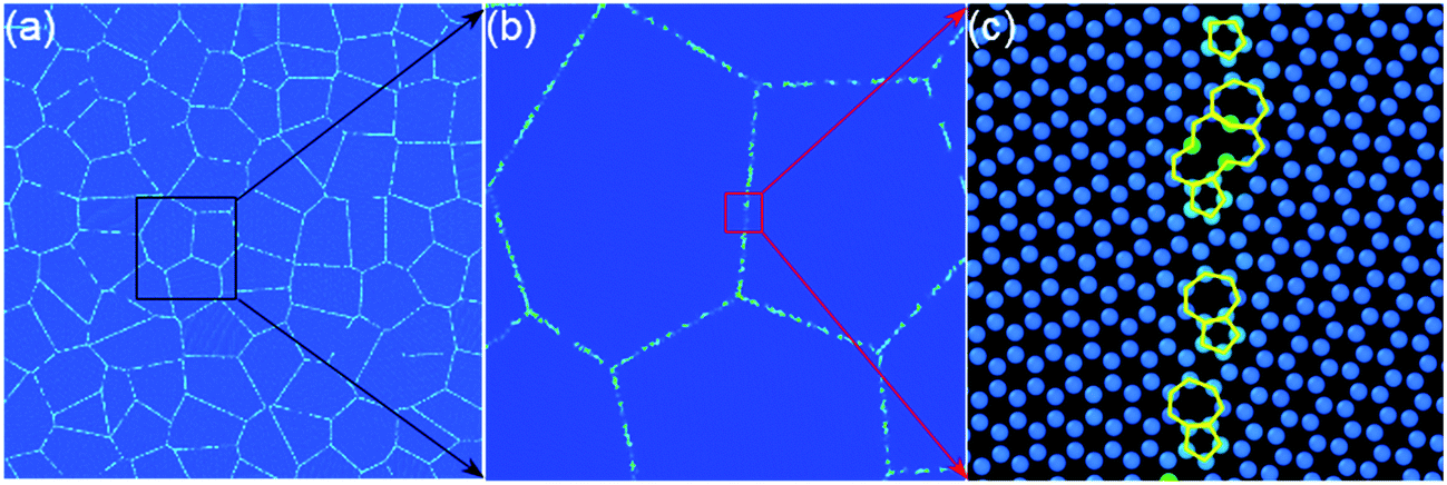 | ||
| Fig. 1 A typical polycrystalline graphene model. | ||
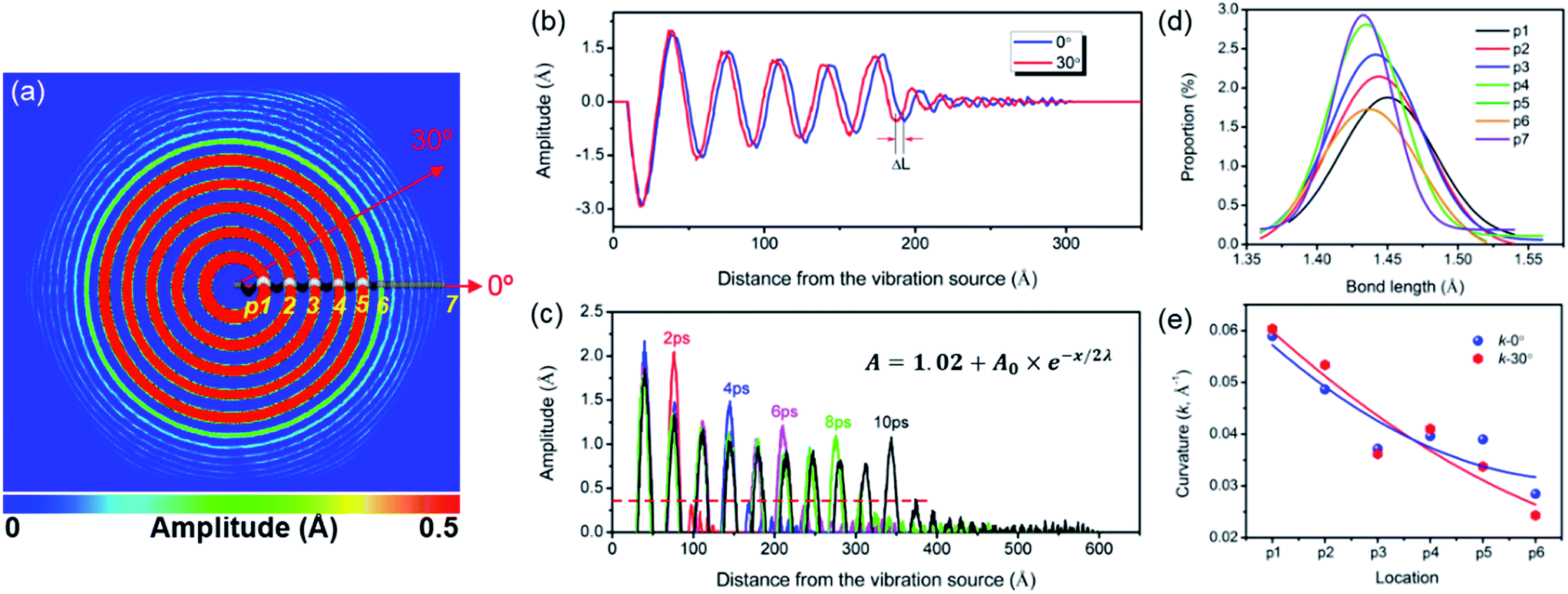 | ||
| Fig. 2 (a) A hexagonal vibration wave pattern, (b) the vibration amplitudes along ZZ and AC directions, (c) the displacement of the wave front along AC directions as a function of time, (d) the bond length distributions and (e) the bending curvatures of Points 1–6 in panel (a). | ||
The simulation is carried out using the package LAMMPS. The interactions between carbon atoms are described by the AIREBO potential, which can accurately capture the interaction between carbon atoms as well as bond breaking and bond reforming.29 The cutoff parameter describing the short-range C–C interaction is selected to be 2.0 Å in order to avoid spuriously high bond forces and nonphysical results at large deformation.30 The Nose'e–Hoover thermostat is utilized to account for the thermal effect. The vibration source moves in an oscillatory fashion, so that the amplitude at the time t A(t) is given in vector notation as: A(t) = A0 × sin(2πt/T) A0 is the specified amplitude of 0.3 nm and T is the oscillation period of 1.0 ps. The interlayer separation of graphite, 3.4 Å, is taken as the effective thickness of the monolayer graphene. Prior to loading, the polycrystalline graphene sheets are fully relaxed to an equilibrium state in the isothermal–isobaric ensembles at 300 K for 20 ps. The time step of 1 fs is adopted in the MD simulation and for each step.
3. Results and discussions
3.1 Vibration characteristics in single-crystal graphene
Fig. 2 displays the mechanical wave propagation in single-crystal graphene sheet and it is colored according to the out-of-plane displacement. The vibration ripple morphology is a circle in the central region, characteristic of isotropic propagation but becomes a hexagon pattern at the wave front, characteristic of anisotropic propagation. Fig. 1(a) shows the enlarged hexagonal region at 6 ps. The zigzag (ZZ, 0°) and armchair (AC, 30°) directions are denoted by the red arrows. The displacement profiles along z axis are extracted, and the results are shown in Fig. 2(b). The curves become separated from each other gradually with increasing distance from the vibration source, confirming different phase velocities. Clearly, the propagation velocity along the ZZ direction is faster than that along the AC direction by 8.3%. This results in the ripples in hexagonal symmetry rather than in circle pattern. Similar results were observed by Wu et al.31 Fig. 2(c) shows the vibration profile along ZZ direction at different times. The out-of-plane movement is damping and the damped amplitude can be fitted by , in which x is the distance from the vibration source, A0 is the amplitude at the vibration source, λ is the propagation wave length. The fitted values for y0, A0 and λ are 1.02, 2.92 Å and 32.45 Å, while these for the AC direction are 0.96, 2.72 Å and 38.42 Å, respectively. The damping can be attribute to the bending curvature to some extend.32 The amplitude profile is fitted with a sinusoidal function, and the curvatures at Points 1–7 are presented in Fig. 2(e). When the distance from vibration source is larger than a critical value (at Point 6), the difference of curvature along ZZ and AC directions becomes more and more considerable. For instance, the curvature at Point 6 along AC direction is much smaller than that along ZZ direction. The flexural response of graphene sheet of small size cannot be accurately described by the classical Euler regime, and preferential buckling occurs along ZZ direction owing to the non-continuum effect. As the buckling range increases, wrinkles dominate the morphology of monolayer graphene.33
Thermodynamically, the large-amplitude wave cannot propagate far away from the vibration source, unless energy is continuously supplied. Ripples emerge on the graphene layers during dynamic loading, while part of them disappear during unloading, and the energy is partially absorbed. The absorption of vibration energy is related to bond length variation, bond angle adjustment and dihedral angle change. Fig. 2(d) shows the bond length distribution at Points 1–7. Apparently, the bonds at the vibration source are substantially elongated, and the bond length decreases with increasing distance from the vibration source by 1.2%. This results in damping wave, and the wave amplitude decreases with increasing distance from the vibration source. Lahiri et al. also observed ripples in monolayer graphene,34 and the ripples commonly lead to the damping behavior of waves in graphene membrane.
3.2 Vibration propagation in polycrystalline graphene
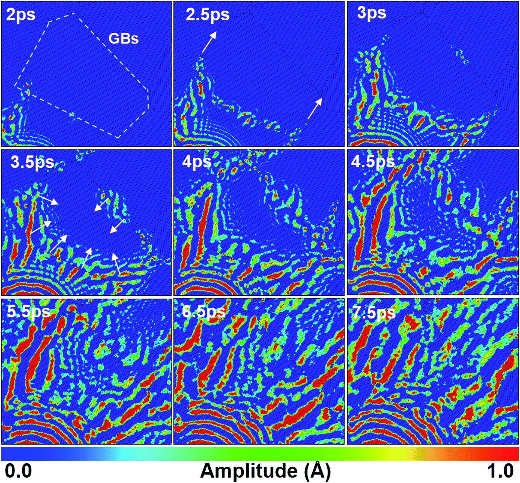
The influences of GBs in a polycrystalline graphene sheets on the vibration wave propagation are studied in this section. Fig. 3(a) shows the oscillation mode and the evolution of vibration wave as a function of time. The double arrow in Fig. 3(b) shows the position of the vibration source. The amplitude profile along the white dot line is plotted in the red curve at the bottom of the panel. Fig. 3(c) shows the wave morphology evolution at different times. Interestingly, the vibration features in the polycrystalline graphene sheets are completely different from that in the single-crystal graphene. The circular ripple can hardly move across the GBs. The front of the vibration wave is no longer a regular hexagon or a circle at all, and any sinusoidal-like wave propagation cannot be identified. The vibration amplitude in GBs is much larger than that in grains, indicating stronger vibration at GBs. Under the same condition, the phase velocity in polycrystalline graphene sheet (133.3 Å ps−1) is more than two times that in single-crystal graphene sheet (58.7 Å ps−1). As shown in Fig. 3(d), the atoms in GBs act as the second-generation vibration source (2nd-gVS). This results in circular ripples around the defects. The ripples can spread out for several nanometers. The wave morphology changes due to diffraction at vacancies. When the wave arrives at the vacancies, the smooth circle ripples induce a small crater or even be separated into two parts, dependent on the size and shape of vacancies. At high vacancy density, the circle ripples become quite rough, and interference takes place when two diffraction waves are encountered in the same grain.35 Consequently, the wave propagation pattern can not only be adopted to distinguish the GBs, but also be used to identify the locations and sizes of the defects in GBs. For example, the contour lines of GBs might be depicted by analyzing the 2nd-gVSs distribution, as shown by the white dot lines in Fig. 2(d). Furthermore, the strain field can be estimated by comparing the relative radius of the circular ripples around the 2nd-gVSs. As marked by two yellow lines in Fig. 3(a), the outward propagation from the 2nd-gVSs α is squeezed by two neighbors. Ideally, the circular ripple around the 2nd-gVS at GBs is composed of two arc-shaped segments, but at least three arc-shaped segments at triple-junction. Based on the different propagation velocity along ZZ and AC directions, the grain orientation can also be analyzed from the wave propagation patterns. | ||
| Fig. 3 (a) Oscillatory fashion of the moving vibration source indicated as the double arrow in (b), (b) a vibration profile on polycrystalline graphene sheet at 6 ps, the red curve below shows the vibration amplitude profile along the write dot line, (c) the vibration wave propagation at different times, and (d) a distribution of the second-generation vibration sources (2nd-gVSs). | ||
The wave propagation in polycrystalline graphene is isotropic as a whole because of randomly distributed grains. But it is anisotropic in local regions. The propagation velocity in GBs is faster than that in grain domains. Essentially, GBs are composed of topological defects and disordered atomic configurations without any symmetry, characteristics of an amorphous state. Moreover, GBs have a lower mass density.36,37 The phase velocity is related to the mass density as
 | (1) |
 | ||
| Fig. 4 Snapshots of the vibration wave propagating near GBs. | ||
The amplitude at GBs, triple-junctions (TRI-J) and grain domains (GDs) on the red circle in Fig. 5(a) are recorded, and Fig. 5(b) displays the result as a function of times. Before 2 ps, the vibration amplitudes at GBs, TRI-J and GDs are almost the same. After 3 ps, the vibration amplitudes at GBs and TRI-J become substantial, and are much larger than that at GDs. Fig. 5(c) displays a snapshot of the vibration configuration at 7 ps. The amplitude is radially distributed and significantly enhanced at GBs. Fig. 5(d) shows the amplitude profile along the black circle. Different from the smooth amplitude profile in single-crystal graphene sheet, it is burr shaped in polycrystalline graphene sheet, which is related to the radial pattern.
 | ||
| Fig. 5 (a) Three typical points on a circle, (b) the amplitudes at GBs, TRI-J and GDs, (c) the wave profile at 7 ps, (d) the amplitude profile along the black circle in single-crystal graphene sheet (S-GS) and in polycrystalline graphene sheet (P-GS). | ||
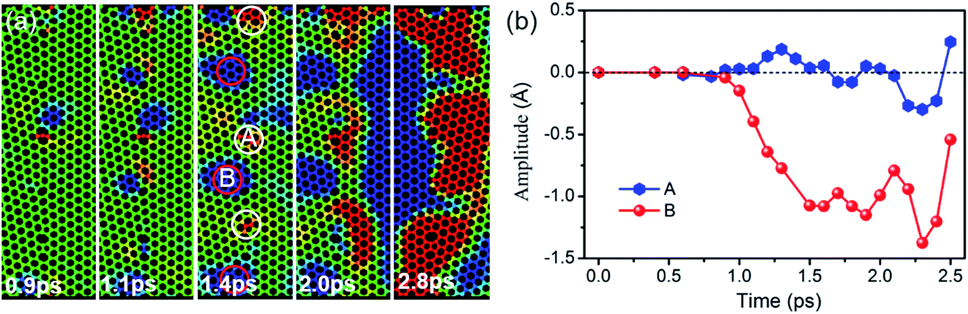
To further understand the effect of GBs on terahertz wave propagation, a piece of grain boundary is magnified and shown Fig. 6(a). At the beginning, the relaxed grain boundary is almost smooth as a plane, but it is metastable and out-of-plane protuberance and depression emerge under a perturbation, resulting in intrinsic ripples, particularly, at GBs. The number of the intrinsic ripples increases gradually. The red circle is used to indicate downward movement with respect to the plane of z = 0, while the white circle is adopted to indicate upward displacement. When the vibration ripples arrive at, the interference will take place between the vibration ripple and the intrinsic ripple. The amplitude is increased at Point A, but is reduced at Point B. Fig. 6(b) shows the amplitudes at Points A and B as a function of time. A large height perturbation of 1.2 Å is evidenced between Points A and B at 1.4 ps, which is consistent with the reported results.39,40 When the wave moves across the GB, Points A and B move up and down as the rhythm of the vibration source. So, the vibration ripples might destabilize the thermal stability of graphene sheets and thus change the morphologies of intrinsic ripples. Public reports demonstrate that the finite element approach yields considerably close thermal conductivity to the equilibrium molecular dynamics estimations for the entire range of studied grain sizes, and decreasing the grain size decreases the thermal conductivity due to phonon scattering at the grain boundaries.41 Chowdhury finds that the vibrational frequencies obtained from the simple continuum plate model are comparable to the vibrational frequencies computed using the molecular mechanics approach (MM), but the continuum model tends to overestimate the MM predictions for smaller grains because of the isotropic assumption.42 Totally speaking, for sample with small grain size, reliable result can be obtained using MDs; for sample with large grain size, MDs result have a similar accuracy with FET result except that MDs can also show the configuration evolution of the grain boundaries. Hence, our methods and the conclusions can be extended to simulate the vibration wave propagation in large scale grains to some extent.
 | ||
| Fig. 6 (a) The atomic configuration evolution of the GB as a function of time, (d) the amplitude variations at Points A and B. | ||
4. Conclusions
In this paper, molecular dynamic simulations are performed to study the mechanical transverse wave in both single-crystal and polycrystalline graphene sheets. It is found that the wave propagation is isotropic in single-crystal graphene sheets at the center of the vibration pattern but becomes anisotropic at external frontiers because of orientation dependent phase velocity. The transverse wave in single-crystal graphene sheet is a damped oscillation that can be expressed as a function of the vibration source amplitude and propagation wave length. However, wave propagation in polycrystalline graphene sheet is completely isotropic as a whole and, the phase velocity in GBs is faster than that in grains, and the wave amplitude at GBs is larger than that in grains, owing to the lower mass density and the reduced bonding force in GBs. Regions with large out-of-plane displacement distribute along the GBs. It is believed that the GBs could be more capable of absorbing energy from the waves, but have less capability to spread the gained energy again. The results provide us a fundamental understanding on the mechanical vibration in graphene sheets.Acknowledgements
This work was jointly supported by National Natural Science Foundation of China (Grant No. 51471130, 51302162), Fundamental Research Funds for the Central Universities.References
- A. K. Geim and K. S. Novoselov, Nat. Mater., 2007, 6(3), 183–188 CrossRef CAS PubMed.
- Q. Lu, M. Arroyo and R. Huang, J. Phys. D: Appl. Phys., 2009, 42(10), 102002–102006 CrossRef.
- J. U. Lee, D. Yoon and H. Cheong, Nano Lett., 2012, 12(9), 4444–4448 CrossRef CAS PubMed.
- J. W. Jiang, J. S. Wang and B. W. Li, Phys. Rev. B: Condens. Matter Mater. Phys., 2009, 80(11), 113405–113414 CrossRef.
- K. Saitoh and H. Hayakawa, Phys. Rev. B: Condens. Matter Mater. Phys., 2010, 81(11), 115447–115454 CrossRef.
- J. A. Baimova, S. V. Dmitriev, K. Zhou and A. V. Savin, Phys. Rev. B: Condens. Matter Mater. Phys., 2012, 86(3), 035427–35434 CrossRef.
- Z. Y. Qian, F. Z. Liu, Y. Hui, S. Kar and M. Rinaldi, Nano Lett., 2015, 15(7), 4599–4606 CrossRef CAS PubMed.
- T. F. Miao, S. Yeom, P. Wang, B. Standley and M. Bockrath, Nano Lett., 2014, 14(6), 2982–2987 CrossRef CAS PubMed.
- A. D. Smith, F. Niklaus, A. Paussa, S. Schroder, A. C. Fischer and M. Sterner, et al., ACS Nano, 2016, 10(11), 9879–9888 CrossRef CAS PubMed.
- M. K. H. Bhaskaran, Nano Lett., 2015, 15(4), 2562–2567 CrossRef PubMed.
- S. Poperezhai, P. Gogoi, N. Zubenko, K. Kutko, V. Kutko and A. Kovalev, et al., J. Phys.: Condens. Matter, 2017, 29(9), 095402–095409 CrossRef CAS PubMed.
- C. Y. Chen and J. Hone, Proc. IEEE, 2013, 101(7), 1766–1814 CrossRef CAS.
- M. G. Chung, D. H. Kim, D. K. Seo, T. Kim, H. U. Im and H. M. Lee, et al., Sens. Actuators, B, 2012, 169, 387–396 CrossRef CAS.
- G. S. Kulkarni, K. Reddy, Z. Zhong and X. Fan, Nat. Commun., 2014, 5, 4376–4377 CAS.
- P. Li, B. Zhang and T. Cui, Biosens. Bioelectron., 2015, 72, 168–177 CrossRef CAS PubMed.
- J. Atalaya, A. Isacsson and J. M. Kinaret, Nano Lett., 2008, 8(12), 4196–4205 CrossRef CAS PubMed.
- K. Iyakutti, V. J. Surya, K. Emelda and Y. Kawazoe, Comput. Mater. Sci., 2012, 51(1), 96–97 CrossRef CAS.
- V. K. Tewary, Phys. Rev. B: Condens. Matter Mater. Phys., 2009, 80(16), 161409–161414 CrossRef.
- E. Mahmoudinezhad and R. Ansari, Phys. E, 2013, 47, 12–16 CrossRef CAS.
- T. R. Albrecht, H. A. Mizes, J. Nogami, S. I. Park and C. F. Quate, Appl. Phys. Lett., 1988, 52(5), 362–364 CrossRef CAS.
- W. Regan, N. Alem, B. Aleman, B. S. Geng, C. Girit and L. Maserati, et al., Appl. Phys. Lett., 2010, 96(11), 113102–113104 CrossRef.
- Z. L. Li, Z. M. Li, H. Y. Cao, J. H. Yang, Q. Shu and Y. Y. Zhang, et al., Nanoscale, 2014, 6(8), 4309–4317 RSC.
- P. Yasaei, B. Kumar, R. Hantehzadeh, M. Kayyalha, A. Baskin and N. Repnin, et al., Nat. Commun., 2014, 5, 1–8 Search PubMed.
- B. Wang, Y. Puzyrev and S. T. Pantelides, Carbon, 2011, 49(12), 3983–3986 CrossRef CAS.
- Y. N. Dong, Y. Z. He, Y. Wang and H. Li, Carbon, 2014, 68, 742–746 CrossRef CAS.
- W. Z. Bao, F. Miao, Z. Chen, H. Zhang, W. Y. Jang and C. Dames, et al., Nat. Nanotechnol., 2009, 4(9), 562–565 CrossRef CAS PubMed.
- D. B. Zhang, E. Akatyeva and T. Dumitrica, Phys. Rev. Lett., 2011, 106(25), 255503–255504 CrossRef PubMed.
- J. Kotakoski and J. C. Meyer, Phys. Rev. B: Condens. Matter Mater. Phys., 2012, 85(19), 195447–195455 CrossRef.
- D. W. Brenner, O. A. Shenderova, J. A. Harrison, S. J. Stuart, B. Ni and S. B. Sinnott, J. Phys.: Condens. Matter, 2002, 14(4), 783–820 CrossRef CAS.
- O. A. Shenderova, D. W. Brenner, A. Omeltchenko, X. Su and L. H. Yang, Phys. Rev. B: Condens. Matter Mater. Phys., 2000, 61(6), 3877–3912 CrossRef CAS.
- X. Liu, F. Wang and H. Wu, Appl. Phys. Lett., 2013, 103(7), 071904–071905 CrossRef.
- T. Ma, B. Li and T. Chang, Appl. Phys. Lett., 2011, 99(20), 201901–201904 CrossRef.
- X. Y. Liu, F. C. Wang and H. A. Wu, Nanotechnology, 2015, 26(6), 065701–065709 CrossRef CAS PubMed.
- D. Lahiri, S. Das, W. B. Choi and A. Agarwal, ACS Nano, 2012, 6(5), 3992–3999 CrossRef CAS PubMed.
- Y. Z. He, H. Li, P. C. Si, Y. F. Li, H. Q. Yu and X. Q. Zhang, et al., Appl. Phys. Lett., 2011, 98(6), 063101–063104 Search PubMed.
- S. Malola, H. Hakkinen and P. Koskinen, Phys. Rev. B: Condens. Matter Mater. Phys., 2010, 81(16), 165447–165454 CrossRef.
- Z. Yang, Y. H. Huang, F. Ma, Y. J. Sun, K. W. Xu and P. K. Chu, Mater. Sci. Eng., B, 2015, 198, 95–97 CrossRef CAS.
- Z. Yang, Y. H. Huang, F. Ma, Y. P. Miao, H. W. Bao, K. W. Xu and P. K. Chu, RSC Adv., 2016, 6(65), 60856–60866 RSC.
- O. V. Yazyev and S. G. Louie, Phys. Rev. B: Condens. Matter Mater. Phys., 2010, 81(19), 195420–195424 CrossRef.
- Y. Y. Liu and B. I. Yakobson, Nano Lett., 2010, 10(6), 2178–2186 CrossRef CAS PubMed.
- B. Mortazavi, M. Pötschke and G. Cuniberti, Nanoscale, 2014, 6(6), 3344–3349 RSC.
- R. Chowdhury, S. Adhikari, F. Scarpa and M. I. Friswell, J. Phys. D: Appl. Phys., 2011, 44(20), 205401–205411 CrossRef.
| This journal is © The Royal Society of Chemistry 2017 |