DOI:
10.1039/C7RA03732E
(Paper)
RSC Adv., 2017,
7, 31989-31996
Induced alignment of a reactive mesogen-based polymer electrolyte for dye-sensitised solar cells
Received
31st March 2017
, Accepted 16th June 2017
First published on 22nd June 2017
Abstract
Liquid crystalline materials are interesting organic molecules possessing anisotropic behaviour. The materials undergo self-assembly forming highly ordered structures, which from the opto-electronic applications point of view, have a promising future. By controlling the functionality or the mesophase of the liquid crystal materials, it is possible to develop specific device architectures. So far, controlling the morphologies of organic materials for electronic applications has proven to be difficult. Here, we prepared a liquid crystal-based polymer template using a polymer alignment layer and electric field. The resultant morphology is closely related to the fabrication technique which can be further modified to suit particular device applications. The mesophase characteristics and morphologies of these materials are characterised using polarising optical microscopy, atomic force microscopy and scanning electron microscopy. Next, we utilised these polymer electrolytes in dye-sensitised solar cells as a potential application. Device performance such as open-circuit voltage, short-circuit current, fill-factor and power conversion efficiencies also showed strong dependence on the structure of the polymer scaffold. Hierarchical polymer electrolyte structures were prepared using a reactive mesogen assisted by Smectic A liquid crystals. The morphology of these hierarchical structures was controlled by the use of alignment layers on the substrate or by applying electric fields. The highest power conversion efficiency achieved was 5.02% in cells with electric field induced alignment, as compared to 4.57% for the polyimide aligned sample. This can be attributed to the higher porosity in the case of the electric field aligned sample whereas for the polyimide aligned sample, despite having more ordered pores, the width between the pores is comparatively smaller.
Introduction
The self-assembly of LC materials into ordered morphologies is very promising for device applications.1 This is typically achieved through weak inter-molecular interactions between molecules to create complex structures. The typical methods to control these weak interactions are through the use of a variety of different molecular compounds which are able to form phase-segregated structures.2 The self-assembly of LCs is achieved naturally either due to hydrogen bonding, dispersive forces, and in some cases π–π stacking of the molecules.3,4 These add functionality to the original material. In addition to self-assembly, LC materials also respond to the application of external electric (E) or magnetic (H) fields due to the presence of polar groups in the molecular structure.5 Typically, the presence of a periphery polar group to the core or the end chain of the molecule causes polarisation of the overall molecule. This polarisation allows alignment of the molecule in response to the applied field as part of an energy minimisation process. In addition to this, the morphology of the LC can also be controlled by using a thin alignment layer on the substrate of the LC device.6 A thin layer of polymer which has been rubbed in one direction is employed where the LC molecules align in the grooves produced by the rubbing action.7 By taking full advantage of this effect, it is possible to control the structure of LCs to suit particular applications. These characteristics allows researchers to manipulate the LC mesophase for use in a wide range of applications including displays, lasers, solar cells and many more.8–10
Smectic LCs are an interesting class of LC materials which have higher order (positional as well as orientational) as compared to the nematic LCs,11 in the sense that in additional to orientational order characteristic of nematics, they also possess positional order in terms of layering of the LC director. In Smectic A LCs, the LC director is aligned perpendicular to the Smectic layers, whilst in Smectic C LCs, the director is oriented at a tilted angle with respect to the Smectic layers. Typically, the Smectic LC phase is obtained with molecules having non-polar aromatic cores with two alkyl side chains or even with one alkyl chain provided that the alkyl chain is long enough to provide separation.12 This separation allows the Smectic LC phase to form a lamellar structure which is due to chemical compatibility. This segregation is driven by molecules showing amphiphilic behaviour such as in the case of organosiloxane and hydrocarbon.13 This potential for segregation coupled with its higher positional order enables the Smectic LC to act as a templating material. In this case, the Smectic LCs can exert higher influence over the morphology of the materials to be synthesised. The synthesised materials are expected to replicate the structure of the Smectic LCs, which self-assemble into repeat units of the dimensions of several nanometres.
In organic electronics, controlling the morphology and structure of the organic compounds is essential in realising high efficiency devices such as organic field effect transistors and organic solar cells.14 The objective of controlling the morphology is to improve the interface characteristics between the electron donor and acceptor for efficient exciton dissociations, as in the case of organic solar cells. Some of the methods employed to control the morphology and molecular packing include thermal annealing, solvent annealing, choice of solvents and additives.15–18 Cho et al. showed the transition of the morphology of the polyelectrolyte from nano-porous to micro-porous after applying E.19
In addition to organic solar cells, dye sensitised solar cells (DSSCs) are an organic inorganic hybrid that are promising candidates for low-cost photovoltaic applications at relatively high efficiencies.20 However, solvent evaporation and leakage of liquid electrolyte-based DSSCs make the commercialisation of DSSCs difficult.21 To address this issue, solid state and quasi-solid state polymer electrolyte has been suggested as the alternative.22,23 Despite showing a relative increase in device stability, a lot of these approaches lead to device efficiencies that are lower than that of liquid electrolyte-based DSSCs. This is because the polymer network has been found to impede the ionic conduction which leads to low ionic conductivity.24 Highly ordered ionic conduction pathways have been proposed as a possible method to mitigate conductivity problems and researches are now looking to employ nanostructures in the DSSCs.25,26
In this work, we prepared a mixture of an optimised NLC![[thin space (1/6-em)]](https://www.rsc.org/images/entities/char_2009.gif) :Smectic A (SmA) binary LC mixture, a reactive mesogen and a photoinitiator based on previous literature.27 As an extension of the idea of self-assembled LC-templated material, we have used applied E and PI alignment layer to control the structure of the LC mixture. It is demonstrated that the morphology of these LC-templated materials are related to their electrical and electrochemical properties. A potential application of these templated materials is demonstrated through the fabrication and characterisation of DSSCs. It is proposed that this work will allow better understanding of the interaction between LCs and external conditions.
:Smectic A (SmA) binary LC mixture, a reactive mesogen and a photoinitiator based on previous literature.27 As an extension of the idea of self-assembled LC-templated material, we have used applied E and PI alignment layer to control the structure of the LC mixture. It is demonstrated that the morphology of these LC-templated materials are related to their electrical and electrochemical properties. A potential application of these templated materials is demonstrated through the fabrication and characterisation of DSSCs. It is proposed that this work will allow better understanding of the interaction between LCs and external conditions.
Experimental
Materials
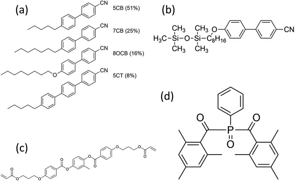
E7 LC was received from Merck. Lithium iodide (LiI), iodine (I2) and 4-tert-butylpyridine (TBP) were purchased from Sigma-Aldrich. Ti-nanoxide D/SP paste, 1,2-dimethyl-3-propylimidazolium iodide (DMPII) and meltonix 1170-25 (DuPont Surlyn®) were purchased from Solaronix. Di-tetrabutylammonium cis-bis(isothiocyanato)bis(2,2′-bipyridyl-4,4′-dicarboxylato)ruthenium(II) (N719) dye was received from Organica®. RM257 and IR819 were obtained from Merck. All materials were used as received without further purification. 8/2 organosiloxane has been synthesised in house according to previous work.28
Methods
Liquid crystal binary mixture preparation
LC mixtures of SmA (8/2 organosiloxane) and NLC (E7) were prepared with a 20:80 ratio by weight. The binary LC mixture was then mixed with a reactive mesogen (RM257) and a photoinitiator (IR819). The mixture was heated in an oven above the isotropic temperature for 4 hours. After that, the mixture was filled into a cell with a thickness of 15 μm and cured using a UV light (1 mW cm−2) for 1 min. The structures of the materials are shown in Fig. 1.
 |
| | Fig. 1 Chemical structure of (a) nematic E7, (b) Smectic 8/2 organosiloxane, (c) the reactive mesogen, RM257 and (d) the photoinitiator, IR819. | |
Substrates preparation
In order to fabricate the ordered Smectic template, a cell was fabricated with platinum-coated fluorine-doped tin oxide (FTO) substrate on one side and polyvinyl alcohol (PVA)-coated glass substrate on the other side. The FTO substrates were spin-coated with platinum paste (Dyesol's PT1 Platinum Paste) at 2000 rpm for 60 s and annealed at 450 °C for 30 min. The PVA layer on the other substrate acts as a sacrificial layer so that it is easy to crack open the cell afterwards. Once the mixture has been polymerised, the LC component was removed by immersing the cell in acetone for 24 hours. The cell was then opened leaving the nanochannel template on the platinum side. This substrate was then used to fabricate DSSC.
The alignment layer is prepared using a polyimide (AL-16301) solution diluted in cyclopentanone. The alignment layer solution was spin-coated on the pre-cleaned ITO substrate at a spin speed of 3000 rpm for one minute, followed by baking at 220 °C for 30 minutes to evaporate the solvent. After cooling down the substrate to room temperature, the substrate is then rubbed using a rubbing machine which has been built in-house. The rubbing machine consisted of a rotating drum covered with a nylon cloth.
Liquid crystals switching
Switching of the LC mixture is done in 25 μm ITO-Pt-coated FTO substrate. An applied voltage of 120 V peak-to-peak at a frequency of 1 kHz was applied to the substrate using a function-generator (Thurlby Thandar Instruments TTi TG1304). The function-generator output was amplified by a voltage amplifier.
Device fabrication
The photoanodes were prepared by spin-coating a thin layer (100 nm) of compact TiO2 onto FTO substrate and annealed at 450 °C for 30 min. The spin-coated substrates were then bar-coated with titania paste (Dyesol's 18NR-T Transparent Titania Paste) and then annealed at 500 °C for 30 min. The resulting thickness was approximately 8 μm, that was verified using a contact profilometer (DEKTAK). The substrates were then immersed in 0.3 mM N719 dye solution for 24 hours. Excess dye was removed by washing the substrate with acetonitrile for several times. The photoanode and the photocathode with nanochannel template were glued together using 25 μm sealing film (Meltonix 1170-25). The electrolyte which consists of 0.6 M MPII, 0.5 LiI, 0.05 I2 and 0.5 M TBP in acetonitrile were capillary filled into the cell. The active area of the cell is controlled to be 0.283 cm2.
Characterisation
Differential scanning calorimetry (DSC) was employed to determine the transition temperature of the LC. The measurement was performed using a Mettler Toledo DSC 823e at a heating and cooling rate of 5 °C min−1 from 0 °C to 100 °C. An Olympus polarising optical microscope (POM) (BX60) attached to a programmable hot-stage was used to obtain the morphology of the LC mixtures. The samples were brought into the isotropic phase and slowly cooled down to their liquid crystal phase. All images were taken at room temperature. The heating or cooling temperature was controlled at 5 °C min−1. The ex situ characterisation of the polymer on silicon substrate was carried out using scanning electron microscopy (SEM, Zeiss SigmaVP, 2 kV) and tapping mode atomic force microscopy (AFM, Agilent 5400 SPM). The conductivity measurement was performed using a Keithley 4200-SCS parameter analyser. The measurement was performed at room temperature in a ITO–ITO cell with 25 μm thickness. J–V measurement of the solar devices was performed using Keithley sourcemeter controlled by a Labview automation program developed in-house. The measurement was performed from −1.0 to 1.0 V at 100 mW cm−2 sunlight at AM 1.5G (1 sun). Electrochemical impedance spectroscopy (EIS) and steady state voltammetry were performed on a Solartron 1260 Impedance Analyzer. For the EIS, the measurements were carried out in the frequency range of 10 mHz to 1 MHz with a 10 mV step under dark. For the steady-state voltammogram, the measurement was carried out from −1.5 V to 1.5 V at a rate of 10 mV s−1.
Results and discussion
Preparation of LC binary mixture
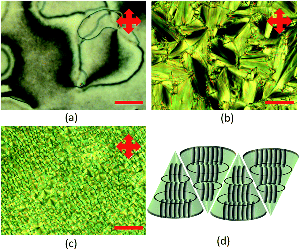
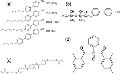
Fig. 2 shows the morphology of the LC mixtures in their LC phase. The SmA phase is characterised by the fan-shaped structure (Fig. 2a). On the other hand, E7 showed a schlieren texture which is typical for nematic liquid crystal (Fig. 2b). The addition of a nematic LC into SmA is necessary due to the difficulty in switching the SmA LCs. By using the nematic LC with high dielectric permittivity, it is possible to orientate the molecules by applying E. Without the nematic LC, a higher E is needed to fully switch the LC material. In the SmA:E7 20:80 mixture, an interesting texture could be seen (Fig. 2c). The structure showed standing columns of an even diameter which means that the focal conic structures were lying vertically, showing a polygonal texture. Fig. 2d shows the schematic diagram of SmA LCs where the molecules formed focal conic structures originating from molecules from different layers of LC molecules.
 |
| | Fig. 2 POM images of (a) pure E7, (b) pure SmA, (c) binary LC mixture and (d) schematic diagram of the polygonal structure formed by the binary LC mixture (side view). The scale bar is 50 μm using ×60 magnification. | |
Preparation of LC template
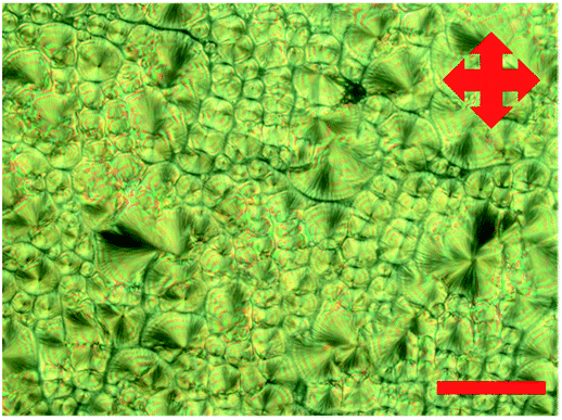
Next, to prepare the liquid crystal template, RM 257 and IR 819 were added to the liquid crystal mixture. A slight change could be observed after the addition of the two components. Instead of showing well-defined columns, the structure showed micron-sized platelets. Fig. 3 shows the formation of the micron-sized platelets of the LC template before polymerisation. This could mean that the order that was obtained previously has been disrupted by the extra components. A detailed discussion on the formation of the self-assembled LC template has been discussed in our previous work.27
 |
| | Fig. 3 POM images of reactive mesogen mixtures before polymerisation. The scale bar is 50 μm using ×60 magnification. | |
Preparation of LC template using E
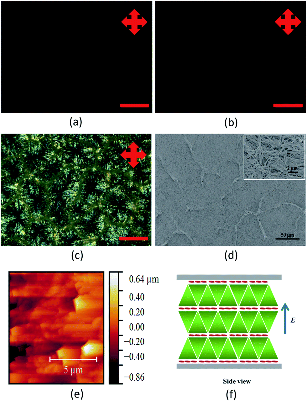
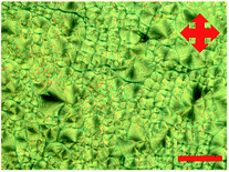
Fig. 4 shows the POM and SEM of the E aligned sample. The binary LC mixture showed a marked difference after applying the electric field which indicates that the LC materials have been switched. For typical nematic LCs, the realignment of the directors of the LC molecules changed the optical transmission of the sample, which is characterised by an opaque texture. The molecules are thought to be aligned parallel to the applied E and thus allowing light to pass through. However, this is not the case here. Applying E induces an overall planar alignment of the LC molecules which is clearly evident from the POM images. Initially, before applying E, an intermediate alignment of the LC molecules that consist of both planar and homeotropic components can be seen with the formation of polygonal structures interspersed with fan-shape structures. After applying E, the morphology changed drastically showing a dark image which means that the molecules have realigned into a planar orientation with respect to the plane of the substrates (Fig. 4a). This can be attributed to the more stable SmA LC 8/2 organosiloxane which could not be switched by the applied E but only the more fluid-like nematic 5CB molecules are aligned by the applied E. Once the sample is switched, the structure remains in that state indefinitely after the removal of the field. The sample was subsequently polymerised under UV light. The resulting texture was the same as before polymerisation (Fig. 4b). Immersing the polymerised sample in acetone removes the LC components resulted in the formation of nanopores (Fig. 4c). Fig. 4d shows the SEM image of the LC template after the removal of the LC content. Fig. 4e corresponds to the AFM image of the sample. The side view schematic diagram of the template upon applying E field is given in Fig. 4f. It is thought that the focal conic structures formed layers with the reactive mesogens situated in between these layers.
 |
| | Fig. 4 POM images of reactive mesogen mixtures after applying an out-of-plane electric field, E, (a) before polymerisation, (b) after polymerisation and (c) after removal of LC components with acetone. (d) SEM image and (e) AFM image of the template. (f) Schematic diagram of the mixture after applying E. The scale bar is 50 μm using ×60 magnification. | |
Preparation of LC template using PI alignment layer
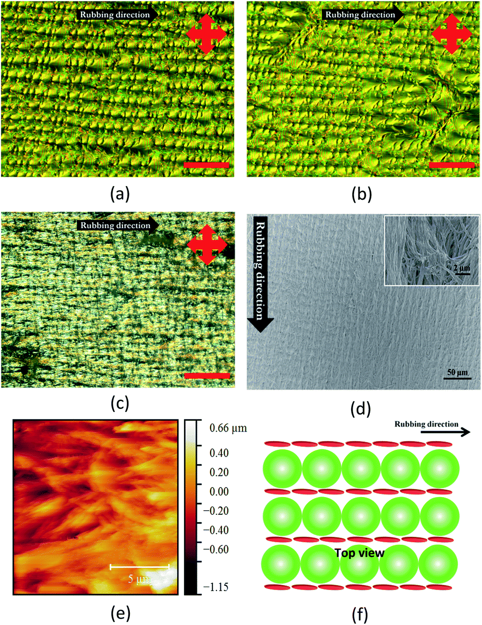
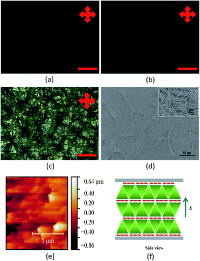
Next, an alignment layer was used on one side of the cell. The alignment layer was prepared by spin-coating a polyimide layer and rubbed using a rubbing machine. This process lead to the formation of micro-grooves where the LC will align according to the direction of the grooves. After filling with the binary mixture, a different morphology could be observed where the polygonal structures arranged themselves in the direction of the PI alignment layers, instead of randomly as in the case of the self-assembled sample (Fig. 5a). The size of these polygonal structures are also found to be similar. This can be explained through the micro-grooves prepared from the rubbing machine which is thought to have same width. Even after UV polymerisation of the sample, no visual change was observed (Fig. 5b). After the removal of the LC components, the morphology of the sample changed significantly where the polygonal structures could no longer be observed (Fig. 5c). However, the alignment of the polymer materials can still be observed. Unlike the self-assembled sample, there pores are extremely small which means that the polymer are closely packed and dense. Similar morphology is observed under SEM where the polymers are lying parallel to the substrate and are aligned in one direction (Fig. 5d). The inset picture shows the fibrous aggregates. (Fig. 5e) shows the AFM image of the template after the removal of the LC components. (Fig. 5f) shows the top view schematic diagram of the mixture when aligned using PI alignment layer. In this case, it is hypothesised that the polygonal structures of SmA LCs arranged themselves in the rubbing direction with the reactive mesogens align in between the polygonal structures and parallel to the rubbing direction.
 |
| | Fig. 5 POM images of reactive mesogen mixtures with PI alignment layer (a) before polymerisation, (b) after polymerisation and (c) after removal of LC components with acetone. (d) SEM image and (e) AFM image of the template. (f) Schematic diagram of the mixture using PI alignment layer from top view where the polygonal structures are separated by the reactive mesogens. The scale bar is 50 μm using ×60 magnification. The black arrow shows the rubbing direction. | |
Current–voltage measurement
The effect on ionic conductivity of the different structure was studied using current–voltage measurement where the measurements were performed at room temperature. The conductivity of the LC-polymer electrolyte composite was obtained using the following equation, σ = l/RbA, where l is the thickness of the cell, Rb is the resistance and A is the overlap area of the cell. From the I–V measurement, it was found out that the ionic conductivity is higher in the case of E aligned sample (1.78 × 10⁻³ S m−1) compared to the PI aligned sample (1.49 × 10⁻³ S m−1). The highly ordered sample induced a better ionic conduction within the nano-pores by having a greater number of ionic channels. The ionic diffusion of the sample was also investigated using the steady state voltammetry. The ionic diffusion constant was obtained from the limiting current density using the linear sweep voltammogram. The diffusion coefficient can be calculated using the following eqn (1)| |
 | (1) |
where n is the electron number per molecule, F is the Faraday constant, DI3− is the diffusion coefficient of the limiting compound, cI3− is the concentration of the limiting compound, l is the thickness if the cell.29 The ionic diffusion experiments also corroborate the ionic conductivity data where E aligned sample (3.54 × 10⁻⁷ cm2 s−1) has a higher ionic diffusion in contrast to PI aligned sample (3.23 × 10⁻⁷ cm2 s−1). Similar result has also been observed by Golodnitsky et al. where their findings showed that an improvement in the ionic conductivity was obtained when the magnetic field was applied to polyethylene oxide polymer electrolyte.30 The result is also strengthened with the ionic diffusion data. Table 1 summarises the ionic diffusion and conductivity for the two different electrolytes.
Table 1 Ionic diffusion and conductivity data of E aligned sample and PI aligned sample
| Sample |
Ionic diffusion (cm2 s−1) |
Ionic conductivity (S m−1) |
| E aligned |
3.54 × 10⁻⁷ |
1.78 × 10⁻³ |
| PI aligned |
3.23 × 10⁻⁷ |
1.49 × 10⁻³ |
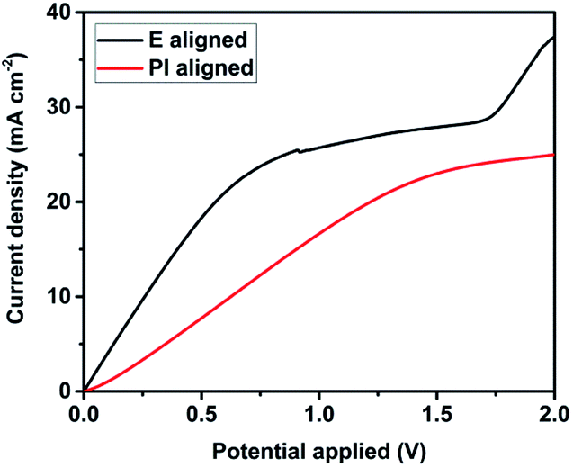
Fig. 6 shows the linear sweep voltammetry for electric field, E aligned and PI aligned samples. The ionic diffusion coefficient of the samples was calculated to be 3.54 × 10⁻⁷ cm2 s−1 for E aligned sample and 3.23 × 10⁻⁷ cm2 s−1 for PI aligned sample. The ionic diffusion coefficient for E aligned sample is slightly higher than the PI aligned sample. It is proposed that this is due to the higher porosity of the E aligned sample, hence the ionic transport is better than the PI aligned sample.
 |
| | Fig. 6 Linear sweep voltammetry curve of E aligned sample and PI aligned sample. | |
Photovoltaic properties
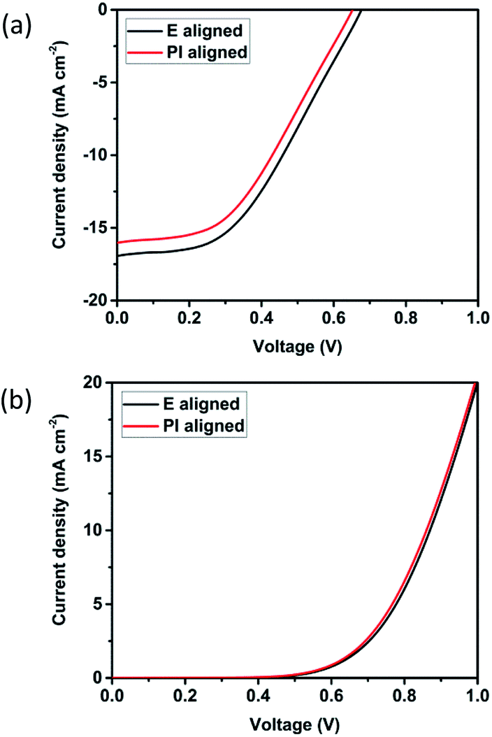
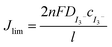
Subsequently, DSSCs were fabricated using the three different types of LC-directed self-assembled polymer templates. The J–V curves of the two different devices is shown in Fig. 7 and the measured photovoltaic parameters of the two devices are summarised in Table 2. The electric field, E aligned sample showed a JSC = 16.93 mA cm−2, VOC = 0.68 V and FF of 43.73%, corresponding to an efficiency of 5.02%. On the other hand, the performance obtained with the cell prepared using PI alignment layer was JSC = 16.03 mA cm−2, VOC = 0.65 V and a fill factor of 43.73%, corresponding to an efficiency of 4.57%.
 |
| | Fig. 7 (a) Light and (b) dark J–V of the best performing solar devices for E aligned sample and PI aligned sample. Plotted based on the best performing device for each type. | |
Table 2 Photovoltaic properties of DSSC devices prepared using E aligned and PI aligned sample. The value is the average of 4 different samples and the value for the best performing is given in the bracket
| Sample |
JSC (mA cm−2) |
VOC (V) |
FF (%) |
η (%) |
| E aligned |
13.61 (16.93) |
0.69 (0.68) |
47.10 (43.73) |
4.35 (5.02) |
| PI aligned |
13.29 (16.03) |
0.68 (0.65) |
48.41 (43.73) |
4.23 (4.57) |
As can be seen from Table 2, apart from the JSC, all other parameters are almost similar across the two devices. This is to be expected since the materials used to fabricate the sample are the same and only the morphology is different. The JSC is highly dependent on the ionic conductivity of the sample.31 The conductivity shows how good a material is to conduct current and since the same dye is used, the number of electrons excited by the dye is the same but the flow of the current is limited by the conductivity of the electrolyte. It has been shown that the ionic conductivity for the E aligned sample is higher than the PI aligned due to the polymer structure of the sample.
Electrochemical impedance spectroscopy
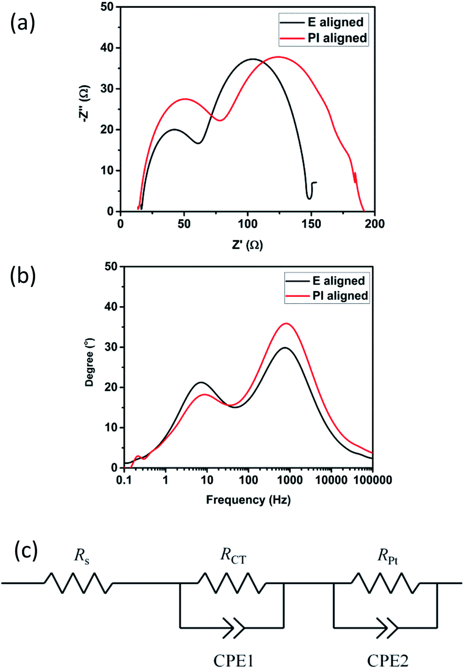
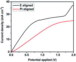
EIS provides useful information on the charge transport resistances at the interface between different components in the DSSCs.32–34 A typical Nyquist plot for the DSSC comprises of three semicircles each describing different charge transfer resistances. The first semicircle in the high frequency region can be ascribed to the charge transfer resistance at the Pt counter electrode where the intersection on the x-axis is the sheet resistance and the contact resistance, Rs of the counter electrode. The second semicircle in the medium frequency region is attributed to the RCT, charge transfer resistance at the TiO2/electrolyte interface. Lastly, the third semicircle in the low frequency region relates to the mass transport resistance in the electrolyte. Fig. 8 shows the Nyquist and Bode plot of the devices measured under dark at an applied bias of −0.7 V. The equivalent circuit for the EIS measurement is given by Fig. 8c as has been used in previous literature.35,36 The Rs for both devices are almost similar. This is as expected since they are fabricated using the same material. However, the RPt and RCT for both DSSCs show significant difference. In the case of the PI aligned device, since the width between the neighbouring polymer fibres is very small, the charge transfer from the electrode to the electrolyte is limited thus the higher RPt. This also explains why the JSC is lower in the case of PI aligned sample since the catalytic surface area is small compared to that of E aligned sample. In the case of the PI aligned device, since the width between each layer is very small, the charge transfer is limited thus the higher RPt. This also contributed to the higher RCT meaning that the electron recombination at the TiO2/electrolyte interface is greatly suppressed. Since the E aligned sample is more porous compared to the PI aligned device, the ionic transport is expected to be more efficient thus the lower RPt which agrees with the result obtained from the linear sweep voltammetry and I–V measurements. Table 3 gives the summary of the resistances and the electron lifetime.
 |
| | Fig. 8 (a) Nyquist plot and (b) Bode plot used to determine the charge transfer characteristics and electron lifetime in the two devices. (c) Equivalent circuit for the EIS measurement. | |
Table 3 Summary of EIS parameters for E aligned and PI aligned polymer electrolyte DSSCs
| Device |
Rs (Ω) |
RPt (Ω) |
RCT (Ω) |
τe (ms) |
| E aligned |
16.19 |
45.00 |
86.78 |
21.9 |
| PI aligned |
13.82 |
64.47 |
113.09 |
18.3 |
The electron lifetime can be calculated from the Bode plot using the following eqn (2)
where
fmax is the frequency of the peak in the middle frequency region.
37 The electron lifetime shows the lifetime of the electron in the TiO
2 semiconductor before recombining with the
I3− in the electrolyte. In an ideal DSSC, a longer
τe is favourable. It is calculated that the lifetime,
τe for electric field,
E aligned device (21.9 ms) is longer than that of the PI aligned device (18.3 ms). This shows that the suppression of the back recombination reaction is better in the case of the
E aligned device. The result obtained in this experiment agrees well with the result observed in the dark
J–
V.
Conclusions
New methods of preparing highly ordered LC-directed polymer-templated electrolytes have been proposed either by manipulating the self-assembly nature of LC or by applying electric fields. However, despite the more ordered structure in the case of PI aligned sample, E aligned sample showed higher ionic conductivity and thus better solar cell performance. The efficiency for the E aligned DSSC is 5.02% versus 4.57% for the PI aligned device. This can be attributed to the morphology of the polymer network where the porosity is higher in the case of E aligned sample. In the PI aligned sample, polymer fibres are relatively densely-packed with shorter inter-fibre distances, leading to lower porosity for the infiltrated liquid electrolyte. Further improvement could be attained by using NLC with higher dielectric permittivity which can allow for lower switching voltage. Additionally, the patterning of the polymer alignment layer will allow the control of the morphology of the LC template even further. The demonstration of controlling the morphology of polymer electrolyte either by using polymer alignment layer or electric fields can be applied not only in DSSCs but also in other energy storage/conversion applications including Li-ion batteries, fuel cells and capacitors.
Acknowledgements
The authors would like to thank Organica and Dyesol for providing the materials used in this experiment. A. A. K. and G. R. would like to thank the Cambridge Commonwealth European and International Trust (CCEIT). A. A. K. would also like to acknowledge the HEC (Pakistan) for financial support. E. T. would like to thank Trinity Hall, University of Cambridge for financial support. The authors would like to thank Dona Thanuja Galhena for her help in conducting the EIS experiments and Prof. Gehan Amaratunga for allowing the use of his laboratory equipment to perform the measurements.
Notes and references
- H. K. Bisoyi and S. Kumar, Chem. Soc. Rev., 2011, 40, 306–319 RSC.
- T. Kato and N. Mizoshita, Curr. Opin. Solid State Mater. Sci., 2002, 6, 579–587 CrossRef CAS.
- T. Kato, Science, 2002, 295, 2414–2418 CrossRef CAS PubMed.
- E. Pouzet, V. De Cupere, C. Heintz, J. W. Andreasen, D. W. Breiby, M. M. Nielsen, P. Viville, R. Lazzaroni, G. Gbabode and Y. H. Geerts, J. Phys. Chem. C, 2009, 113, 14398–14406 CAS.
- L. M. Blinov and V. G. Chigrinov, Electrooptic Effects in Liquid Crystal Materials, Springer, New York, 1994 Search PubMed.
- D. W. Berreman, Mol. Cryst. Liq. Cryst., 1973, 23, 215–231 CrossRef CAS.
- J. M. Geary, J. W. Goodby, A. R. Kmetz and J. S. Patel, J. Appl. Phys., 1987, 62, 4100–4108 CrossRef CAS.
- T. Uchida, Jpn. J. Appl. Phys., 2014, 53, 1–6 CrossRef.
- H. Coles and S. Morris, Nat. Photonics, 2010, 4, 676–685 CrossRef CAS.
- Q. Zheng, G. Fang, W. Bai, N. Sun, P. Qin, X. Fan, F. Cheng, L. Yuan and X. Zhao, Sol. Energy Mater. Sol. Cells, 2011, 95, 2200–2205 CrossRef CAS.
- A. Saupe, Mol. Cryst., 1969, 7, 59–74 CrossRef CAS.
- C. Tschierske, J. Mater. Chem., 1998, 8, 1485–1508 RSC.
- E. Corsellis, D. Guillon, P. Kloess and H. Coles, Liq. Cryst., 1997, 23, 235–239 CrossRef CAS.
- Y. D. Park, J. A. Lim, H. S. Lee and K. Cho, Mater. Today, 2007, 10, 46–54 CrossRef CAS.
- H. C. Liao, C. C. Ho, C. Y. Chang, M. H. Jao, S. B. Darling and W. F. Su, Mater. Today, 2013, 16, 326–336 CrossRef CAS.
- G. Shi, J. Yuan, X. Huang, Y. Lu, Z. Liu, J. Peng, G. Ding, S. Shi, J. Sun, K. Lu, H. Q. Wang and W. Ma, J. Phys. Chem. C, 2015, 119, 25298–25306 CAS.
- Z. Yi, W. Ni, Q. Zhang, M. Li, B. Kan, X. Wan and Y. Chen, J. Mater. Chem. C, 2014, 2, 7247–7255 RSC.
- Y. Chen, S. Zhang, Y. Wu and J. Hou, Adv. Mater., 2014, 26, 2744–2749 CrossRef CAS PubMed.
- C. Cho, J.-W. Jeon, J. L. Lutkenhaus and N. S. Zacharia, ACS Appl. Mater. Interfaces, 2013, 5, 4930–4936 CAS.
- B. O'Regan and M. Grätzel, Nature, 1991, 353, 737–740 CrossRef.
- M. Wang, C. Grätzel, S. M. Zakeeruddin and M. Grätzel, Energy Environ. Sci., 2012, 5, 9394 CAS.
- Z. Seidalilir, R. Malekfar, H.-P. Wu, J.-W. Shiu and E. W.-G. Diau, ACS Appl. Mater. Interfaces, 2015, 7, 12731–12739 CAS.
- G. L. De Gregorio, R. Agosta, R. Giannuzzi, F. Martina, L. De Marco, M. Manca and G. Gigli, Chem. Commun., 2012, 48, 3109 RSC.
- Z. Huo, S. Dai, C. Zhang, F. Kong, X. Fang, L. Guo, W. Liu, L. Hu, X. Pan and K. Wang, J. Phys. Chem. B, 2008, 112, 12927–12933 CrossRef CAS PubMed.
- K. Lu, J. K. Maranas and S. T. Milner, Soft Matter, 2016, 12, 3943–3954 RSC.
- D. Högberg, B. Soberats, S. Uchida, M. Yoshio, L. Kloo, H. Segawa and T. Kato, Chem. Mater., 2014, 26, 6496–6502 CrossRef.
- M. A. Kamarudin, A. A. Khan, C. Williams, G. Rughoobur, S. M. Said, S. Nosheen, A. J. Flewitt, M. M. Qasim and T. D. Wilkinson, Electrochim. Acta, 2016, 222, 657–667 CrossRef CAS.
- J. Newton, H. Coles, P. Hodgeb and J. Hannington, J. Mater. Chem., 1994, 4, 869–874 RSC.
- M. Zistler, P. Wachter, P. Wasserscheid, D. Gerhard, A. Hinsch, R. Sastrawan and H. J. Gores, Electrochim. Acta, 2006, 52, 161–169 CrossRef CAS.
- D. Golodnitsky, E. Livshits, R. Kovarsky, E. Peled, S. H. Chung, S. Suarez and S. G. Greenbaum, Electrochem. Solid-State Lett., 2004, 7, A412 CrossRef CAS.
- D. Song, W. Cho, J. H. Lee and Y. S. Kang, J. Phys. Chem. Lett., 2014, 5, 1249–1258 CrossRef CAS PubMed.
- C. Zhang, Y. Xie, T. Bai, J. Hu and J. Wang, J. Power Sources, 2015, 297, 16–22 CrossRef CAS.
- W. Yang, Y. Hao, P. Ghamgosar and G. Boschloo, Electrochim. Acta, 2016, 213, 879–886 CrossRef CAS.
- Q. Wang, J.-E. Moser and M. Grätzel, J. Phys. Chem. B, 2005, 109, 14945–14953 CrossRef CAS PubMed.
- S. Ahmed, A. Du Pasquier, T. Asefa and D. P. Birnie, Adv. Energy Mater., 2011, 1, 879–887 CrossRef CAS.
- J. Xu, S. Wu, J. H. Ri, J. Jin and T. Peng, J. Power Sources, 2016, 327, 77–85 CrossRef CAS.
- R. Kern, R. Sastrawan, J. Ferber, R. Stangl and J. Luther, Electrochim. Acta, 2002, 47, 4213–4225 CrossRef CAS.
|
| This journal is © The Royal Society of Chemistry 2017 |
Click here to see how this site uses Cookies. View our privacy policy here. 
 Open Access Article
 This Open Access Article is licensed under a
  *a,
A. A. Khanab,
E. Tanc,
G. Rughoobur
*a,
A. A. Khanab,
E. Tanc,
G. Rughoobur