
 Open Access Article
 This Open Access Article is licensed under a
 Creative Commons Attribution 3.0 Unported Licence
Spin-polarized charge trapping cell based on a topological insulator quantum dot
Zhenhua Wu†
*a,
Liangzhong Lin†bd,
Wen Yangc,
D. Zhangb,
C. Shenb,
W. Loub,
H. Yina and
Kai Chang*b
aMEDIT, Institute of Microelectronics, Chinese Academy of Sciences, Beijing 100029, P. R. China. E-mail: wuzhenhua@ime.ac.cn
bSKLSM, Institute of Semiconductors, Chinese Academy of Sciences, Beijing 100083, P. R. China. E-mail: kchang@semi.ac.cn
cBeijing Computational Science Research Center, Beijing 100094, P. R. China
dR&D Center, Shenzhen Puyi Lighting Technology Ltd., Shenzhen 518000, P. R. China
First published on 15th June 2017
Abstract
We demonstrate theoretically that a topological insulator quantum dot can be formed via double topological insulator constrictions (TICs). The TICs are created by appropriate split-gate electrode patterns on the top of a HgTe/CdTe quantum well (QW) with inverted band structures. In sharp contrast to conventional semiconductor quantum dots, the presence or absence of topological insulator edge states in the proposed quantum Hall bar system leads to distinct propagating behaviors. This topological insulator quantum dot can be used as a charge and/or spin carrier trap memory element with near perfect program/erase efficiency by properly adjusting the voltages applied to the split-gates. For completeness, we also demonstrate that a small perturbation of the Rashba spin orbit interaction (RSOI) or a magnetic field in the quantum dot does not destroy the topological edge states and has negligible impact on the on-(edge)-state transport behaviors of the quantum Hall bar.
1 Introduction
Manipulation of the electron and/or spin transport properties in topological insulators (TIs),1–3 such as HgTe/CdTe QWs,4–6 Bi1−xSbx,7 Bi2Se3,8 Bi2Te3,9 and GaN/InN/GaN and GaAs/Ge/GaAs ultrathin quantum wells utilizing interface engineering,10,11 has attracted increasing interest over the past decade.12–21 In two dimensions (2D), a TI is also known as a quantum spin Hall (QSH) insulator, with insulating bulk states and gapless helical edge states. A QSH insulator state was predicted to occur in HgTe QWs with inverted band structures4,6 and was experimentally demonstrated.5 Since then, intensive efforts have been devoted to enriching the family of 2D QSH insulators by creating asymmetric InAs/GaSb quantum wells22,23 and HgTe/CdTe or InSb/CdTe superlattices,24,25 by topological proximity effects in graphene,26 strain engineering,27–30 inducing defects,31 and applying external fields32 in certain two-dimensional materials, by forming 2D III-Bi compounds,33 by forming α-tin nanocrystals,34 and by chemical functionalization.35–38 So far QSH edge states have only been experimentally demonstrated in HgTe and InAs/GaSb quantum wells5,23 among those proposals. We hereby propose a HgTe based topological insulator quantum dot accounting for the practical feasibility. The gapless helical edge states in QSH insulators are spin polarized and robust against non-magnetic impurities, crystalline defects, distortion of the surface, etc. due to the protection of time-reversal symmetry and a non-zero topological Z2 invariant.1,39–42 These robust helical edge states provide new functional units for the construction of future nano-electronic devices.The observation of conductance quantization of a nano-scaled constriction in two-dimensional electron gas (2DEG), the so-called quantum constriction, was a hallmark of mesoscopic transport physics.43,44 The constriction can be created by etching or depositing split-gate electrodes on top of the sample. Ever since then, constrictions in various systems have been studied extensively in both theoretical and experimental groups. Such constrictions are important building blocks of quantum dots and qubits for many potential device applications, e.g. single-electron transistors and quantum computers.45–49 After the recent discovery of the aforementioned new state of quantum matter, i.e. the TI state, the topological insulator constrictions (TICs) in the QSH system are of particular interest and offer an elegant way to control spin and charge transport. Currently, most works focus on the properties of a single TIC under different modulation mechanisms.50–56 It is highly desirable to study the impact of dual/multiple TIC configurations or more complex hybrid structures on the modulation, so as to achieve more flexible electric control of the carrier transport related to the topological helical edge states.
In this work, we investigate theoretically the carrier transport properties in experimentally realizable QSH systems. We propose a topological quantum dot formed in between two TICs in a HgTe/CdTe QW with an inverted band structure. The TICs are created using appropriate split-gate electrodes on top of the QW. The applied voltages determine the extension of the depletion regions underneath the split-gates, making it possible to effectively tune the width of each TIC independently.57 Rich transmission features will show up when changing the widths of the TICs or the Fermi energy. A minigap can be opened by the finite size effect at TICs,56 where the edge modes on opposite sides get coupled, resulting in a conductance dip. This feature enables us to switch on/off the edge channel by changing the TIC widths, i.e., by tuning the split-gate voltages. This configuration of a quantum dot sandwiched between two TICs can be used as a basic element in electronic storage devices. Utilizing the robust topological edge channels for switching on and the bulk gap for switching off gives rise to superior device reliability, endurance, and power consumption in the new proposed devices. Below we will illustrate these benefits in more detail. We also observed Fano-like or Fabry–Pérot-like resonances arising from interference in the quantum dot between the two TICs. The device performance is also robust against weak unintended magnetic fields and Rashba spin–orbit coupling from unintended electric fields.
The paper is organized as follows. In Section 2, we present the theory of electron tunneling through double TIC structures. In Section 3, we show the transmission, conductance, and charge distribution of the QSH bar system in order to illustrate the role of edge states in electronic storage devices. Finally, we give a brief conclusion in Section 4.
2 Theoretical model
We consider a quantum dot with two TICs formed in a HgTe QSH bar, as shown schematically in Fig. 1(a). The desired inverted band structures of the HgTe QW in the low-energy regime are described by the so-called Bernevig–Hughes–Zhang (BHZ) model,4 i.e., a four-band Hamiltonian obtained from the eight-band Kane model by neglecting the light-hole and spin-split bands. The size confinement of the QW is treated with a hard-wall potential V, V(x,y) = Vext for y ∈ [Ymin(x), Ymax(x)] and V(x,y) = ∞ for y < Ymin(x) or y > Ymax(x), where Ymin(x) and Ymax(x) denote the lower and upper boundaries of the QSH bar. Allowing for the presence of a perpendicular magnetic field, Zeem energy splitting gEμBσ·B and vector potential A are induced. The Landau gauge, A = (0, Ay, 0) is adopted in our calculation. Finally, by including the RSOI, such a single particle under the modulation of electric and magnetic fields can be described by a 4 × 4 Hamiltonian in the basis |e↑〉, |hh↑〉, |e↓〉, |hh↓〉,
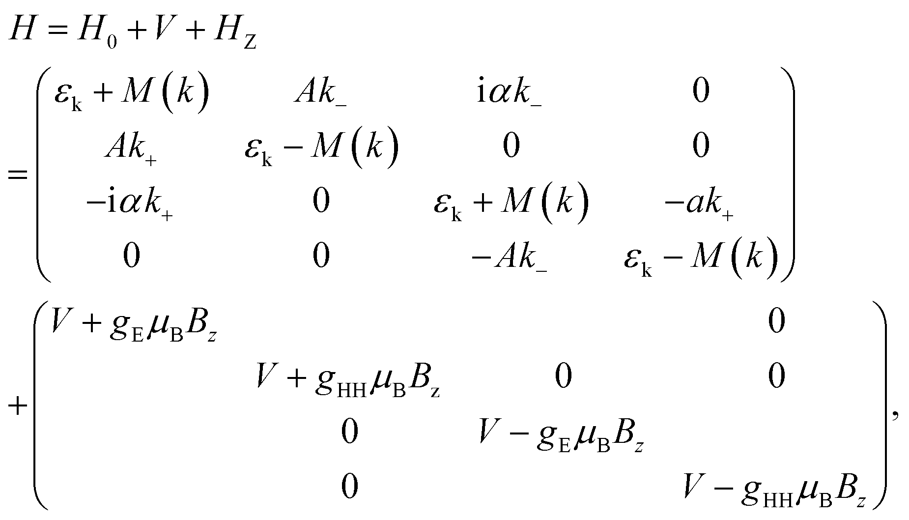 | (1) |
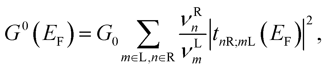
 , εk = C − D(kx2 + πy2), M(k) = M − B(kx2 + πy2), k± = kx ± iπy, α is the RSOI strength, and A, B, C, D, and M are the parameters describing the band structure of the HgTe/CdTe QW. Note that the QSH state and band insulator state are characterized by the sign of the parameter M, which is mainly determined by the thickness of the HgTe/CdTe QW4,5 as well as a perpendicular electric field.6 For negative (positive) M, the QW is in the QSH (bulk insulator) state. For a quasi-one-dimensional (Q1D) QSH bar system, shown in Fig. 1(b), the transport property can be obtained by discretizing the Q1D system into a series of transverse strips along the transport direction with sharply narrowed widths at the TICs controlled by the split-gate modulation. Using scattering matrix theory,16 the transmission amplitudes from the m-th input mode to the n-th output mode tnR;mL are obtained. We can obtain the total conductance of the QSH system at a temperature of zero from the Landauer–Büttiker formula,
 | (2) |
 | (3) |
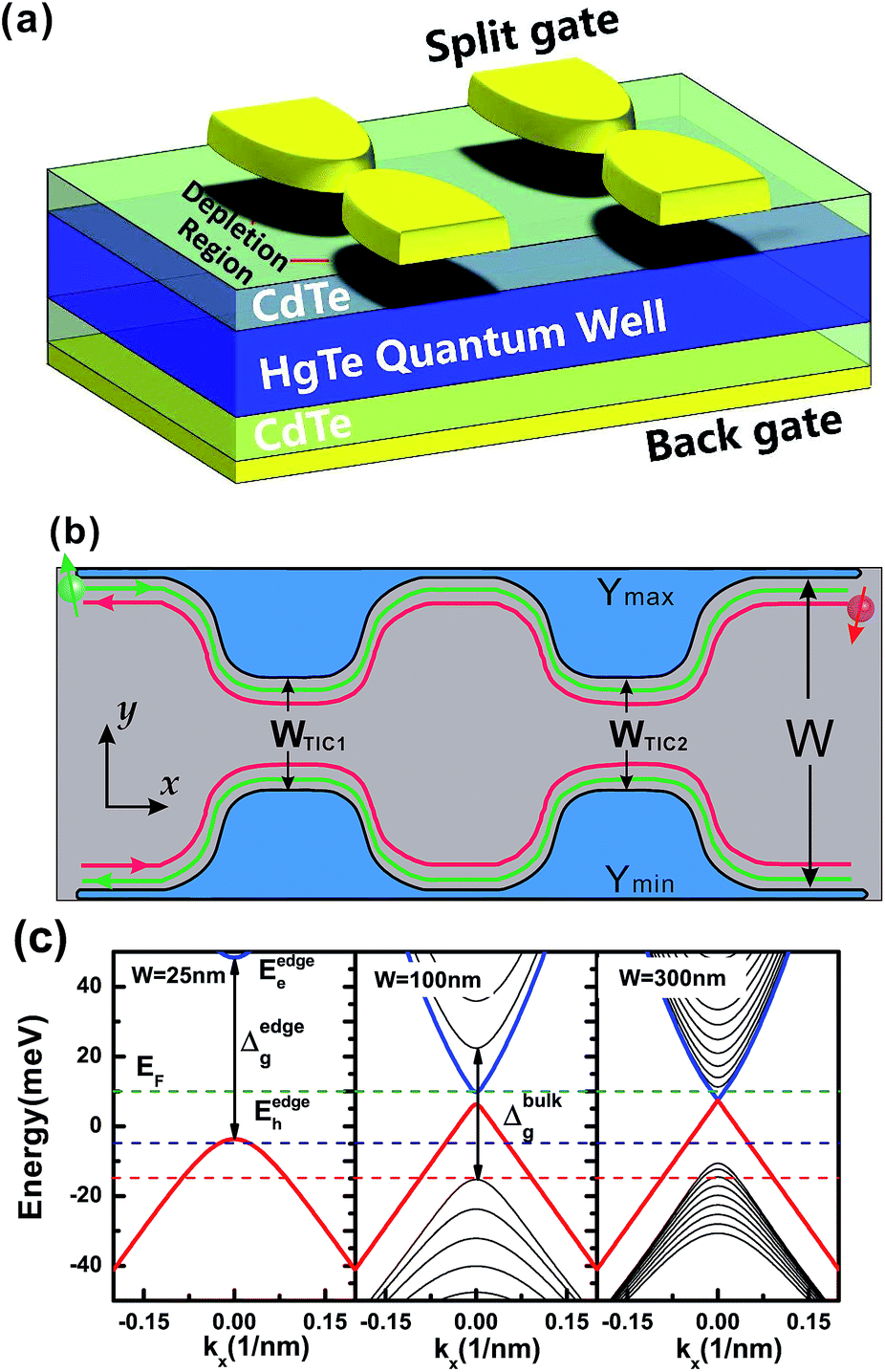 | ||
| Fig. 1 (a) Schematic diagram of the HgTe quantum well based Hall bar structure with dual TICs. The HgTe quantum well is grown in the [001] direction with a channel along the [100] crystallographic direction. (b) Schematic illustration of spin-polarized QSH edge states. WTIC1 (WTIC2) is the width of the first (second) TIC. The green/red lines indicate the trajectories of spin-up/spin-down carriers via the QSH edge states. (c) The energy dispersions of the HgTe QSH system with different QW widths. The thickness of the HgTe well is 7 nm. The dashed lines indicate the positions of the Fermi energies chosen for the calculations in Fig. 2. | ||
3 Results and discussion
In our proposal, the HgTe quantum well is grown in the [001] direction with a channel along the [100] crystallographic direction. The thickness of this HgTe well is 7 nm, guaranteeing the existence of band inversion.4–6 The CdTe barrier is wider than 20 nm, at which value the tunneling through CdTe layers24 can be well suppressed. Finally the QSH states can be realized for both electron and hole branches. We start by investigating the carrier transport properties in this QSH bar system without RSOI or magnetic fields. Fig. 2(a)–(c) show the conductance variations with the dual TIC width modulations in three different ways, i.e. varying the widths of dual TICs simultaneously (a), and fixing the width of one TIC and varying the width of the other one (b and c). Due to the finite size effect,55,56 a finite gap can be opened in the energy spectra (see Fig. 1(c)) and the gap keeps increasing when reducing the width of the TICs as shown in Fig. 2(d). The electrostatic control of the position of the chemical potential with respect to the Dirac point allows for precise modulation of the transport properties. If the Fermi energy locates in this opened energy gap, there is no available propagating mode in the TIC region. Instead, carriers move in evanescent modes that decay rapidly in the TIC region, leading to the suppression of transmission. For extremely narrow TICs, we can always observe vanished conductance, as shown in Fig. 2(a), regardless of the incident Fermi energy we choose, since the gap is very large. For the green curve, i.e. EF = 10 meV, the Fermi energy is close to the Dirac point of the QSH TI state. Even though only a small gap is opened when the widths of the TICs are controlled to just below 100 nm, the Fermi energy has already located in this gap, consistent with the conductance drop observed in our calculations. For the blue curve, i.e. EF = −5 meV, the Fermi energy lies far from the Dirac point of the QSH TI state. Therefore, we need a much larger gap in the TIC region with a further reduced width to block the edge channel. Note that the Fermi energy of the blue curve still does not touch the edge of the bulk subbands (bulk propagating modes) even when the TICs are as wide as the leads. In the above two cases, only the edge state contributes to the transport and thus the conductance saturates to the value of 2G0 as we relax the TICs. Note that when the incident energy is fixed to EF = −15 meV the Fermi level is so far from the Dirac point that it is able to cross several bulk propagating subbands as the widths of the TICs get larger (see Fig. 1(c)). As we expect, the conductance does not saturate with the width of the TICs but exhibits a step-like feature, which corresponds to the opening of new bulk propagating modes in the TIC regions as they become wider. Furthermore we can observe a dip in the conductance curve at around W ≈ 85 nm. The conducting channels come from both the QSH TI edge states and the bulk propagating states; the wave functions of the QSH TI states are squeezed in the central quantum dot region and couple with the bulk states in the narrow TICs. Due to the destructive quantum interference when the charge carriers transmit or reflect at TICs, carriers are localized in the quantum dot without transmission. In Fig. 2(b) and (c) we confirm that each single TIC can effectively block the carrier transport, making our proposed TI quantum dot able to work as an electronic storage device, which we will discuss in more detail later. | ||
| Fig. 2 (a)–(c) The conductance as a function of the width of the TICs for three different Fermi energies EF = 10 meV (green lines), −5 meV (blue lines), and −15 meV (red lines). (a) The widths of dual TICs are changed simultaneously (WTIC1 = WTIC2 = WTIC). (b) The width of the second TIC is fixed (WTIC2 = 50 nm) and the width of the first TIC is changed (WTIC1 = WTIC). (c) The width of the first TIC is fixed (WTIC1 = 50 nm) and the width of the second TIC is changed (WTIC2 = WTIC). The width of the QSH bar is always W = 300 nm. (d) The conduction band (blue line), valence band (red line), and energy gap (green dashed line) in the edge-state spectrum as a function of the width of the TICs. | ||
To confirm the analytical prediction of carrier localization, we plot the density distribution of both topological edge states and bulk states for the three cases in Fig. 3(a)–(c), corresponding to the dips in Fig. 2(a)–(c), respectively. The Fermi energy is EF = −15 meV, and the widths of dual TICs are as follows, (a) WTIC1 = WTIC2 = 85 nm, (b) WTIC1 = 108 nm, WTIC2 = 50 nm, and (c) WTIC1 = 50 nm, WTIC2 = 108 nm. Our calculations demonstrate the localized bound states in the quantum dot. Carriers can be confined in these coupled quantum states with appropriate TIC widths and Fermi energies. Despite the similarity of the charge trapping phenomenon to conventional quantum dots, the physical content is different in our system. In our TI quantum dot, the bound states arise from the coupling between one topological edge state and the bulk states and thus the conductance shows a single dip in Fig. 2(a)–(c). In the case of common quantum confinement of double barriers, the conductance exhibits oscillating behaviors with multiple local minima58 arising from the formation of Fabry–Pérot modes. We can adiabatically change the Fermi energy to approach such conditions of charge trapping. This provides the possibility of storing information in these coupled quantum states. However, there are some difficulties in realizing this application, which are the following. (1) It is difficult to break the edge channel via coupling and (2) the transition from the trapping phase to the transferring phase is rather smooth. (3) There is additional scattering between the bulk states outside of the depletion regions and the unexpected defect/trap states in the depletion regions, which may decrease the trapping efficiency of the carriers and jeopardize the validity of the hard-wall confinement potential assumption, and (4) the new mechanism of bound states in the quantum dot does not give rise to some functional benefits. For the purpose of making an electronic storage element, a very sharp transition is required to boost the device performance, e.g. a quick switch, large on/off ratio, low standby power, etc.
 | ||
| Fig. 3 The density distribution of the carrier in both the edge states and bulk states. The Fermi energy is fixed at EF = −15 meV. The widths of the TICs are as follows: (a) WTIC1 = WTIC2 = 85 nm; (b) WTIC1 = 108 nm, WTIC2 = 50 nm; (c) WTIC1 = 50 nm, WTIC2 = 108 nm. | ||
To find a possible solution, we consider the carrier transport purely in the helical edge channels by tuning the Fermi energy to EF = −5 meV. The bulk subbands are too far from this Fermi energy to contribute to carrier transport. In the absence of RSOI or a magnetic field, we obtain a block diagonal Hamiltonian leading to the time-reversal symmetry for the upper and lower 2 × 2 blocks. Therefore we can calculate the carrier transport of the spin-up or down state separately. Fig. 4 shows the density distribution of the helical edge states in the system for different TIC configurations. For a clear physical picture, we only take the spin-up carriers into consideration. In Fig. 4(a), the TICs are adequately wide with remaining edge channels in the whole QSH bar device region including the central quantum dot and dual TICs. The carriers propagate along the edge channel and perfectly transport through the topological quantum dot. If the second TIC is blocked, as in Fig. 4(b), one can see clearly that the carriers from the left incident lead can transport along the top edge into the quantum dot and be reflected to the opposite edge with the same spin orientation due to the helicity of the topological edge states. Then carriers leak out of the quantum dot easily, also via the edge channels. Since the width of the first TIC is wide enough, the coupling between the top and bottom helical edge states is very weak. Carriers can transport freely in these edge channels that are well kept in the TICs. If we reduce the width of the first TIC as we did for the second TIC, the coupling between the edge states in the opposite edges becomes spectacular, as we can see in Fig. 4(c). The maximum local probability |ψTESσ|2(σ = ↑, ↓) is approximately 0.17 between the dual TICs which is significantly enlarged with respect to the configuration shown in Fig. 4(b), in which the maximum local probability |ψTESσ|2(σ = ↑, ↓) is about 0.09. This gap indicates that the carriers cannot reflect back to the left incident lead freely and tend to be stored in the quantum dot. If we keep reducing the width of the TIC, the coupling is strong enough to break the topological edge modes and the first TIC is blocked as well as the second TIC. One can first apply the pinch-off voltage on the split-gate to block the second TIC, after the charges are injected from left lead via the spin-polarized helical edge channel, and then block the first TIC with the same technique.
 | ||
| Fig. 4 The density distribution of the carrier in the edge states. The Fermi energy is fixed at EF = −5 meV. The widths of TICs are as follows: (a) WTIC1 = WTIC2 = 100 nm; (b) WTIC1 = 100 nm, WTIC2 = 10 nm; (c) WTIC1 = 50 nm, WTIC2 = 10 nm. | ||
In sharp contrast to conventional semiconductor quantum dots, the quantum states in our topological quantum dot are fully spin-polarized helical edge states at an appropriate Fermi energy in the bulk gap (in our discussion, EF = −5 meV). The trapped charges show ring-like density distributions near the boundary as we demonstrated in Fig. 4(c). More importantly, the spin-angular momentum locking, determined by the BHZ Hamiltonian, gives rise to spin-polarized charge currents, i.e. the trapped spin-up carriers rotate clockwise and spin-down carriers rotate counterclockwise without spin flip or spin relaxation.59 If we inject spin polarized currents into the quantum dot, the polarized spin can be stored as well as the charge in the form of persistent spin/charge currents accounting for the topological protected edge states, which are robust against local perturbations. Note that Klinovaja, et al., demonstrated a novel all-electric-controlled spin filter in the same frame of TIC in two dimensional TIs.56 This can be used to generate the desired spin-polarized current. More importantly, this is also compatible with the topological quantum dot charge storage elements proposed in this work and people can dramatically reduce the integration difficulties in making a complete setup. This feature sheds new light on constructing charge/spin trapping memory elements for both electronic and spintronic devices.
To proceed further, we examine the impact of the aforementioned important HgTe QW band parameter M. As we have discussed, M determines the presence of TI edge state or only trivial bulk insulator (BI) state.4 Modulation of the parameter M is achieved mainly by changing the HgTe QW thickness and/or by tuning the bottom gate voltage. The bottom gate is commonly used technology in semiconductor nano-devices, giving us a practical way to switch the system between the TI and BI states. In Fig. 5(a)–(c) we show the QD conductance G as a function of the Fermi energy EF with different values of the band parameter M. The different tunneling process between BI (M > 0) and TI (M < 0) can be observed. In all three cases, the widths of the two TICs are fixed to 100 nm. For the BI system, the conductance vanishes when the incident Fermi energy was located in the gap of the TICs due to the absence of propagating modes. For higher Fermi energies, conductance plateaus appear as well as many oscillations. Each plateau corresponds to the opening of a new bulk subband in the TICs. The oscillations originate from the Fabry–Pérot interference between the transmitted and reflected carriers in the quantum dot. For TI systems, the resonances are observed even when the Fermi energies are located not only in the bulk-subband energy regions but also in the small TI edge gap. When the incident Fermi energies are located in the bulk gap but not in the edge gap of the TICs, the transmission is nearly perfect, accounting for the helical edge channels. The oscillation of the transmission is smeared out since the backscattering process is suppressed, i.e. few Fabry–Pérot modes are formed. The switching between the TI state and BI state leads to a strongly enhanced on/off ratio of this QSH bar device. This observation provides us with an additional way of controlling the carrier transport properties in the proposed HgTe QSH bar device.
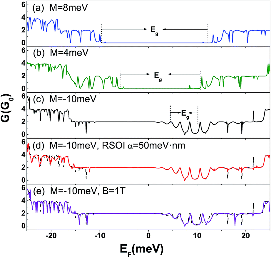 | ||
| Fig. 5 Fermi energy dependence of the QD conductance with fixed TIC widths (WTIC1 = WTIC2 = 100 nm). Panels (a)–(c) show the switch between BI and TI determined by different values of the band parameter M without considering RSOI or magnetic field perturbations. (a) M = 8 meV, (b) M = 4 meV, and (c) M = −10 meV. Panels (d) and (e) are obtained based on almost the same settings as (c) except for including (d) RSOI α = 50 meV nm (red line) or (e) a magnetic field B = 1 T (purple line). The black dashed lines indicate α = 0 and B = 0 in the QD. | ||
So far, we have studied the carrier transport through the proposed QSH bar system exclusively under electric modulations. For completeness, we further investigate the carrier transport through the HgTe QSH bar in the presence of RSOI or a magnetic field in the quantum dot. Fig. 5(d) shows the conductance as a function of the incident Fermi energy in the presence/absence of RSOI. Since the TI edge states are immune to perturbations of RSOI, the conductance curves at different RSOI strengths (α = 0 and α = 50 meV) are almost the same in the energy region −10 meV < EF < 15 meV, where the conducting channels only come from the TI edge states. If the Fermi energy locates out of the bulk band gap, i.e., EF < −10 meV or EF > 15 meV, the bulk modes are opened in the quantum dot. The RSOI would induce a spin splitting of the bulk subbands, resulting in different Fermi wave vectors kσ (σ = ↑, ↓) for spin-up and spin-down carriers. However the spin splitting is quite small, so one can expect that this spin splitting only leads to slightly different behaviors compared to the case without RSOI in the quantum dot, and this is clearly reflected in Fig. 5(d).
Finally, we consider an external magnetic field applied perpendicularly to the HgTe quantum dot. Fig. 5(e) shows the conductance as a function of the incident Fermi energy EF for B = 1 T and B = 0 T. Interestingly, we find that the positions of the resonance conductance peaks are obviously shifted in a finite magnetic field of B = 1 T. This is because the magnetic field breaks the time-reversal symmetry and shifts the Dirac point in the energy spectrum.59 Beyond the energy range with only a TI edge state, the conductance behaviors are completely different when we apply a finite magnetic field (B = 1 T). More oscillations and sharp dips are observed in our calculations. These dips indicate strong backscattering in the quantum dot. This can be understood by the semi-classical picture; the magnetic field can bend the trajectory of the carriers in favor of cyclotron motion. Charge carriers have more chance to meet with each other before transmission through the quantum dot, and this will enhance the interference between different modes in the quantum dot. If the magnetic field is very large, the cyclotron orbit radius is smaller than the size of the quantum dot and the conductance can be fully suppressed. For small RSOI and magnetic fields, as we employed in above simulation, the TI edge states are well preserved. All of the aforementioned features needed to make a spin-polarized charge trapping device element are retained in the proposed quantum dot even in the presence of a small RSOI and/or a magnetic field.
4 Conclusions
In summary, we have theoretically investigated the carrier transport through a topological quantum dot formed using dual TICs in HgTe QWs with inverted band structures. The conductance of the system can be tuned by changing the Fermi energy, the width of the TICs (via tuning the split-gate voltages), and the QW bandgap M (via tuning the bottom gate voltages and/or the thickness of the HgTe QW). Upon changing the incident Fermi energies, the transmission exhibits a series of Fano resonances originating from the Fabry–Pérot modes localized in the quantum dot, or a rather flat plateau arising from the TI edge state. In particular, with appropriate control of the Fermi energy and the TIC configurations, it is possible to trap charge carriers into the spin-polarized helical TI edge states in the quantum dot, which may pave a new path of constructing charge/spin trapping memory elements for both electronic and spintronic devices. Finally we show that the proposed topological quantum dot memory element is immune to small RSOI or magnetic fields, as well as local perturbations.Acknowledgements
This work was supported by the MOST (Grants No. 2015CB921503, 2016YFE0110000 and 2016YFA0202300), the Opening Project of MEDIT, CAS and the Preferred Foundation of Director of IMECAS.References
- C. L. Kane and E. J. Mele, Phys. Rev. Lett., 2005, 95, 146802 CrossRef CAS.
- L. Fu, C. L. Kane and E. J. Mele, Phys. Rev. Lett., 2007, 98, 106803 CrossRef PubMed.
- B. A. Bernevig and S. C. Zhang, Phys. Rev. Lett., 2006, 96, 106802 CrossRef PubMed.
- B. A. Bernevig, T. Hughes and S. C. Zhang, Science, 2006, 314, 1757–1761 CrossRef CAS PubMed.
- M. König, S. Wiedmann, C. Brüne, A. Roth, H. Buhmann, L. W. Molenkamp, X. L. Qi and S. C. Zhang, Science, 2007, 318, 766–770 CrossRef PubMed.
- W. Yang, K. Chang and S. C. Zhang, Phys. Rev. Lett., 2008, 100, 056602 CrossRef PubMed.
- D. Hsieh, D. Qian, L. Wray, Y. Xia, Y. S. Hor, R. J. Cava and M. Z. Hasan, Nature, 2008, 452, 970–974 CrossRef CAS PubMed.
- Y. Xia, D. Qian, D. Hsieh, L. Wray, A. Pal, H. Lin, A. Bansil, D. Grauer, Y. S. Hor, R. J. Cava and M. Z. Hasan, Nat. Phys., 2009, 5, 398–402 CrossRef CAS.
- Y. L. Chen, J. G. Analytis, J. H. Chu, Z. K. Liu, S.-K. Mo, X. L. Qi, H. J. Zhang, D. H. Lu, X. Dai, Z. Fang, S. C. Zhang, I. R. Fisher, Z. Hussain and Z. X. Shen, Science, 2009, 325, 178–181 CrossRef CAS PubMed.
- M. Miao, Q. Yan, C. Van de Walle, W. Lou, L. Li and K. Chang, Phys. Rev. Lett., 2012, 109, 186803 CrossRef CAS PubMed.
- D. Zhang, W. Lou, M. Miao, S. Zhang and K. Chang, Phys. Rev. Lett., 2013, 111, 156402 CrossRef PubMed.
- M. Z. Hasan and C. L. Kane, Rev. Mod. Phys., 2010, 82, 3045 CrossRef CAS.
- X. L. Qi and S. C. Zhang, Rev. Mod. Phys., 2011, 83, 1057 CrossRef CAS.
- D. Hsieh, Y. Xia, D. Qian, L. Wray, J. H. Dil, F. Meier, J. Osterwalder, L. Patthey, J. G. Checkelsky, N. P. Ong, A. V. Fedorov, H. Lin, A. Bansil, D. Grauer, Y. S. Hor, R. J. Cava and M. Z. Hasan, Nature, 2009, 460, 1101 CrossRef CAS PubMed.
- Z. Wu and J. Li, Nanoscale Res. Lett., 2012, 7, 90 CrossRef PubMed.
- L. Z. Lin, F. Cheng, L. B. Zhang, D. Zhang and W. Yang, Phys. Rev. B: Condens. Matter Mater. Phys., 2013, 87, 245311 CrossRef.
- H. Lu, A. Zhao and S. Shen, Phys. Rev. Lett., 2013, 111, 146802 CrossRef PubMed.
- Z. Siu, M. Jalil and S. Tan, Sci. Rep., 2014, 4, 5062 CrossRef CAS PubMed.
- Y. Jing, S. Huang, K. Zhang, J. Wu, Y. Guo, H. Peng, Z. Liu and H. Xu, Nanoscale, 2016, 8, 1879–1885 RSC.
- S. Bauer and C. Bobisch, Nat. Commun., 2016, 7, 11381 CrossRef CAS PubMed.
- A. Rahim, A. Levin, G. Gusev, Z. Kvon, E. Olshanetsky, N. Mikhailov and S. Dvoretsky, 2D Mater., 2015, 2, 044015 CrossRef.
- C. Liu, T. Hughes, X. Qi, K. Wang and S. Zhang, Phys. Rev. Lett., 2008, 100, 236601 CrossRef PubMed.
- L. Du, I. Knez, G. Sullivan and R. Du, Phys. Rev. Lett., 2015, 114, 096802 CrossRef PubMed.
- S. Küfner and F. Bechstedt, Phys. Rev. B: Condens. Matter Mater. Phys., 2014, 89, 195312 CrossRef.
- Q. Liu, X. Zhang, L. Abdalla and A. Zunger, Adv. Funct. Mater., 2016, 26, 3259–3267 CrossRef CAS.
- G. Zhang, X. Li, G. Wu, J. Wang, D. Culcer, E. Kaxirasf and Z. Zhang, Nanoscale, 2014, 6, 3259–3267 RSC.
- L. Kou, B. Yan, F. Hu, S. Wu, T. Wehling, C. Felser, C. Chen and T. Frauenheim, Nano Lett., 2013, 13, 6251–6255 CrossRef CAS PubMed.
- H. Zhang, Y. Ma and Z. Chen, Nanoscale, 2015, 7, 19152–19159 RSC.
- F. Ma, G. Gao, Y. Jiao, Y. Gu, A. Bilic, H. Zhang, Z. Chen and A. Du, Nanoscale, 2016, 8, 4969–4975 RSC.
- M. Yuan, W. Ji, M. Ren, Y. Wang and H. Zhao, RSC Adv., 2016, 6, 86089–86094 RSC.
- X. Li, S. Zhang and Q. Wang, Nanoscale, 2017, 9, 562–569 RSC.
- Q. Liu, X. Zhang, L. Abdalla, A. Fazzio and A. Zunger, Nano Lett., 2015, 15, 1222–1228 CrossRef CAS PubMed.
- J. Zhou, Q. Sun, Q. Wang, Y. Kawazoed and P. Jena, Nanoscale, 2016, 8, 11202–11209 RSC.
- S. Küfner, J. Furthmüller, L. Matthes, M. Fitzner and F. Bechstedt, Phys. Rev. B: Condens. Matter Mater. Phys., 2013, 87, 235307 CrossRef.
- Y. Ma, Y. Dai, C. Niu and B. Huang, J. Mater. Chem., 2012, 22, 12587–12591 RSC.
- A. Wang, X. Zhang and M. Zhao, Nanoscale, 2014, 6, 11157–11162 RSC.
- H. Zhao, C. Zhang, W. Ji, R. Zhang, S. Li, S. Yan, B. Zhang, P. Li and P. Wang, Sci. Rep., 2016, 6, 20152 CrossRef CAS PubMed.
- H. Zhao, W. Ji, C. Zhang, P. Li, S. Zhang, F. Li, P. Wang, S. Li and S. Yan, J. Mater. Chem. C, 2017, 5, 2656–2661 RSC.
- D. N. Sheng, Z. Y. Weng, L. Sheng and F. D. M. Haldane, Phys. Rev. Lett., 2006, 97, 036808 CrossRef CAS PubMed.
- C. Xu and J. E. Moore, Phys. Rev. B: Condens. Matter Mater. Phys., 2006, 73, 045322 CrossRef.
- C. J. Wu, B. A. Bernevig and S. C. Zhang, Phys. Rev. Lett., 2006, 96, 106401 CrossRef PubMed.
- L. Fu and C. L. Kane, Phys. Rev. B: Condens. Matter Mater. Phys., 2007, 76, 045302 CrossRef.
- B. J. van Wees, H. vanHouten, C. W. J. Beenakker, J. G. Williamson, L. P. Kouwenhoven, D. van der Marel and C. T. Foxon, Phys. Rev. Lett., 1988, 60, 848 CrossRef CAS PubMed.
- D. A. Wharam, T. J. Thornton, R. Newbury, M. Pepper, H. Ahmed, J. E. F. Frost, D. G. Hasko, D. C. Peacock, D. A. Ritchie and G. A. C. Jones, J. Phys. C: Solid State Phys., 1988, 21, L209 CrossRef.
- D. Loss and D. P. DiVincenzo, Phys. Rev. A, 1988, 57, 120 CrossRef.
- A. Imamoglu, D. D. Awschalom, G. Burkard, D. P. DiVincenzo, D. Loss, M. Sherwin and A. Small, Phys. Rev. Lett., 1999, 83, 4204 CrossRef CAS.
- R. Hanson, L. P. Kouwenhoven, J. R. Petta, S. Tarucha and L. M. K. Vandersypen, Rev. Mod. Phys., 2007, 79, 1217 CrossRef CAS.
- M. A. Kastner, Rev. Mod. Phys., 1992, 64, 849 CrossRef.
- A. Galindo and M. A. M. Delgado, Rev. Mod. Phys., 2002, 74, 347 CrossRef.
- B. Zhou, H. Lu, R. Chu, S. Shen and Q. Niu, Phys. Rev. Lett., 2008, 101, 246807 CrossRef.
- J. C. Y. Teo and C. L. Kane, Phys. Rev. B: Condens. Matter Mater. Phys., 2009, 79, 235321 CrossRef.
- A. Ström and H. Johannesson, Phys. Rev. Lett., 2009, 102, 096806 CrossRef PubMed.
- V. Krueckl and K. Richter, Phys. Rev. Lett., 2011, 107, 086803 CrossRef.
- C. W. Huang, S. T. Carr, D. Gutman, E. Shimshoni and A. D. Mirlin, Phys. Rev. B: Condens. Matter Mater. Phys., 2013, 88, 125134 CrossRef.
- L. B. Zhang, F. Cheng, F. Zhai and K. Chang, Phys. Rev. B: Condens. Matter Mater. Phys., 2011, 83, 081402(R) CrossRef.
- J. Klinovaja and D. Loss, Phys. Rev. B: Condens. Matter Mater. Phys., 2015, 92, 121410(R) CrossRef.
- J. P. Bird, Electron Transport in Quantum Dots, Springer Science+Business Media, New York, 2003 Search PubMed.
- Z. H. Wu, F. M. Peeters and K. Chang, Phys. Rev. B: Condens. Matter Mater. Phys., 2010, 82, 115211 CrossRef.
- K. Chang and W. K. Lou, Phys. Rev. Lett., 2016, 106, 206802 CrossRef PubMed.
Footnote |
| † These authors contributed equally to this work. |
| This journal is © The Royal Society of Chemistry 2017 |