
 Open Access Article
 This Open Access Article is licensed under a Creative Commons Attribution-Non Commercial 3.0 Unported Licence
Nonvolatile memory devices based on undoped and Hf- and NaF-doped ZnO thin film transistors with Ag nanowires inserted between ZnO and gate insulator interface
Manoj Kumar,
Hakyung Jeong and
Dongjin Lee *
*
Department of Mechanical Engineering, Konkuk University, 120 Neungdong-ro, Gwangjin-gu, Seoul 05029, Republic of Korea. E-mail: djlee@konkuk.ac.kr
First published on 24th May 2017
Abstract
Nonvolatile memory devices based on solution-processed thin film transistors (TFTs) of sol–gel-derived undoped ZnO and ZnO doped with Hf and NaF incorporating Ag nanowires (AgNWs) as charge trapping media between the ZnO and insulator interface are demonstrated. The transfer characteristics of the devices exhibited a large clockwise hysteresis due to the carrier trapping at the AgNWs between the ZnO and dielectric interface. The memory devices showed a remarkable, wide, programmable memory window during program/erase operations, which is attributed to the charge carrier trapping and de-trapping in the ZnO/AgNW/SiO2 structure. The device based on Hf-doped ZnO exhibited a larger memory window compared to the device based on NaF-doped ZnO. The threshold voltage shifts of these devices measured over various durations exhibited a large memory window. The fabricated transistor memory devices showed long term retention time characteristics, indicating excellent electrical reliability and stability.
Introduction
Recently, metal oxide semiconductors have been intensively investigated for application as an active layer in thin film transistors (TFTs). Among them, the wide band gap semiconductor, zinc oxide (ZnO), has been paid a lot of attention due to its superior electrical performance and good optical transmittance compared to the conventional a-Si:H and organic materials.1 Undoped and doped zinc oxide are widely investigated as channel materials in the TFTs due to their high field mobility, good uniformity, and low processing temperatures. Most of the research is focused on enhancing the performance of the key parameters of the TFTs, however, their application has been rapidly extended to a variety of other areas such as system-on-panel (SOP), memory-in-pixel, and transparent memory displays.2–4 Various materials such as ferroelectric materials, nano-floating gate dielectrics, and polymer electrets have been proposed to generate memory effect in TFT devices.5–7 Among them, the nano-floating gate dielectric process is considered promising for high performance memory devices. In these device structures a floating gate is used to store and release charge with the memory state represented by a shift in the threshold voltage. Various charge trapping media such as noble metals, viz., Ag, Au, and Pt8–10 and dielectrics, viz., Si3N4, Al2O3, Sm2O3, and SmTiO3 are explored.11,12 Such nanocomponents of these memory transistors play an important role in enhancing the device performance in terms of hysteresis window and retention time. Recently, Liu et al. utilized directional silver nanowire (AgNW) to improve TFT performance.13 However, randomly distributed low density and high-density AgNWs would be beneficial as charge trapping media in memory devices. Charge trapping and de-trapping at the semiconductor layer is strongly influenced by the electronic bands of the trapping level. It is highly desirable to adopt solution-based approaches to fabricate the entire memory device so that the electronic devices could eventually be cost effective and environment-friendly. Solution-processed metallic AgNWs are selected as charge trapping media for their more efficient charge trapping as well as better compatibility with the solution processes. Moreover, AgNWs can induce electric fields and the system is mechanically stable as well as reversible. In this paper, we fabricate and demonstrate the performances of solution-processed memory devices based on undoped and Hf- and NaF-doped ZnO TFTs with a layer of AgNWs as the charge trapping media at the interface between the semiconducting channel and gate insulator. The memory devices are shown to have a remarkable, wide, programmable memory window during program/erase operations.Experimental details
The reagents, copper(II) chloride (CuCl2, 99.99%), poly(vinylpyrrolidone) (PVP, 99%), silver nitrate (AgNO3, 100%), ethylene glycol (99.99%), zinc acetylacetonate hydrate (99.995%) and ZnO powder were purchased from Sigma-Aldrich.For the synthesis of AgNWs, 100 mL of ethylene glycol in a glass flask was heated at 155 °C for 1 h under continuous mechanical stirring. Reagent solutions of 40 mM CuCl2, 294 mM PVP, and 94 mM of AgNO3, were prepared in ethylene glycol. A preheated solution of CuCl2 was added and the resulting solution was heated for 15 min. Finally, 30 mL of PVP solution and 30 mL of AgNO3 solution, respectively, were injected into the flask. The color of the reaction mixture changed from yellow to light gray and then to gray within 1 h, indicating the formation of AgNWs. After this, the reaction flask was cooled to room temperature. The product was washed with acetone and stored in methanol under ambient conditions.
Three separate precursor solutions were prepared. For the first undoped ZnO precursor, zinc acetylacetonate hydrate was dissolved in 2-methoxyethanol to a concentration of 0.1 M. Second precursor for Hf doped ZnO was prepared by dissolving zinc acetylacetonate hydrate in 2-methoxyethanol to a concentration of 0.1 M and then, hafnium chloride (2 at%) was added and stirred for 2 h to ensure complete dissolution.
The third precursor was prepared by dissolving ZnO powder in ammonium hydroxide to a concentration of 0.1 M. The precursors were kept in a refrigerator for 1 day to increase the solubility of ZnO. Then, 20 mL of deionized (DI) water and NaF (the concentration was varied from 5–15 at%) were added to the ZnO solution.
For the device fabrication, a B-doped, p-type Si wafer (resistivity in the range of 0.001–0.003 Ω cm) served as the gate electrode, and 300 nm thermally grown SiO2 was used as the dielectric layer. Prior to spin coating, SiO2/Si substrates were cleaned ultrasonically, first in acetone, and subsequently in methanol, for 10 min each. They were further rinsed with DI water for 5 min. The prepared AgNW suspension was spin coated at 2000 rpm for 20 s on the SiO2/Si substrate. Three different sets of samples were prepared using three undoped and doped with Hf and NaF ZnO precursors. The solutions of undoped ZnO and ZnO doped with Hf and NaF were spin coated at 4000 rpm for 40 s to obtain 25 nm thick ZnO thin films. The films were first dried on a hot plate at 200 °C for 10 min to dispose off residual solvents. This process was repeated twice to obtain the desired thickness of the films. Finally, the films were annealed at 400 °C for 1 h in a tube furnace to enable the decomposition and oxidation of the precursors. Finally, Al electrodes were thermally grown on the active layers using a shadow mask, with the channel width and length maintained at 1000 and 100 μm, respectively. The thickness of the resulting source and drain electrodes was ∼100 nm. A schematic of the fabricated nonvolatile memory device based on the undoped and doped ZnO TFTs with AgNWs sandwiched between the semiconductor and gate dielectric layers is presented in Fig. 1(a). Current–voltage (I–V) measurements were performed on a semiconductor analyzer (Keithley 4200) equipped with a probe station.
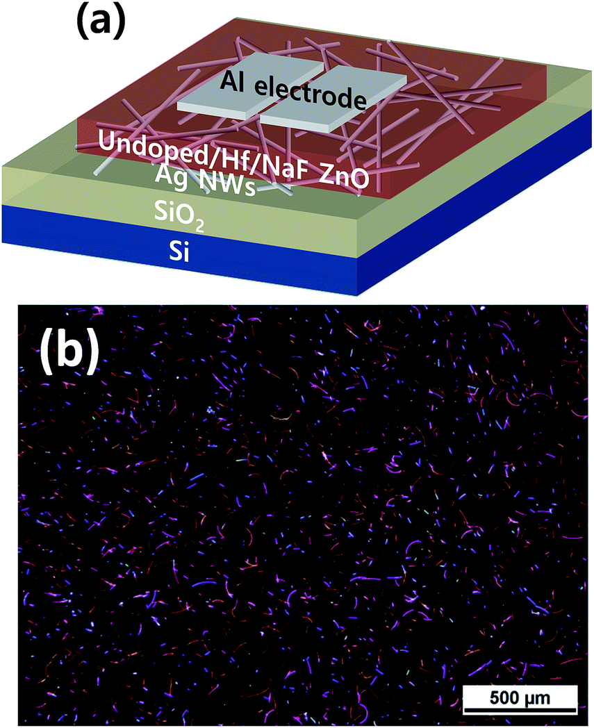 | ||
| Fig. 1 (a) Schematic of the fabricated nonvolatile memory devices based on undoped ZnO and Hf- and NaF-doped ZnO TFTs with AgNWs embedded between the semiconductor and gate dielectric layers, (b) optical microscopy image of AgNWs coated on SiO2/Si. | ||
Results and discussion
An optical microscopy image of the AgNWs coated on the SiO2/Si substrate is shown in Fig. 1(b). A randomly distributed network of AgNWs with an average length of the AgNWs of ∼15 μm is observed. A medium density of AgNWs is achieved to form the nonvolatile TFT memory device.Fig. 2 shows XRD patterns of undoped and doped with Hf and NaF doped ZnO thin films. Undoped and NaF doped ZnO thin films XRD patterns exhibited (100), (002) and (101) diffraction peaks. The peak intensity of the (002) plane is stronger than that of (100) and (101) plane in the NaF doped ZnO thin films. The peak intensity of (002) diffraction peak is significantly increased and other peaks suppressed with the increase of NaF doping concentration from 5 to 10 at% and further increase of NaF doping concentration to 15 at%, (100) and (101) diffraction peaks marginally increased. The absence of diffraction peaks related to Na metals or any of its oxides and F oxides, suggests the Na and F incorporation into the ZnO matrix as substitution or interstitial position. NaF doping does not affect the position of the diffraction peaks, but it effectively changes the intensity corresponding to (100), (002) and (101) diffraction peaks. On the other hand, Hf doped ZnO XRD pattern revealed only dominant (002) diffraction peak, indicating highly prepared c-axis orientation perpendicular to the substrate. Also, no metallic Hf or its oxide related peaks are observed in the diffraction pattern, which imply that Hf is effectively doped into the ZnO. It is found that the (002) diffraction intensity of Hf doped ZnO thin film is much higher than that of undoped and NaF doped ZnO thin films, demonstrating better crystalline structure.
 | ||
| Fig. 2 XRD spectra of 2 at% Hf-doped ZnO and 5–15 at% NaF-doped ZnO. | ||
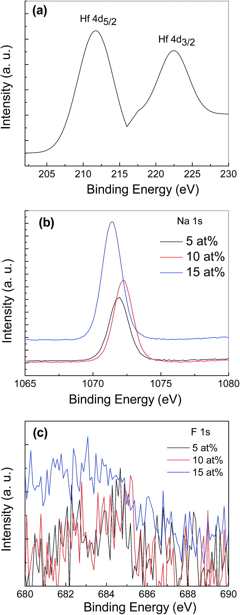
The distribution of Hf, Na and F elements in the ZnO thin films doped with 2 at% Hf and NaF with different concentration ranging from 5 to 15 at% was examined through determining the chemical bonding states by XPS and is shown in Fig. 3. The Hf doped film showed clear Hf spectra at binding energies of 211.18 and 222.32 eV, respectively [Fig. 3(a)]. The peak at 211.18 eV is assigned to Hf 4d5/2 and the peak located at 222.32 eV is associated to Hf 4d3/2 and coincided well with reported values of Hf 4d5/2 and Hf 4d3/2.14 The XPS results clearly showed Na spectra at the binding energy of 1071.40–1072.23 eV, which coincides well with the reported value, to reveal the presence of Na in the ZnO thin films [Fig. 3(b)]. That is the peak position of the binding energy of Na+ oxide, which indicates that the NaF-doped ZnO thin films were doped with Na+.15 The peak corresponding to F 1s orbital in the ZnO is shown in Fig. 3(c). The obtained weak F 1s signal can be assigned to the formation of Zn–F bonds formed in the ZnO lattice. The elements dopant concentration in the ZnO thin films are listed in Table 1. It is evident from the XPS analysis that the concentration of Hf and NaF in the deposited films is slightly less than the initial dopant addition in the starting solution. The observed elements in the doped ZnO suggested that doping process is performed successfully.
 | ||
| Fig. 3 XPS spectrum of (a) 2 at% Hf-doped ZnO, (b) Na 1s and (c) F 1s in 5–15 at% NaF-doped ZnO. | ||
| Elements | NaF (5 at%) | NaF (10 at%) | NaF (15 at%) | Hf (2 at%) |
|---|---|---|---|---|
| Na | 4.83 | 9.51 | 13.62 | — |
| F | 0.27 | 0.33 | 0.37 | — |
| Hf | — | — | 1.66 |
The output characteristics of the TFTs based on undoped ZnO, and ZnO doped with 2 at% Hf and NaF (5–15 at%) with embedded AgNWs is shown in Fig. 4(a)–(e). The gate-source voltage, VGS was varied from 0 to 60 V in 10 V increments. All the TFTs clearly demonstrated a typical n-type field-effect transistor behavior with an n-type active semiconductor channel layer. As the device turned on, the output characteristics of all the TFTs revealed a clear pinch off and current saturation in the electrical response. The output current of undoped and Hf doped ZnO begins to decrease with the increase of VDS. The decrease of IDS with the increase of VDS in the undoped ZnO and Hf doped ZnO may be due to self-heating effect during operation as the devices cannot effectively dissipate the heat evolved in the channel. As a result, more free carriers and grain boundaries are created in the channel layer. These defects can form traps prolong the resistance and enhance the temperature along the channel path to generate further defects which in turn decreases the charge density. Self-heating effect did not notice in the NaF doped ZnO TFT devices. Therefore, IDS of undoped and Hf doped ZnO is obtained less than that of NaF doped ZnO. These TFTs were operated according to the standard field-effect transistor theory. The saturation field-effect mobility can be determined from the linear fit of the (IDs)1/2 vs. VGS plot in the saturation regime.16
| IDS = (μsat CiW/2L)(VGS − VTH)2 | (1) |
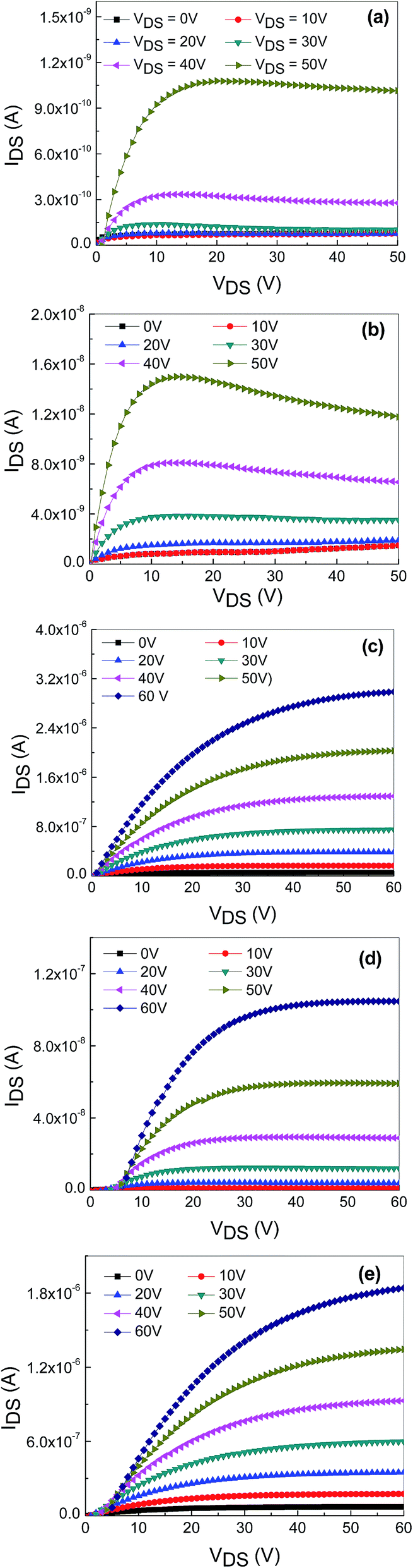 | ||
| Fig. 4 Output characteristics (IDS vs. VDS) of the nonvolatile memory devices based on undoped ZnO, Hf-doped ZnO and 5–15 at% NaF-doped ZnO with embedded AgNWs (a–e). | ||
To identify the feasibility of the AgNWs-embedded memory devices based on undoped ZnO and Hf-doped ZnO, dual sweep transfer characteristics (IDS vs. VGS) were measured at a VDS of 10 V, as shown in Fig. 5(a). A significant hysteresis is observed between the forward and reverse gate voltage sweeping in both the devices. Being n-type devices, both the undoped and Hf-doped ZnO TFTs showed a clear clockwise hysteresis. The hysteresis window for the AgNWs-embedded devices based on undoped and Hf-doped ZnO is over 20 and 80 V, respectively. This hysteresis window is relatively large compared to that of the conventional metal-oxide-semiconductor field-effect transistor (MOSFET) memory device with NPs inserted between the gate insulators.17 The observed hysteresis of transfer characteristics is a clear indication that the charge carriers are trapped at the AgNWs layer. The wide hysteresis window in the memory device based on Hf-doped ZnO TFT with AgNWs could be due to Hf occupancy at either the interstitial or substitutional position of the Zn sites in the ZnO matrix. As a result, extra charge carriers are generated, a large number of which are trapped at the AgNWs layer during the forward and reverse sweep voltage. Fig. 3(b) shows the transfer characteristics (IDS vs. VGS) of AgNWs-embedded TFTs based on 5–15 at% NaF-doped ZnO annealed at 400 °C. A clear clockwise hysteresis window is observed in all the devices, with the window widening with increasing NaF doping. The hysteresis window for these devices widened from ∼25 to ∼40 V with the increase in the NaF doping from 5 to 15 at%. This is attributed to the electron/hole trapping in the AgNWs during the positive and negative voltage sweeping. When a positive bias is applied, charge carriers accumulate in the channel close to the semiconductor and dielectric interface and get trapped in the AgNWs during the forward and reverse voltage sweeps. The widened hysteresis window is due to increased charge carrier injection and trapping from the channel layer to AgNWs. On the other hand, all the TFTs without the AgNWs between the semiconducting layer and the dielectric layers exhibited negligible hysteresis, indicating that there is no memory effect (Fig. 5(c)).
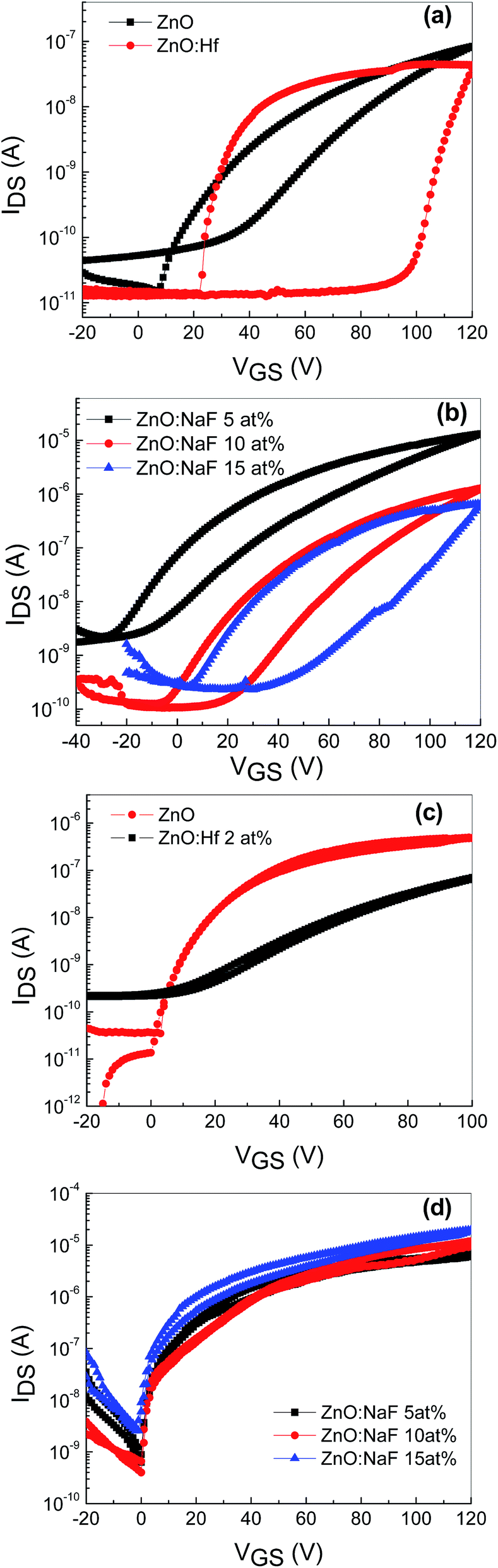 | ||
| Fig. 5 Transfer characteristics (IDS vs. VGS) of the TFT memory devices based on (a) undoped and Hf-doped ZnO with AgNWs (b) 5–15 at% NaF-doped ZnO with AgNWs, (c) undoped and Hf-doped ZnO TFTs without AgNWs, and (d) NaF-doped ZnO TFTs without AgNWs. | ||
Furthermore, to confirm the viability of utilizing undoped and Hf- and NaF-doped TFTs as charge trapping nonvolatile memory devices, the transfer characteristics (IDS vs. VGS) were measured after a program and erase operation. A gate voltage of +50 V and −50 V were applied for the writing and erasing process, respectively, for TFTs based on both undoped and Hf-doped ZnO with embedded AgNWs. In both memory devices, under the positive bias condition (writing process), a clear transfer curve shift occurred over 40 V from the initial stage, and it reverted back to the initial state upon applying a gate voltage of −50 V (erasing process), as shown in Fig. 6(a) and 4(b). In case of memory devices based on NaF-doped ZnO TFTs with AgNWs, when a gate voltage of +50 V was applied, transfer curve shifted over 7 to 13 V with varied NaF concentration (5 to 15 at%) and it returned to its initial state when the gate voltage of −50 V was applied, as depicted in Fig. 6(c)–(e). The change in the threshold voltage associated with the trapped charge carriers per AgNW is relatively large compared to the conventional TFT memory device with embedded nanoparticles (NP) in the gate insulators.18
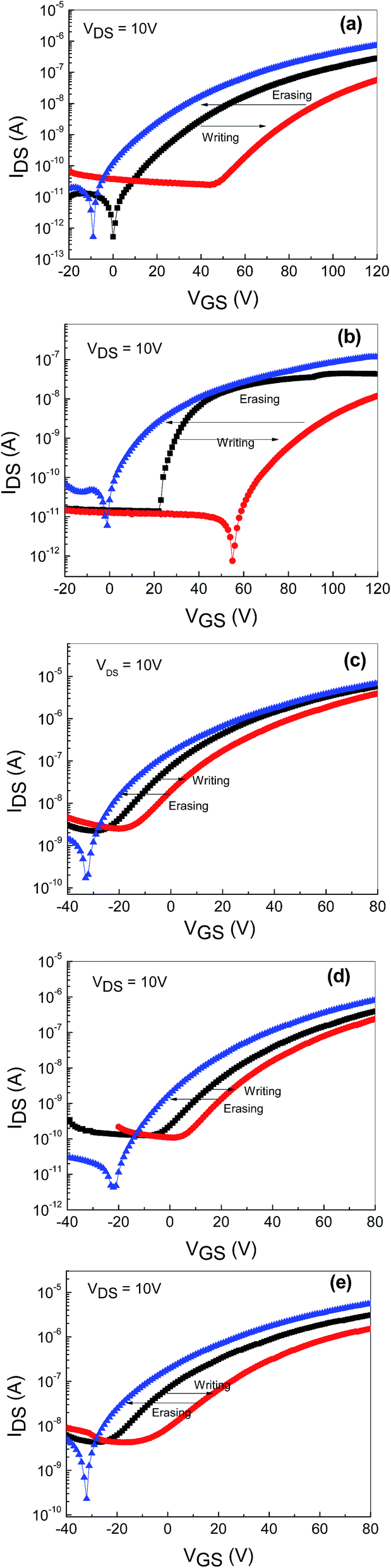 | ||
| Fig. 6 Transfer characteristics (IDS vs. VGS) of the nonvolatile memory device with AgNWs based on (a) undoped and Hf-doped ZnO and (b) ZnO TFTs with 5–15 at% NaF (c–e), according to different writing (VGS = 50 V)/erasing (VGS = −50 V) at the drain bias, VDS = 10 V. | ||
Fig. 7 shows the threshold voltage shifts (ΔVTH) of the memory devices with embedded AgNWs based on undoped- and HF-doped ZnO [Fig. 7(a)] and NaF-doped ZnO [Fig. 7(b)] as a function of the programming time. ΔVTH is measured with respect to the initial un-programmed value and the programmed gate voltage (VGS) with the amplitude of +50 V and consequently, erasing characteristics was measured by observing ΔVTH as a function of the programming time with the amplitude of −50 V. ΔVTH increases with the increasing programming time. A positive gate voltage induces an expected positive ΔVTH shift because a portion of the induced charge carriers responsible for the shift of ΔVTH are captured at the AgNWs layer. The captured charge carriers act like interface-fixed charge carriers, resulting in ΔVTH shift toward the positive VGS direction. The gate voltage-dependent erasing characteristics were investigating by applying a negative gate bias. The ΔVTH swas now shifted toward a negative gate bias, because some or all of the precaptured charge carriers are de-trapped. The threshold voltage decreases with the erasing time. As seen in the figure, at the shortest programming/erasing time of 10−5 s, the nonvolatile memory devices exhibited larger threshold voltage shifts, which are enough to be sensed.
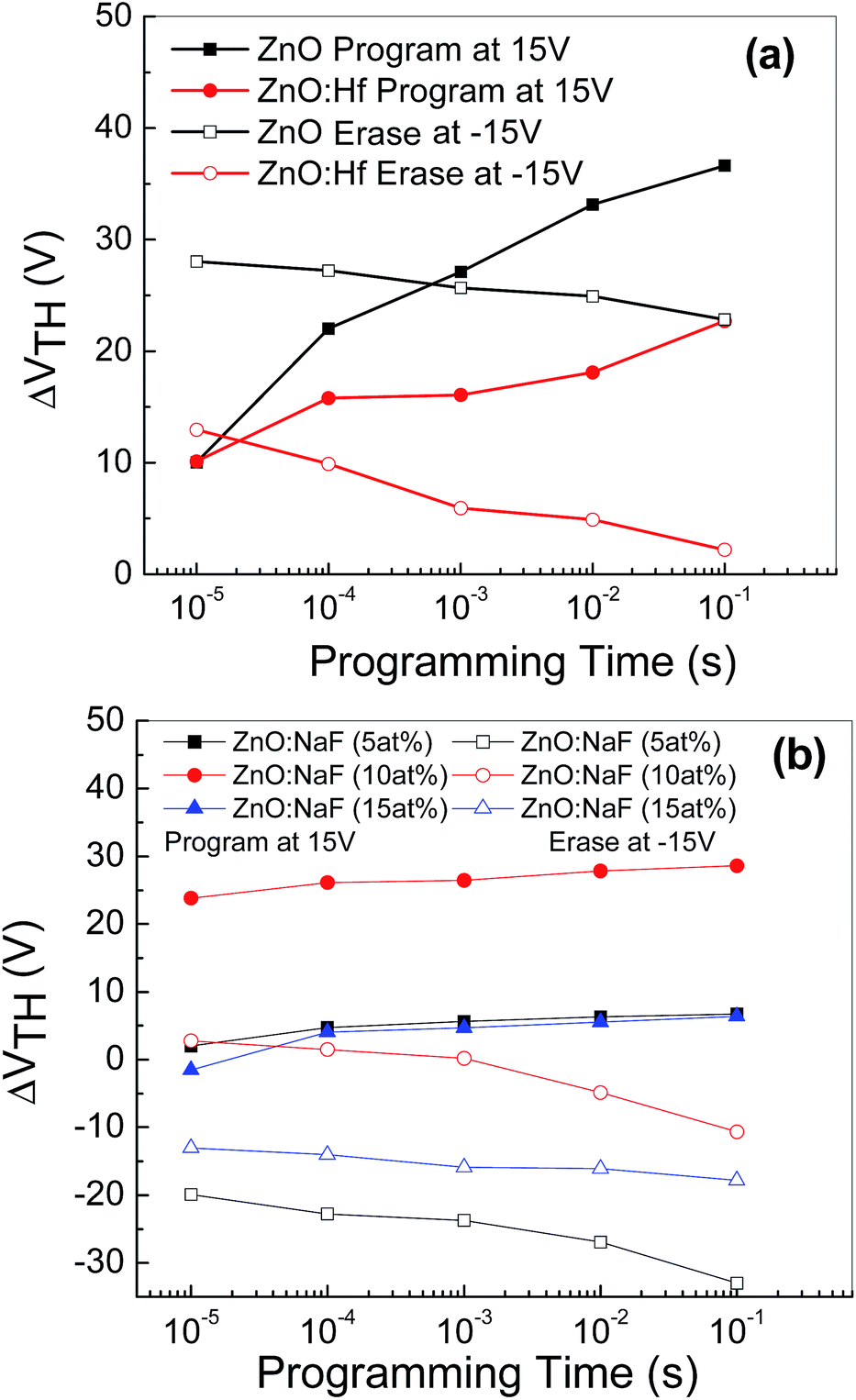 | ||
| Fig. 7 Programming/erasing characteristics of the memory device with AgNWs based on (a) undoped and Hf-doped ZnO, (b) 5–15 at% NaF-doped ZnO, exhibiting threshold voltage shifts. | ||
The data retention time characteristics of the memory devices with embedded AgNWs based on the undoped and Hf-doped ZnO is shown in Fig. 8(a) and that of the NaF doped ZnO device is depicted in Fig. 8(b). After the writing and erasing at VGS = ±50 V, the drain current (IDS) was measured at VGS = 0 V and VDS = −15 V. The ON state current is slightly reduced, initially, in case of the undoped ZnO TFT memory device, whereas in the Hf-doped ZnO memory device the ON state current remained nearly constant. However, the OFF state current remained nearly constant at 10−11 A up to 103 s. Thus, these AgNWs memory devices exhibited more than three orders of ON/OFF (ION/IOFF) ratio for 103 s. However, the memory devices based on NaF-doped ZnO revealed that the ON state current of the device with 5 at% NaF initially increased and then saturated; further, for the device with 10 and 15 at% NaF-doping, ON state current reduced by almost one order of magnitude, possibly due to the release of the shallowly trapped charge carriers at the interface between NaF-doped ZnO and AgNWs. Nevertheless, the observed OFF state current was almost constant at 10−11 A up to 103 s. Thus, after 103 s, the memory devices with embedded AgNWs still retain more than four orders of magnitude ON/OFF ratio (ION/IOFF). The slight variation in the ION/IOFF ratio indicates that AgNWs creates a discrete charge carrier storage center.19
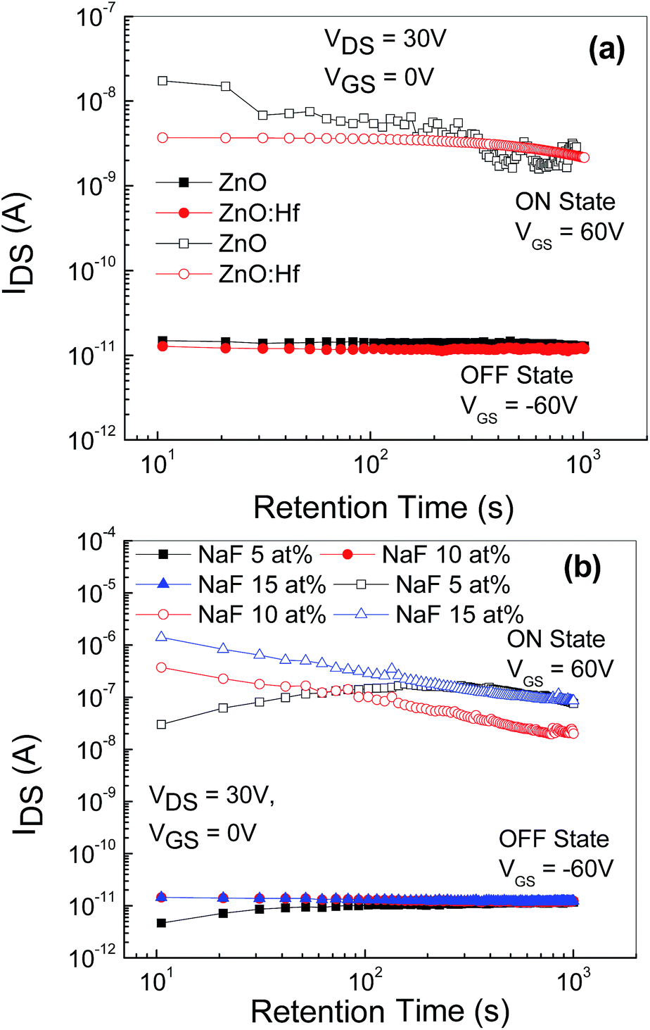 | ||
| Fig. 8 Charge retention characteristics of programmed and erased IDS as a function of time for memory devices with AgNWs based on (a) undoped and Hf doped ZnO TFTs, (b) NaF-doped ZnO with the NaF concentration ranging from 5 to 15 at%. | ||
Fig. 9 shows the energy band diagram of the (a) 2 at% Hf- and (b) 5 at% NaF-doped ZnO memory devices. In the Hf-doped ZnO memory device embedded with AgNWs, the charge carrier trapping occurs over a larger window in comparison to that in the NaF-doped ZnO memory device. There is a drastic difference in the band gap between Hf and NaF doped ZnO. The valence band offset from the Fermi level obtained by an extrapolation method in the valence band X-ray photoelectron spectra suggested that the relative difference between the Fermi level and the conduction band minimum (CBM) increased by 1.3 eV for NaF-doped ZnO. This strongly correlates with the decrease in the carrier concentration. The NaF concentration in the ZnO matrix may cause the Na substitution sites to surpass the interstitial sites and become dominant; as a result, Na will neutralize the charge carriers in the ZnO thin films, thereby reducing the number of charge carriers. In consequence, the charge carrier concentration induced at the AgNWs/SiO2 interface by the applied gate electric field is lowered. On the other hand, the difference between the Fermi level and CBM of Hf-doped ZnO is comparatively lower than that of NaF-doped ZnO, resulting in the increase of charge carriers. Presumably, a large number of charge carriers travel toward AgNWs/SiO2 and get trapped in the AgNWs layer. During the electrical programming, the charge carriers from the Hf-doped ZnO channel can be easily trapped in the AgNWs, which results in the larger memory window. Optical transmittance of the doped ZnO is measured to investigate band gap of the films. Optical transmittance of doped ZnO with 2 at% Hf and NaF with different concentrations from 5 to 15 at% is shown in Fig. 10. It is observed that optical band gap of NaF doped ZnO slightly decreases at first when doping concentration increase from 5 to 10 at% and then increases with the increase of NaF concentration to 15 at%. However, there is a large difference in the band gap of Hf and NaF doped ZnO thin films. NaF doped ZnO thin films band gap is higher than that of Hf doped ZnO thin film. The change of optical band gap is interpreted by Moss–Burstein shift, where the change is the result of a large increase in the free carrier concentration and corresponding downward shift of the Fermi level. The optical bang gap of 2 at% Hf- and 5 at% NaF-doped in ZnO estimated using the Tauc's plot ((αhν)2 vs. hν) from the transmittance measurements is shown in Fig. 11.
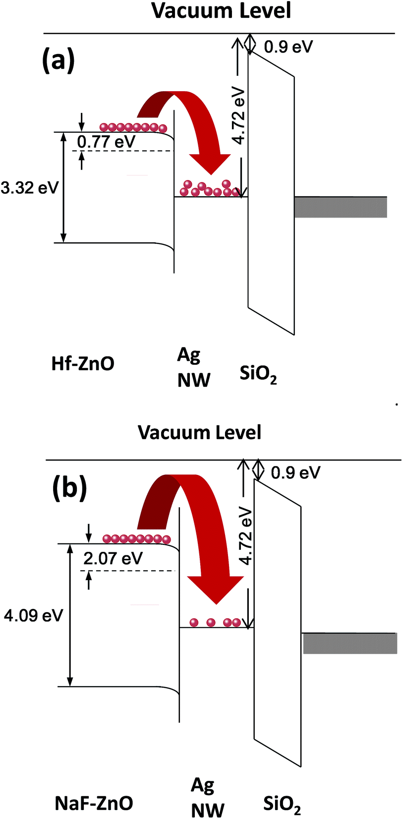 | ||
| Fig. 9 Energy band diagram of (a) Hf-doped and (b) NaF-doped ZnO TFTs with embedded AgNWs. | ||
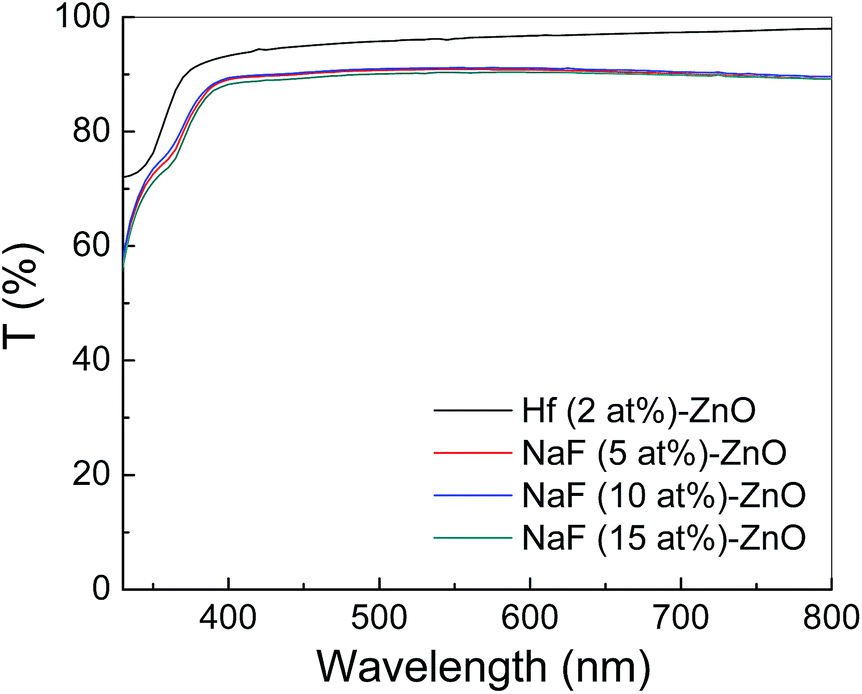 | ||
| Fig. 10 Optical transmittance spectra of ZnO thin films doped with 2 at% Hf and NaF with different concentrations ranging from 5 to 15 at%. | ||
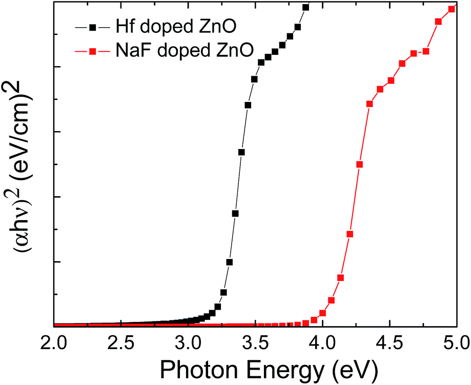 | ||
| Fig. 11 (αhν)2 versus photon energy (E) plot of Hf- and NaF-doped ZnO thin films. | ||
Conclusion
Solution-processed sol–gel derived undoped and doped ZnO TFT nonvolatile memory are demonstrated with embedded AgNWs at the insulator layer as charge storage media. Hf doped ZnO TFT memory exhibited very wide gate bias dependent hysteresis window in comparison to undoped and NaF doped ZnO. The transfer characteristics (IDS–VGS) of all the memory devices can be right shifted by applying a positive gate voltage and brought back effectively by applying a negative gate voltage, suggesting charge trapping and de-trapping in AgNWs. All the memory devices showed more than three orders of magnitude ON/OFF ratio for 103 s. These low-cost AgNWs-embedded ZnO TFT memory devices prepared by the inexpensive solution-based process utilized here can be potential candidates for new, emerging systems such as the memory panel displays and transparent electronic devices.Acknowledgements
This research was supported by the Basic Science Research Program through the National Research Foundation of Korea (NRF) funded by the Ministry of Science, ICT, and Future Planning (2015R1C1A1A02037326). This work was also supported by a 2017 KU Brain Pool Fellowship of Konkuk University.Notes and references
- J. Chang, Z. Lin, M. Lin, C. Zhu, J. Zhang and J. Wu, J. Mater. Chem. C, 2015, 3, 1787–1793 RSC.
- S. Chen, W. P. Zhang, X. M. Cui, S. J. Ding, Q. Q. Sun and W. Zhang, Appl. Phys. Lett., 2014, 104, 103504 CrossRef.
- S. H. Lee, J. Kim, S. H. Yoon, K. A. Kim, S. M. Yoon, C. Byun, C. S. Hwang, G. H. Kim, K. I. Cho and S. W. Lee, IEEE Electron Device Lett., 2015, 36, 585–587 CrossRef CAS.
- C. H. Park, S. Im, J. Yun, G. H. Lee, B. H. Lee and M. M. Sung, Appl. Phys. Lett., 2009, 95, 223506 CrossRef.
- R. C. G. Naber, C. Tanase, P. W. M. Blom, G. H. Gelinck, A. W. Marsman, F. J. Touwslager, S. Setayesh and D. M. de Leeuw, Nat. Mater., 2005, 4, 243–248 CrossRef CAS.
- M. J. Ahn and W. J. Cho, Appl. Phys. Lett., 2016, 109, 252106 CrossRef.
- Y. H. Chou, S. Takasugi, R. Goseki, T. Ishizone and W. C. Chen, Polym. Chem., 2014, 5, 1063–1071 RSC.
- D. Gupta, M. Anand, S. W. Ryu, Y. K. Choi and S. Yoo, Appl. Phys. Lett., 2008, 93, 224106 CrossRef.
- L. Zhen, W. Guan, L. Shang, M. Liu and G. Liu, J. Phys. D: Appl. Phys., 2008, 41, 135111 CrossRef.
- A. Suresh, S. Novak, P. Wellenius, V. Misra and J. F. Muth, Appl. Phys. Lett., 2009, 94, 123501 CrossRef.
- J. S. Jung, S. H. Rha, U. K. Kim, Y. J. Chung, Y. S. Jung, J. H. Choi and C. S. Hwang, Appl. Phys. Lett., 2012, 100, 183503 CrossRef.
- J. L. Her, F. H. Chen, C. H. Chen and T. M. Pan, RSC Adv., 2015, 5, 8566–8570 RSC.
- H. C. Liu, Y. C. Lai, C. C. Lai, B. S. Wu, H. W. Zan, P. Yu, Y. L. Chueh and C. C. Tsai, ACS Appl. Mater. Interfaces, 2015, 7, 232–240 CAS.
- C. H. Ahn, J. H. Kim and H. K. Cho, J. Electrochem. Soc., 2012, 159, H384–H387 CrossRef CAS.
- S. Ilican, J. Alloys Compd., 2013, 553, 225–232 CrossRef CAS.
- T. S. Kang, J. H. Koo, T. Y. Kim and J. P. Hong, Appl. Phys. Express, 2013, 6, 011101 CrossRef.
- J. T. Li, L. C. Liu, P. H. Ke, J. S. Chen and J. S. Jeng, J. Phys. D: Appl. Phys., 2016, 49, 115104 CrossRef.
- Q. Hu, S. C. Lee, Y. J. Baek, H. H. Lee, C. J. Kang, H. M. Kim, K. B. Kim and T. S. Yoon, J. Nanopart. Res., 2013, 15, 1435 CrossRef.
- T. C. Chang, F. Y. Jian, S. C. Chen and Y. T. Tsai, Mater. Today, 2011, 14, 608–615 CrossRef CAS.
| This journal is © The Royal Society of Chemistry 2017 |