DOI:
10.1039/C7RA03369A
(Paper)
RSC Adv., 2017,
7, 32383-32390
Novel III-Te–graphene van der Waals heterojunctions for optoelectronic devices
Received
22nd March 2017
, Accepted 29th May 2017
First published on 26th June 2017
Abstract
Gallium telluride presents interesting properties for applications in optoelectronic devices, such as solar panels and radiation detectors. These applications, however, have been hindered due to the low mobility of charge carriers and short lifetime of photoexcitations in this material. In this work we propose that these limitations could be overcome by van der Waals heterostructures of recently exfoliated GaTe monolayers and graphene sheets, combining the high photoabsorption of the former with the ballistic transport of the latter. Our analysis indicates that such structures have a binding energy greater than that of graphene bilayers and that the band offset is such that transfer of photoexcited electrons from GaTe to graphene should be spontaneous. To investigate the consequences of the relative position of graphene's Dirac cone with the band edges of the photon absorber, we propose two hypothetical new materials with the same atomic arrangement as GaTe: InTe and TlTe. Thermodynamic and dynamical analyses indicate that monolayers of these crystals, which should also present high photoresponsivity, are stable. Specifically for the case of TlTe we found that the band edges should coincide with graphene's Dirac cone in the brillouin zone, resulting in optimal transfer of photoexcited carriers.
1 Introduction
Most optoelectronic devices, such as sensors and photovoltaic panels, depend on materials that not only interact strongly with photons but also that sustain the photoexcited carriers long enough to form an electrical signal at the contacts. For semiconductors, therefore, in addition to a direct band gap no greater than the energy of the incoming radiation, high mobility free carriers and long lived photoexcitations are also needed. Mobility depends on the effective mass of the carriers at the band edges, which is an intrinsic property of the material, but generally the limiting factor is scattering by lattice vibrations or defects. The lifetime of photoexcited carriers is mostly limited by trap states introduced by charged defects in the material. Direct band gaps are also needed to preclude the intermediation of phonons in band-to-band photoexcitations. Specifically for photovoltaics, a band gap between 1.5 and 2.5 eV is necessary, since about 95% of the Sun's radiation is in this range.
Possessing a direct band gap of 1.7 eV,1–3 gallium telluride presents an intense excitonic absorption.4–6 In addition to solar cells and thermoelectric devices,7–10 GaTe has also been considered for detection of γ and X-ray radiation.11–13 This because with a high average atomic number and a crystal structure of relatively dense packing, GaTe has a high stopping power for very energetic photons. Moreover, its moderate band gap is optimal for radiation detection. Small band gaps imply dark-current, or thermal noise, to the radiation measurement. Larger band gaps, on the other hand, increase the so called Fano noise, which is linked to the reduction of the carrier statistics.14 Both these effects reduce the accuracy of the spectral deconvolution, preventing for instance specific determination of the isotope source of the radiation.
These applications of GaTe, however, have been hampered by very low carrier mobilities as well as significant trap centers.9,11,13,15–19 Surface treatments,12 stoichiometric shifts and co-doping13 have been suggested as approaches to minimize these limitations. However, these methods alone are not expected to produce a significant breakthrough that could make GaTe an economically viable candidate for application in photovoltaics or radiation detection.
Recent techniques to exfoliate layered materials have turned focus back into gallium telluride, which has also been successfully synthesized through chemical vapor deposition (CVD) on a mica substrate.20 In a recent work, researchers have measured the photoresponse of multilayer GaTe flakes, finding that not only its photosensitivity is highest among all reported for layered material based photodetectors, but also its photoresponse (6 ms) is extremely fast.1 The measured mobility of 0.2 cm2 V−1 s−1 is still extremely low.
Graphene, on the other hand, is a material which conducts electrons ballistically even at room temperature, with mobilities up to 106 cm2 V−1 s−1 reported for suspended samples.21–23 The absence of an intrinsic band gap has prevented its application replacing traditional semiconductors. For example, graphene's photoresponsivity is six orders of magnitude smaller than that reported for GaTe multilayered flakes.1 In the specific case of radiation detection, graphene is completely unfit, because it does not possess neither high atomic packing nor a dense electrosphere. Important experimental developments in recent years, however, have made the synthesis of heterostructures composed by the stacking of 2D materials a reality.24–28 These structures could be used to combine the properties of graphene with other materials, circumventing the limitations of the isolated components.29
In this work we propose a 2D heterostructure composed of a graphene sheet stacked on GaTe layers (GaTe–Gr) which should present promising characteristics for applications in solar panels and possibly also in radiation detection devices. We also study theoretically stable layers of InTe and TlTe with the same crystal structure of GaTe. The integration of these materials with graphene could also boost massive fabrication of commercially viable structures. Recently, large area perovskite-graphene hybrid solar panels have been produced with promising results.30 In these panels graphene served as a matrix to connect the perovskite flakes which are otherwise hard to grow as films of large areas. Although there are reports of experimental isolation of GaTe monolayers, the difficulty in the production of films of large extension could be realistically overcome by depositing these flakes on graphene.
2 Methods and computational details
All calculations were performed within the Density Functional Theory approach31 implemented in the Vienna Ab initio Simulation Package (VASP).32,33 The interaction between valence electrons and ions was performed through the full-relativistic Projected Augmented Wave method,34 and for the selection of the plain waves an energy cutoff of 425 eV was chosen to describe the atomic orbitals. For exchange and correlation the Generalized Gradient Approximation in the Perdew–Burke–Ernzerhof35 implementation was used. The sampling of the first brillouin zone for the 2D structures was performed using a 10 × 2 × 1 grid centered at the Γ point. In the cases with graphene, a 15 × 5 × 1 grid was used to localize the Fermi energy with higher accuracy. The band structures were aligned with respect to the vacuum level, obtained via the electrostatic potentials of the systems. In the simulation of 2D materials, enough vacuum was added in the perpendicular direction to avoid spurious interaction between periodic images. When obtaining the best configurations all the atoms where relaxed until the individual forces were smaller than 0.01 eV Å−1. Van der Waals interactions were simulated by the DF-vdW method, proposed by Dion et al.,36 in the optB86b-vdW version.37 Phonon spectra were obtained by using DFT perturbation theory as implemented in the Phonopy code.38
3 Results and discussion
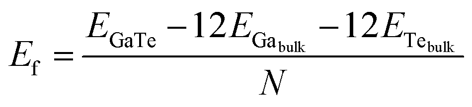
We started simulating one monolayer of GaTe extracted from the most stable monoclinic phase. Our relaxed unit cell consists on 24 atoms (12 Ga atoms and 12 Te atoms) with periodic boundary conditions in the xy plane, as depicted in Fig. 1a. The first brillouin zone is shown in Fig. 1b with the high symmetry points marked on it. The monolayer is also a semiconductor, with a direct band gap at the Γ point (Fig. 1c). The inclusion of spin–orbit coupling (SOC) in the calculation does not change significantly the results. As PBE functionals are known to underestimate the band gaps, it is common to follow two approaches to estimate the error in the calculations: to compare to experimental results (when available) and to calculate the band gap using a more accurate approach, as using hybrid functionals. In the case of GaTe bulk, we calculated the band gap with PBE, obtaining a value of 0.96 eV without SOC and 0.99 eV with SOC, which differ from the experimental one by ∼0.7 eV. We have also calculated the band gap using HSE06 hybrid functionals,39 obtaining a value of 1.61 eV, in great agreement with experiments. On the other hand, we calculated the band gap of GaTe monolayer using HSE06 obtaining a value of 2.16 eV (0.71 eV higher that the PBE result). From all these comparisons, we expect the monolayer to have a band gap corresponding in energy to visible light radiation. To get an insight into the absorption of GaTe, we have plotted the imaginary part of the dielectric constant against energy for the monolayer, as shown in Fig. 1d. As can be observed, the system is expected to have a large part of its absorption in the visible zone of the spectrum. The formation energy of the monolayer, calculated as| |
 | (1) |
was estimated to be −0.371 eV by atom. In this equation, EGaTe is the total energy of the system, EGabulk and ETebulk are the energies of single atoms in the most stable bulk phase and N is the total number of atoms. This result corroborates the thermodynamic stability of the monolayer. However, a dynamic stability criterium should be considered as well. In order to do that, the phonon spectrum was obtained through the entire brillouin zone, resulting in only-positive frequencies (see Fig. 1e).
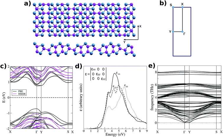 |
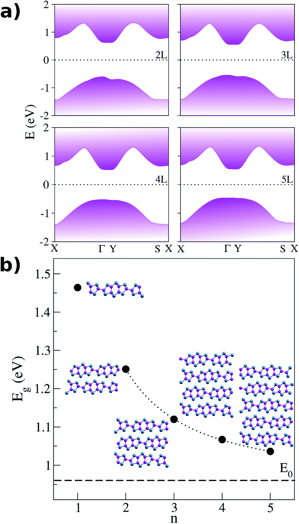
| | Fig. 1 GaTe monolayer properties. (a) Atomic structure; (up) top view of a 4 × 2 supercell, (bottom) side view; pink: Ga, blue: Te; (b) first brillouin zone showing the high symmetry points; (c) electronic band structure obtained with PBE (black) and HSE06 (magenta) functionals (d) three components of the imaginary part of the dielectric constant (e) phonon spectrum | |
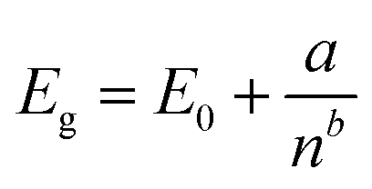
As thicker materials could be needed to maximize absorption of radiation in realistic devices, GaTe multilayers were also simulated. We found that the direct band gap is conserved at the Γ point up to 5 layers, although decreasing with the thickness of the system, as expected due to reduction of the quantum confinement. The conservation of the direct character of the band gap is an important fact, because it implies high absorption efficiency independently of the thickness of the material, contrary to what happens in some transition metal dichalcogenides, which exhibit a thickness-induced direct-to-indirect transition.40,41 Moreover, as the system grow the dispersion between the high symmetry points Γ and Y becomes flatter, being the energy band gap (Eg) of the same size at both points for 5 layers of GaTe. The band structures are shown in Fig. 2a. As Eg should tend to the bulk value as the thickness goes to infinity, we used the following equation to predict the band gap of a system with n layers:42
| |
 | (2) |
where
E0 is the energy band gap for the bulk and
a and
b are constants. The relation presented in
eqn (2) is followed by GaTe systems with 2 to 5 layers. The monolayer does not quite fit in this trend, probably due to the lack of interlayer coupling, as previously reported.
42 We obtained
a = 0.80 eV and
b = 1.46. The calculated energy band gaps and the fitting using
eqn (2) are shown in
Fig. 2b. The electron affinity can be approximated as
where
Vvac is the Hartree potential at infinity and CBM is the conduction band minimum. On the other hand, the ionization potential has been obtained as
where VBM is the valence band maximum. Values are listed on
Table 1. The EA increases monotonically as the number of GaTe layers increases, while the IP fluctuates around a constant value. The estimated EA is in agreement with previously reported values for bulk GaTe.
43 Moreover, both EA and IP are in the order of values reported for similar semiconductors.
44,45 For example, GaSe has an EA of 3.10 eV and an IP of 5.12 eV. Finally, the interlayer energy per atom for
n layers can be calculated as
| |
 | (5) |
where
EGaTen is the energy of the GaTe multilayer,
EGaTe is the energy of the monolayer and
N is the number of atoms in the system. The obtained values, summarized in
Table 1 are in the order of reported energies for other van der Waals structures,
46–48 as bilayer graphene, for example, which has a binding energy of 27 meV at
−1.
 |
| | Fig. 2 GaTe multilayer. (a) Electronic band structures (b) energy band gap as a function of the material width; the dotted line is the fitting done according to eqn (2) and the dashed line marks the energy gap of the bulk; insets: atomic structures; colors according to Fig. 1a. | |
Table 1 Structural and electronic properties of GaTe mono- and multilayers. Values show interlayer energy per atom, electron affinity, ionization potential and energy band gap
| Layers |
Eint (eV at−1) |
EA (eV) |
IP (eV) |
Eg (eV) |
| 1 |
— |
3.63 |
5.09 |
1.46 |
| 2 |
−0.037 |
3.96 |
5.21 |
1.25 |
| 3 |
−0.049 |
4.03 |
5.15 |
1.12 |
| 4 |
−0.056 |
4.07 |
5.13 |
1.07 |
| 5 |
−0.059 |
4.08 |
5.12 |
1.04 |
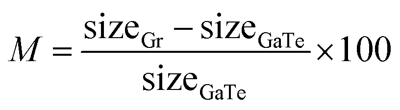
For electronic applications, the known relatively low carrier mobility of GaTe results in a competition between lateral transport and electron–hole recombination. As a strategy to solve this, we propose that the photogenerated carriers in GaTe could be transferred to graphene, as it has been shown for other systems to improve transport by direct vertical charge transfer.25 The 2D heterostructure consists on a monolayer of GaTe and a graphene layer on top of it. Due to the different sizes of the unit cells, there exists a mismatch between the surfaces, which can be estimated as
| |
 | (6) |
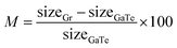
where size
Gr is the dimension of the graphene film and size
GaTe is the size of the GaTe substrate. This mismatch is of 3% in both
x and
y directions accommodating 2 × 10 graphene units by unit cell of GaTe. During the relaxation of the heterostructure all the atoms are allowed to move, and the volume of the whole system is kept constant to the value of the GaTe isolated monolayer. In
Fig. 3 an schematic picture of the final structure is shown. As can be observed, graphene is curved following the shape of the substrate. The interlayer distance, calculated as the difference in height between the highest Te atom and the C atom immediately above it, is in the order of typical van der Waals bonds (3.64 Å). To test the possibility that graphene is waved only because of constrain due to the mismatch between the structures, we relaxed the graphene layer isolated inside the same simulation box, finding that it remains plane. We conclude that graphene acquires this waved form due to the interactions with the GaTe monolayer. The magnitude of the undulation, calculated as the difference in height between the highest and lowest C atoms in the graphene sheet, is of 1.06 Å. The energy gained after stacking both materials is calculated as
| | |
Estack = EGaTe–Gr − EGaTe − EGr
| (7) |
in the equation,
EGaTe–Gr is the energy of the heterostructure,
EGaTe is the energy of an isolated GaTe monolayer and
EGr is the energy of the graphene sheet at infinite distance (as no substrate is present, the sheet remains plane). The obtained value is −0.053 eV per carbon atom, which means that the generation of this 2D material is thermodynamically favourable. The heterostructure is kept together through a combination of van der Waals and ionic interactions. Since no covalent bonds are present at the interface, the conservation of the main electronic properties of each component is expected. If we consider the 2D material as an in-plane current device, there will be a small band offset (see
Fig. 4a) as moving from the region of the GaTe monolayer to the region of graphene. An electron excited in the GaTe monolayer would be promoted to the unoccupied levels corresponding to the graphene cone, which would be quickly dissipated through the sheet towards the metallic contacts upon the application of a bias field. For the suggested application of these heterostructures in radiation detection, a question that arises is related to the noise that is introduced by thermally excited carriers. Germanium based radiation detectors, for example, function with extreme accuracy, but require intense cooling to reduce the concentration of intrinsic carriers which is about 10
13 cm
−3.
49 This is about three orders of magnitude higher than the carrier concentration in graphene at room temperature.
50 In addition to that, the stopping power of germanium (
Z = 32) to high energy radiation is significantly smaller than that of tellurium (
Z = 52). Therefore, the concentration of photoexcited electrons should be significantly high in the GaTe–Gr heterostructure to endure higher levels of thermal noise than Ge radiation detectors. Thus, even if cooling is required, it should not be at the same level as the cryogenic temperatures under which Ge γ detectors function. For solar cells based on GaTe–Gr heterostructures, on the other hand, thermal noise does not represent a limitation.
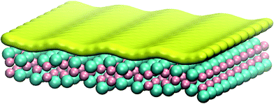 |
| | Fig. 3 Schematic picture of the GaTe–Gr structure; pink: Ga, blue: Te, yellow: C. | |
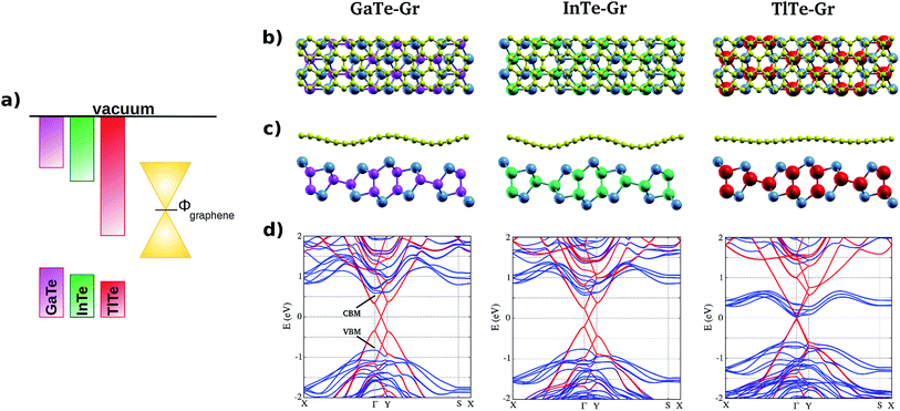 |
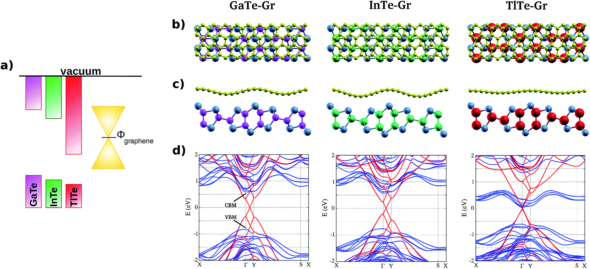
| | Fig. 4 III-Te and III-Te–Gr heterostructures properties. (a) Band alignment of III-Te isolated monolayers with respect to vacuum; graphene work function, calculated to be 4.25 eV, is shown as a reference. (b) Top view of a 2 × 1 supercell of the III-Te–Gr heterostructures. (c) Side view; pink: Ga, green: In, red: Tl, blue: Te, yellow: C. (d) Projected electronic band structures for III-Te–Gr; red: graphene contribution; blue: substrate contribution; VBM and CBM of the substrate are labelled for GaTe–Gr. | |
The projected band structure is depicted in Fig. 4d. The Dirac cone of graphene appears at a k momentum between the high symmetry points Γ and Y. It is known that strain and curvature can displace the cone in the k-space for a graphene sheet,51,52 so the strain due to mismatch and the waving could be the main reasons of the observed displacement. The offset of the band edges in the brillouin zone with the Dirac cone would require the involvement of phonons to mediate the transfer of electrons across the heterostructure, and this could limit the performance of the optoelectronic device, be it a solar cell or a radiation detector. The work function can be calculated as
where
EF is the Fermi energy. For this heterostructure, the obtained
Φ was 4.39 eV. Graphene has also been adsorbed on multilayer GaTe. After structural relaxation, the waving presented by graphene is essentially the same, independently of the number of GaTe layers.
Since the favorable electronic properties of GaTe, specially its moderate direct band gap, stem for its peculiar crystal structure, we propose InTe and TlTe monolayers with the same atomic arrangement as GaTe. These materials, which are also formed by elements with dense electrospheres, exist in different configurations and here we are proposing two hypothetical 2D systems. Nevertheless they have similar atomic arrangements, they should interact with graphene slightly differently from GaTe monolayers and this could result, for instance, in different alignment of the band edges with graphene's Dirac cone. After relaxing the structures and unit cells, we determined the thermodynamic and dynamic stability of the two proposed monolayers. The formation energies resulted to be negative (Table 2), and the phonon spectra did not present negative frequencies. The calculated band gaps, direct and always at the Γ point, decrease when the atomic number of the cation increases. As in the case of GaTe, the inclusion of SOC in the calculations do not change the results significantly. The band alignments, as well as the work function for graphene, as a reference, are depicted in Fig. 4a. Both the electron affinity and the ionization potential increase with the cation atomic number. The size of the unit cells, EF, EA, and IP for the III-Te materials studied are summarized in Table 2.
Table 2 Structural, physical and electronic properties of III-Te monolayers. InTe and TlTe are hypothetical 2D materials with the same atomic configuration as GaTe. Values show the lattice parameters, formation energy per atom, electron affinity and ionization potential
| Material |
(a–b) lattice parameters (Å) |
EF (eV at−1) |
EA (eV) |
IP (eV) |
| GaTe |
4.14–23.97 |
−0.371 |
3.63 |
5.09 |
| InTe |
4.38–25.88 |
−0.340 |
3.83 |
5.22 |
| TlTe |
4.54–26.63 |
−0.061 |
4.63 |
5.30 |
We generated 2D heterostructures coupling these monolayers to graphene, as we have done for GaTe. Due to the different lattice parameters of the materials, different quantities of graphene units can be accommodated on top of them. For InTe and TlTe, 2 × 11 graphene units represent the lowest mismatch, whereas for GaTe 2 × 10 were needed. In Fig. 4c and d the final structures are shown. Again, the graphene sheet is waved following the substrate. The magnitude of the undulations is of 1.45 Å on InTe and 0.49 on TlTe. The energies of stacking (see Table 3) are negative, so the formation of these heterostructures is also thermodynamically favorable. The band structures have similar characteristics for GaTe and InTe. For the case of TlTe, the Dirac cone is centered at the Γ point, which means that in TlTe–Gr heterostructures the charge transfer between the components would be more effective than in GaTe–Gr and InTe–Gr, because the absorption or emission of phonons is not required. On the other hand, the CBM corresponding to the TlTe levels are degenerated with the center of the cone, indicating that the charge transfer after excitation may be not spontaneous, and electron–hole recombination would be competing with the dissipation of the carrier. However, this could be remediated by the application of an electric field to tune the band offset. In a recent work, researchers have been able to shift the Fermi level in graphene mono- and bilayers using a h-BN tunneling barrier.53
Table 3 Structural, physical and electronic properties of III-Te–Gr heterostructures. Values show the mismatch between the substrate and the graphene sheet, the energy of stacking, the interlayer distances and the workfunctions
| Material |
(a–b) M (%) |
Estack (eV per C at) |
dInt (Å) |
Φ (eV) |
| GaTe–Gr |
3.0–3.0 |
−0.053 |
3.64 |
4.39 |
| InTe–Gr |
−0.2–5.0 |
−0.067 |
3.65 |
4.56 |
| TlTe–Gr |
−6.0–2.0 |
−0.039 |
3.40 |
4.70 |
4 Conclusions
We have studied the structural and electronic properties of GaTe mono- and multilayers, which have been recently obtained experimentally by exfoliation of the monoclinic bulk phase. We have shown that these are stable materials, with direct band gaps that decrease as the number of layers increases. Aiming at applications in solar cells and radiation detectors, we have shown that it is theoretically possible to combine GaTe, with its intense response to visible light as well as high energy radiation, with graphene, with its unparalleled carrier transport properties. Photo excited electrons are expected to migrate spontaneously from GaTe into graphene. The concentration of thermally excited carriers in graphene is three orders of magnitude smaller than that of germanium based detectors. Moreover, the higher photoresponse of GaTe should enable a radiation detector based on GaTe–Gr heterostructure to endure greater levels of thermal noise than Ge detectors. Therefore this should not be a major limiting factor in radiation detectors based on these heterojunctions. Solar cells based on our proposed GaTe–Gr heterostructure do not suffer from limitations due to thermal noise. The offset of the band edges of GaTe in the brillouin zone with the Dirac cone in graphene would need the involvement of phonons to mediate the transfer across the van der Waals heterostructure. This limitation should also be compensated by the intense photoresponse of GaTe, with the production of high concentrations of photoexcited electrons. We have also proposed two new materials: InTe and TlTe monolayers with the same atomic arrangement as GaTe, which resulted to be thermodynamic and dynamically stable. These materials present direct and moderate band gaps, and should also possess strong photoresponsivity. The combination of these materials with graphene showed strong binding. In the case of TlTe, the band edges coincided with the Dirac cone in the brillouin zone. The band offset, however, appears to be too small for spontaneous transfer of photoexcited electrons to graphene. This could be circumvented by the application of a small bias field between the two materials.
Acknowledgements
This work was financed by Fundaҫão de Amparo à Pesquisa do estado de São Paulo (FAPESP), Conselho Nacional de Desenvolvimento Científico e Tecnológico (CNPq) and Coordenaҫão de Aperfeiҫoamento de Pessoal de Nível Superior (CAPES). J. A. O.-A. thanks FAPESP for a fellowship (process no. 2016/12021-0).
References
- F. Liu, H. Shimotani, H. Shang, T. Kanagasekaran, V. Zólyomi and N. Drummond, et al., High-Sensitivity Photodetectors Based on Multilayer GaTe Flakes, ACS Nano, 2014, 8(1), 752–760 CrossRef CAS PubMed.
- J. J. Fonseca, S. Tongay, M. Topsakal, A. R. Chew, A. J. Lin and C. Ko, et al., Bandgap Restructuring of the Layered Semiconductor Gallium Telluride in Air, Adv. Mater., 2016, 28(30), 6465–6470 CrossRef CAS PubMed.
- U. S. Shenoy, U. Gupta, D. S. Narang, D. J. Late, U. V. Waghmare and C. N. R. Rao, Electronic structure and properties of layered gallium telluride, Chem. Phys. Lett., 2016, 651, 148–154 CrossRef CAS.
- J. F. Sanchez-Royo, J. Pellicer-Porres, A. Segura, V. Munoz-Sanjose, G. Tobias and P. Ordejon, et al., Angle-resolved photoemission study and first-principles calculation of the electronic structure of GaTe, Phys. Rev. B: Condens. Matter Mater. Phys., 2002, 65(11), 115201 CrossRef.
- J. F. Sánchez-Royo, A. Segura and V. Muñoz, Anisotropy of the refractive index and absorption coefficient in the layer plane of gallium telluride single crystals, Phys. Status Solidi A, 1995, 151(1), 257–265 CrossRef.
- S. C. Dhanabalan, J. S. Ponraj, H. Zhang and Q. Bao, Present perspectives of broadband photodetectors based on nanobelts, nanoribbons, nanosheets and the emerging 2D materials, Nanoscale, 2016, 8, 6410–6434 RSC.
- J. Susoma, L. Karvonen, A. Säynätjoki, S. Mehravar, R. A. Norwood and N. Peyghambarian, et al., Second and third harmonic generation in few-layer gallium telluride characterized by multiphoton microscopy, Appl. Phys. Lett., 2016, 108(7), 073103 CrossRef.
- S. Huang, Y. Tatsumi, X. Ling, H. Guo, Z. Wang and G. Watson, et al., In-Plane Optical Anisotropy of Layered Gallium Telluride, ACS Nano, 2016, 10(9), 8964–8972 CrossRef CAS PubMed.
- S. Pal and D. N. Bose, Growth, characterisation and electrical anisotropy in layered chalcogenides GaTe and InTe, Solid State Commun., 1996, 97(8), 725–729 CrossRef CAS.
- D. N. Bose and S. Pal, Photoconductivity, low-temperature conductivity, and magnetoresistance studies on the layered semiconductor GaTe, Phys Rev B, 2001, 63, 235321 CrossRef.
- Y. Cui, D. D. Caudel, P. Bhattacharya, A. Burger, K. C. Mandal and D. Johnstone, et al., Deep levels in GaTe and GaTe:In crystals investigated by deep-level transient spectroscopy and photoluminescence, J. Appl. Phys., 2009, 105, 053709 CrossRef.
- A. J. Nelson, A. M. Conway, B. W. Sturm, E. M. Behymer, C. E. Reinhardt and R. J. Nikolic, et al., X-ray photoemission analysis of chemically treated GaTe semiconductor surfaces for radiation detector applications, J. Appl. Phys., 2009, 106(2), 023717 CrossRef.
- C. Rocha Leão and V. Lordi, Ab initio, Phys Rev B, 2011, 84, 165206 CrossRef.
- A. Owens and A. Peacock, Compound semiconductor radiation detectors, Nucl. Instrum. Methods Phys. Res., Sect. A, 2004, 531(1–2), 18 CrossRef CAS.
- S. Shigetomi, T. Ikari and H. Nakashima, Annealing behavior of deep trap level in p-GaTe, Jpn. J. Appl. Phys., Part 1, 1998, 37(6A), 3282–3283 CrossRef CAS.
- H. S. Guder, B. Abay, H. Efeoglu and Y. K. Yogurtcu, Photoluminescence characterization of GaTe single crystals, J. Lumin., 2001, 93(3), 243–248 CrossRef CAS.
- A. Gouskov, J. Camassel and L. Gouskov, Growth and characterization of III–VI layered crystals like GaSe, GaTe, InSe, GaSe1−xTex and GaxIn1−xSe, Prog. Cryst. Growth Charact., 1982, 5(4), 323–413 CrossRef CAS.
- C. Tatsuyama, Y. Watanabe, C. Hamaguchi and J. Nakai, Some Optical Properties of Layer-Type Semiconductor GaTe, J. Phys. Soc. Jpn., 1970, 29(1), 150–155 CrossRef CAS.
- M. Julien-Pouzol, S. Jaulmes, M. Guittard and F. Alapini, Monotellurure de gallium, GaTe, Acta Crystallogr., Sect. B: Struct. Crystallogr. Cryst. Chem., 1979, 35(12), 2848–2851 CrossRef.
- Z. Wang, M. Safdar, M. Mirza, K. Xu, Q. Wang and Y. Huang, et al., High-performance flexible photodetectors based on GaTe nanosheets, Nanoscale, 2015, 7, 7252–7258 RSC.
- K. S. Novoselov, A. K. Geim, S. V. Morozov, D. Jiang, Y. Zhang and S. V. Dubonos, et al., Electric Field Effect in Atomically Thin Carbon Films, Science, 2004, 306(5696), 666–669 CrossRef CAS PubMed.
- K. S. Novoselov, V. I. Fal′ko, L. Colombo, P. R. Gellert, M. G. Schwab and K. Kim, A roadmap for graphene, Nature, 2012, 490(7419), 192–200 CrossRef CAS PubMed.
- F. Bonaccorso, Z. Sun, T. Hasan and A. C. Ferrari, Graphene photonics and optoelectronics, Nat. Photonics, 2010, 4, 611–622 CrossRef CAS.
- A. K. Geim and I. V. Grigorieva, van der Waals heterostructures, Nature, 2013, 499(7459), 419–425 CrossRef CAS PubMed.
- C. H. Lee, G. H. Lee, A. M. van der Zande, W. Chen, Y. Li and M. Han, et al., Atomically thin p–n junctions with van der Waals heterointerfaces, Nat. Nanotechnol., 2014, 9(9), 676–681 CrossRef CAS PubMed.
- X. Li, M. W. Lin, J. Lin, B. Huang, A. A. Puretzky and C. Ma, et al., Two-dimensional GaSe/MoSe2 misfit bilayer heterojunctions by van der Waals epitaxy, Sci. Adv., 2016, 2(4) DOI:10.1126/sciadv.1501882.
- A. C. Ferrari, F. Bonaccorso, V. Fal’ko, K. S. Novoselov, S. Roche and P. Boggild, et al., Science and technology roadmap for graphene, related two-dimensional crystals, and hybrid systems, Nanoscale, 2015, 7, 4598–4810 RSC.
- K. Xu, L. Yin, Y. Huang, T. A. Shifa, J. Chu and F. Wang, et al., Synthesis, properties and applications of 2D layered MIIIXVI (M = Ga, In; X = S, Se, Te) materials, Nanoscale, 2016, 8, 16802–16818 RSC.
- P. K. Kannan, D. J. Late, H. Morgan and C. S. Rout, Recent developments in 2D layered inorganic nanomaterials for sensing, Nanoscale, 2015, 7, 13293–13312 RSC.
- A. Agresti, S. Pescetelli, A. L. Palma, A. E. Del Rio Castillo, D. Konios and G. Kakavelakis, et al., Graphene Interface Engineering for Perovskite Solar Modules: 12.6% Power Conversion Efficiency over 50 cm2 Active Area, ACS Energy Lett., 2017, 2(1), 279–287 CrossRef CAS.
- P. Hohenberg and W. Kohn, Inhomogeneous Electron Gas, Phys. Rev., 1964, 136, B864–B871 CrossRef.
- G. Kresse and J. Hafner, Ab initio molecular dynamics for liquid metals, Phys. Rev. B: Condens. Matter Mater. Phys., 1993, 47, 558–561 CrossRef CAS.
- G. Kresse and J. Furthmüller, Efficient iterative schemes for ab initio total-energy calculations using a plane-wave basis set, Phys. Rev. B: Condens. Matter Mater. Phys., 1996, 54, 11169–11186 CrossRef CAS.
- P. E. Blöchl, Projector augmented-wave method, Phys. Rev. B: Condens. Matter Mater. Phys., 1994, 50, 17953–17979 CrossRef.
- J. P. Perdew, K. Burke and M. Ernzerhof, Generalized Gradient Approximation Made Simple, Phys. Rev. Lett., 1996, 77, 3865–3868 CrossRef CAS PubMed.
- M. Dion, H. Rydberg, E. Schröder, D. C. Langreth and B. I. Lundqvist, van der Waals Density Functional for General Geometries, Phys. Rev. Lett., 2004, 92, 246401 CrossRef CAS PubMed.
- J. Klimeš, D. R. Bowler and A. Michaelides, Chemical accuracy for the van der Waals density functional, J. Phys.: Condens. Matter, 2010, 22(2), 022201 CrossRef PubMed.
- A. Togo and I. Tanaka, First principles phonon calculations in materials science, Scr. Mater., 2015, 108, 1–5 CrossRef CAS.
- J. Heyd, G. E. Scuseria and M. Ernzerhof, Hybrid functionals based on a screened Coulomb potential, J. Chem. Phys., 2003, 118(18), 8207–8215 CrossRef CAS.
- J. K. Ellis, M. J. Lucero and G. E. Scuseria, The indirect to direct band gap transition in multilayered MoS2 as predicted by screened hybrid density functional theory., Appl. Phys. Lett., 2011, 99(26), 261908 CrossRef.
- A. Pant, Z. Mutlu, D. Wickramaratne, H. Cai, R. K. Lake and C. Ozkan, et al., Fundamentals of lateral and vertical heterojunctions of atomically thin materials, Nanoscale, 2016, 8, 3870–3887 RSC.
- Y. Cai, G. Zhang and Y. W. Zhang, Layer-dependent Band Alignment and Work Function of Few-Layer Phosphorene, Sci. Rep., 2014, 4, 6677 CrossRef CAS PubMed.
- R. H. Williams and A. J. McEvoy, Surface properties of the gallium monochalcogenides, Phys. Status Solidi A, 1972, 12(1), 277–286 CrossRef CAS.
- V. K. Nevolin, Electron affinity for intrinsic semiconductors, Russ. Phys. J., 1982, 25(9), 835–838 Search PubMed.
- R. Schlaf, O. Lang, C. Pettenkofer and W. Jaegermann, Band lineup of layered semiconductor heterointerfaces prepared by van der Waals epitaxy: Charge transfer correction term for the electron affinity rule, J. Appl. Phys., 1999, 85(5), 2732–2753 CrossRef CAS.
- M. P. Lima, A. Fazzio and A. J. R. da Silva, Edge effects in bilayer graphene nanoribbons: Ab initio total-energy density functional theory calculations, Phys. Rev. B: Condens. Matter Mater. Phys., 2009, 79, 153401 CrossRef.
- G. Graziano, J. Klimeš, F. Fernandez-Alonso and A. Michaelides, Improved description of soft layered materials with van der Waals density functional theory, J. Phys.: Condens. Matter, 2012, 24(42), 424216 CrossRef PubMed.
- J. E. Padilha, A. Fazzio and A. J. R. da Silva, van der Waals Heterostructure of Phosphorene and Graphene: Tuning the Schottky Barrier and Doping by Electrostatic Gating, Phys. Rev. Lett., 2015, 114, 066803 CrossRef CAS PubMed.
- K. Vetter, Recent Developments in the Fabrication and Operation of Germanium Detectors, Annu. Rev. Nucl. Part. Sci., 2007, 57, 363–404 CrossRef CAS.
- J. Ristein, S. Mammadov and T. Seyller, Origin of Doping in Quasi-Free-Standing Graphene on Silicon Carbide, Phys. Rev. Lett., 2012, 108, 246104 CrossRef CAS PubMed.
- C. Si, Z. Sun and F. Liu, Strain engineering of graphene: a review, Nanoscale, 2016, 8, 3207–3217 RSC.
- P. Castro-Villarreal and R. Ruiz-Sánchez, Pseudomagnetic field in curved graphene, Phys. Rev. B, 2017, 95, 125432 CrossRef.
- S. Jung, N. Myoung, J. Park, T. Y. Jeong, H. Kim and K. Watanabe, et al., Direct Probing of the Electronic Structures of Single-Layer and Bilayer Graphene with a Hexagonal Boron Nitride Tunneling Barrier, Nano Lett., 2017, 17(1), 206–213 CrossRef CAS PubMed.
|
| This journal is © The Royal Society of Chemistry 2017 |
Click here to see how this site uses Cookies. View our privacy policy here. 
 Open Access Article
 This Open Access Article is licensed under a
  a,
Cedric Rocha Leãoa and
Adalberto Fazzio*ab
a,
Cedric Rocha Leãoa and
Adalberto Fazzio*ab