
 Open Access Article
 This Open Access Article is licensed under a
 Creative Commons Attribution 3.0 Unported Licence
Dopant-free multilayer back contact silicon solar cells employing V2Ox/metal/V2Ox as an emitter†
Weiliang Wu ab,
Wenjie Linb,
Jie Baoa,
Zongtao Liubc,
Binhui Liub,
Kaifu Qiub,
Yifeng Chen*d and
Hui Shen*bcd
ab,
Wenjie Linb,
Jie Baoa,
Zongtao Liubc,
Binhui Liub,
Kaifu Qiub,
Yifeng Chen*d and
Hui Shen*bcd
aSchool of Electronics and Information Technology, Sun Yat-Sen University, Higher Education Mega Center, Guangzhou, Guangdong Province, PR China
bInstitute for Solar Energy Systems, School of Physics, Sun Yat-Sen University, 5th Floor, C Block, Building of Engineering, 132 Wai Huan Dong Road, Guangzhou, Guangdong Province 510006, PR China
cShunde-SYSU Institute for Solar Energy, Beijiao town, Shunde, Guangdong Province 528300, PR China
dState Key Laboratory of PV Science and Technology, Trina Solar, Changzhou, Jiangsu, China
First published on 3rd May 2017
Abstract
In this study, we present novel multilayer back contact (MLBC) solar cells employing V2Ox (8 nm)/metal/V2Ox (8 nm) (VMV) multilayers as dopant-free hole-selective contacts deposited using a thermal evaporation process at low temperature. The optimized V2Ox films have a high work function and reduced O-deficiency in-gap state energy owing to the introduction of a carefully controlled O2 partial pressure during the evaporation process. The contact resistivities of VMV (12 nm Ag) and VMV (4 nm Au) contacts with n-Si are 1.58 mΩ cm2 and 0.04 mΩ cm2, respectively, which are less than that of a 16 nm V2Ox/n-Si contact. Interestingly, VMV (Au)/n-Si MLBC solar cells demonstrate improved charge carrier transport, leading to an induced p–n junction. Moreover, the dominant interfacial charge carrier transport properties of MLBC solar cells with VMV (Ag)/n-Si and VMV (Au)/n-Si contacts correspond with the diffusion–recombination model, whereas, those of MLBC solar cells with V2Ox/n-Si and VMV (Ca)/n-Si contacts correspond with the multi-tunneling capture emission model at a high-forward-bias voltage. The use of VMV (4 nm Au) as an emitter achieves an efficiency of 19.02% for this type of MLBC solar cell, which is greater than that of V2Ox/n-Si solar cells (17.58%). This work has important implications for enabling the fabrication of low-performance dopant-free back contact solar cells with high stability using a simple fabrication process.
1. Introduction
Interdigitated back contact (IBC) solar cells have achieved high efficiency by completely eliminating metal grid shading at the front surface, and collecting both electrons and holes at the back surface.1 The solar cell structure requires heavy doping based on B and P diffusion for the efficient transport and collection of charge carriers.2 These highly doped homojunctions incur numerous sources of loss such as free carrier absorption (FCA), Auger recombination, Shockley–Read–Hall (SRH) recombination, and other heavy doping effects.3 The successful development of a heterojunction back contact (HBC) solar cell by Masuko et al.4 has demonstrated that asymmetric carrier-selective heterocontacts are an important step for approaching the efficiency limit of crystalline Si (c-Si) solar cells. However, the present development of HBC solar cells still relies on the heavily doped amorphous Si (a-Si) layers, which are fabricated using inflammable and explosive precursor gases such as semiconductor-grade silane (SiH4), phosphine (PH3), and diborane (B2H6) diluted in H2.5 Furthermore, while the interfacial defect density increases with increasing dopant concentration, which increases the occurrence of junction recombination and decreases the open circuit voltage (VOC).6Recently, the high efficiency front junction c-Si solar cells have been developed that employ dopant-free asymmetric heterocontacts fabricated using relatively simple techniques such as evaporation, spin coating, and spray pyrolysis, which reduce the cost and complexity of fabrication.7,8 In principle, the employment of an HBC architecture should further improve the conversion efficiency of dopant-free solar cells, and considerable effort has been devoted to the development of dopant-free HBC solar cells with selective hole and electron contacts. Um et al.5 developed a low-cost, dopant-free HBC solar cell using Molybdenum oxide (MoOx) and lithium fluoride (LiFx) contacts on the emitter and back surface field (BSF) region, respectively. Wu et al.9 also employed three transition metal oxides (TMOs; WOx, MoOx, and V2Ox) as hole-selective contacts in the fabrication of HBC solar cells using a simple and low cost self-aligned processing technology via metal mask patterning conducted at a low temperature of less than 40 °C.
However, the film bulk resistivity of TMOs is very high, and their sheet resistance is on the order of 109 Ω sq−1. Moreover, the low light conditions at the back side of HBC solar cells requires that TMO contacts have an enhanced dark conductivity.10 The gap defect states in the emitter bulk and interface increase with high dopant concentration.11 In addition, the O vacancies in the bulk of amorphous sub-stoichiometric TMOs lead to a low work function of TMOs, which induces a smaller degree of band bending in the TMO/Si heterojunction and deteriorates the fill factor (FF) and VOC.12 Therefore, it is of considerable interest that the work function and charge carrier concentrations and conductivity of oxide/metal/oxide (OMO) multilayer films have been shown to be adjustable in organic optical and electronic devices, which is a property that has been widely developed in transparent and conductive electrodes such as TiO2/Ag/TiO2,13 ZnO/Ag/ZnO,14 InZnO/Ag/InZnO,15 InZnO/Au/InZnO,15 ZnMgBeO/Ag/ZnMgBeO,16 MoO3/Ag/MoO3,17,18 WO3/Ag/WO3 (ref. 19 and 20) and V2O5/Ag/V2O5.21
Inspired by the above advances, we applied V2Ox/metal/V2Ox (VMV) multilayer films fabricated by a thermal evaporation process as the hole-selective contact in dopant-free multilayer back contact (MLBC) silicon solar cells. A carefully controlled O2 partial pressure introduced during the evaporation process can increase the work function and decrease the gap O-deficiency defect state energy in the band gap of the V2Ox films. The effects of the choice of the intermediate metal, the intermediate metal layer thickness, and the work function on the solar cell performance are evaluated. In addition, we investigate the carrier selectivity of the VMV/n-Si interface using suns–VOC measurements, carrier transport behavior, and the contact resistivity ρc. Employing an optimized emitter structure of V2Ox (8 nm)/Au (4 nm)/V2Ox (8 nm) in the dopant-free MLBC c-Si solar cells achieved an efficiency of up to 19% for a 4 cm2 Si wafer.
2. Experimental
The n-type (100) oriented CZ silicon wafers (2–3 Ω cm, 180 μm) were used for all the device fabrications in this study. The Fig. 1(a) schematically illustrates the simple and low cost self-aligned metal mask patterning process employed in the present study to fabricate MLBC solar cells featuring emitter-area VMV hole-selective contacts. Rather than photolithographic or screen print masking, the two metal masks (see Fig. S1†) shown in Fig. 1(b) were applied to form the emitter and BSF areas. The V2Ox/metal/V2Ox multilayer films and Al electrodes were applied by thermal evaporation conducted at a low temperature of <40 °C with a deposition rate of about 0.2–0.5 Å s−1 at a base pressure of 5.0 × 10⁻⁶ Torr. After metal mask application, LiFx (2 nm)/Al (500 nm) films were thermally evaporated onto the BSF area. The optimized MLBC solar cells were passivated with a front surface field (FSF; 200 Ω sq−1), as shown in Fig. 1(c). The scanning electron microscopy (SEM) image given in Fig. 1(d) demonstrates the high alignment quality obtained by the process, which forms a uniform 75 μm gap between the VMV/Al and LiFx/Al contacts, illustrating a BSF region with a uniform 260 μm in half-width, and an emitter region with a uniform 750 μm in half-width (see Fig. S2†). The fabrication process outlined above is very simple compared to the fabrication processes employed for conventional IBC2 and HBC solar cells.22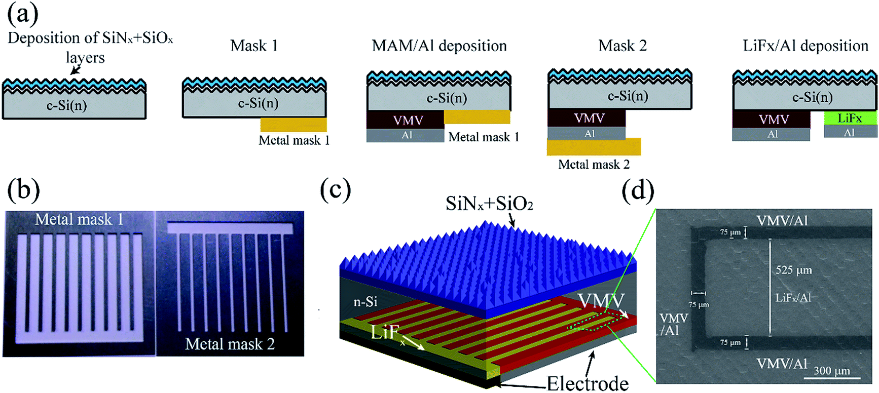 | ||
| Fig. 1 (a) Schematic illustrating the MLBC solar cell metal patterning fabrication process. (b) The two metal patterning masks. (c) The structure of a completed MLBC solar cell. (d) SEM image of the results of metal mask patterning. | ||
The cross-section of VMV/n-Si interfaces were obtained by a focused ion beam (FIB) lift-out technique and observed by FEI Tecnai G2 F30 transmission electron microscopy (TEM) operating at 300 kV. The VMV/n-Si samples were covered with Pd in order to protect the films. The Ultraviolet Photoelectron Spectroscopy (UPS) measurements were performed on Thermo Scientific Escalab 250Xi using the monochromated He I radiation (21.2 eV) in an ultra-high vacuum chamber with a base pressure of 2 × 10⁻⁹ mbar. In order to move surface contaminant, the as-deposited sample was sputtered by Ar+ ions as long as 90 seconds. The UPS spectra were obtained with a sample bias of −5 V in normal emission geometry to obtain secondary electron cutoffs. All spectra were plotted with respect to the Fermi level (EF) determined from the n-Si (100) substrate.
The light J–V behavior was employed on a NewPort system under standard one sun conditions (100 mW cm−2, AM1.5 spectrum, 25 °C) and J–V curves were recorded by Keithley 2400 with a 2 × 2 cm2 aperture mask using a solar simulator (Class AAA, Oriel Sol3A, Newport), and the dark J–V behavior was also investigated. The External Quantum Efficiency (EQE) was conducted using a Solar Cell Quantum Efficiency Measurement System (QEX10, PV Measurements). The JSC of the cell was integrated by the EQE. The injection level dependent open-circuit voltage was measured by transient photo-conductance measurement (WCT-120, Sinton). And the values of contact resistivity ρc for VMV/n-Si contact were respectively measured by the transfer length method (TLM).
3. Results and discussions
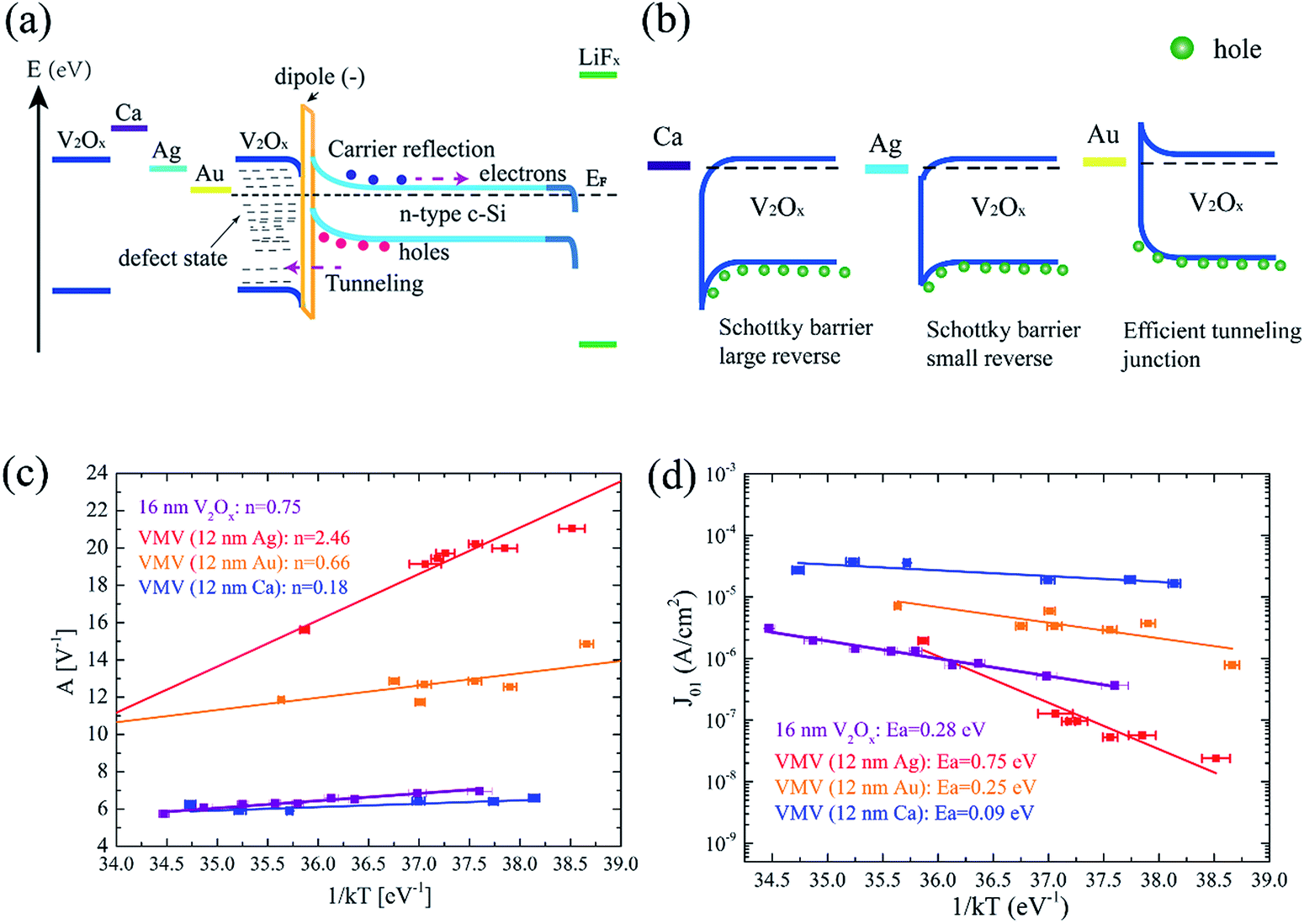
Because the V2Ox (16 nm)/n-Si contact has a relatively low contact resistivity (see Fig. S3†), the top and bottom V2Ox layer thicknesses were both fixed at 8 nm to evaluate the effects of the intermediate metal layer in the VMV emitter systematically. The interfacial morphology, work function, and bulk defect states of the carrier-selective contacts with n-Si play an important role in solar cell performance. The cross-sectional TEM image given in Fig. 2(b) indicates that the interface between the V2Ox and Ag films of the V2Ox/Ag/V2Ox multilayer structure is clearly recognizable, with a structure composed of 7.5 nm thick V2O5, 15 nm thick Ag, and 7.5 nm thick reacted layers consisted of V2O5 and SiOx, respectively, and with an Ag morphology that is clearly identifiable. The interfacial reaction appears during the thermal deposition of V2Ox and causes the surface oxidation of silicon.23 However, when the thickness of the Ag layer is only 4 nm, as shown in Fig. 2(a), some isolated Ag islands are observed to be connected with each other, and the top V2Ox film is mixed with the Ag layer, which exhibits a meandering variation.16 A continuous Ag film can increase the back surface reflectance at long wavelengths, which is beneficial for the performance of MLBC solar cells.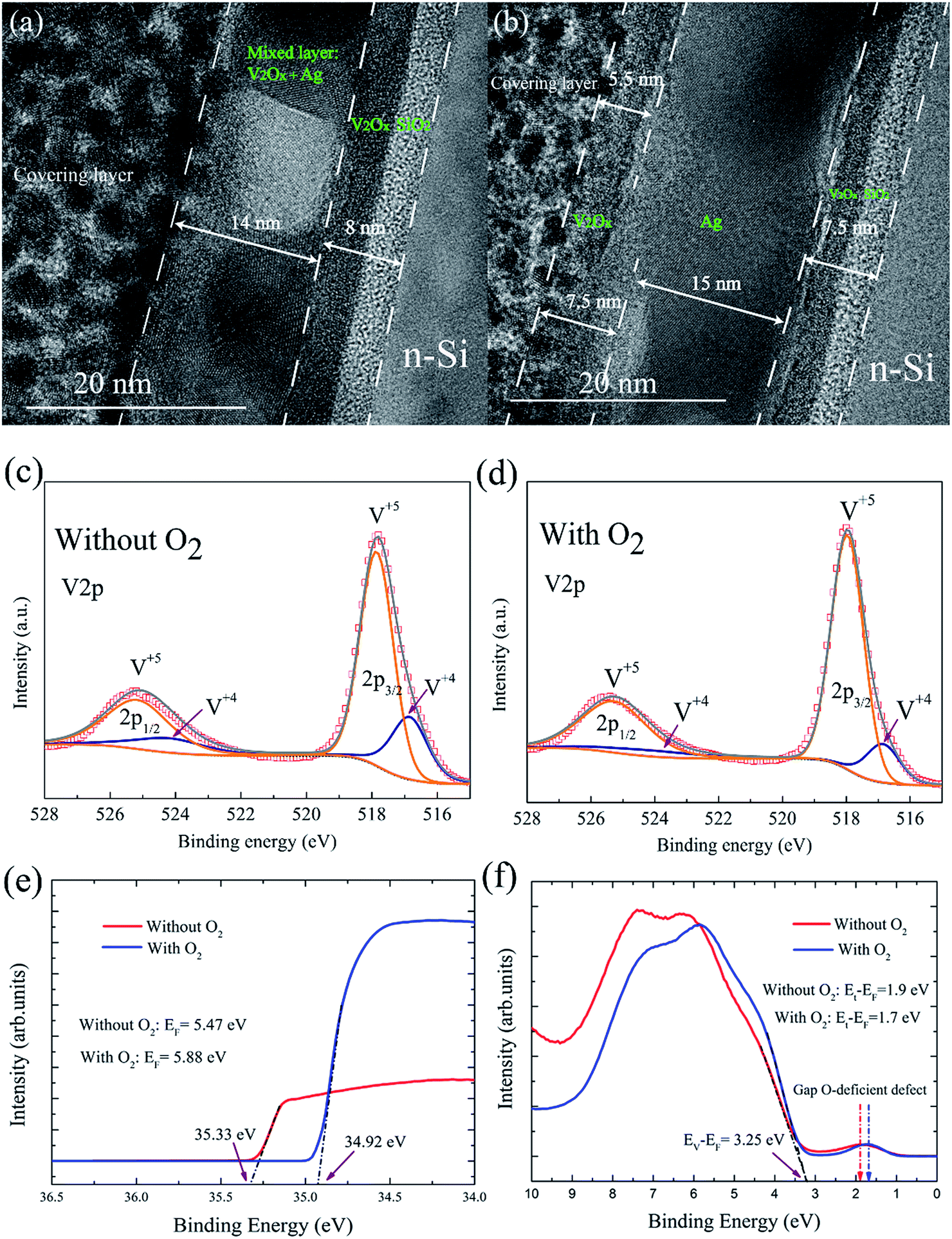 | ||
| Fig. 2 Cross-sectional TEM micrographs of V2Ox (8 nm)/Ag (x nm)/V2Ox (8 nm) multilayer films with (a) x = 4 nm Ag and (b) x = 16 nm Ag. (c) and (d) XPS spectra of V2Ox films prepared without and with the introduction of an O2 partial pressure into the thermal evaporation process, respectively. The UPS spectra of V2Ox films: (e) the work function (EF); (f) shows the positions of the O-deficiency in-gap defect states near the Fermi level. | ||
The V2Ox films were investigated using X-ray photoelectron spectroscopy (XPS) both with and without introducing an O2 partial pressure of 2 × 10⁻² Pa into the evaporation process. Fig. 2(c) and (d) show the 2p1/2 and 2p3/2 spectra indicative of the V5+ and V4+ valence states without and with an introduced O2 partial pressure, respectively. The V4+ valence state, corresponds to an O vacancy at the vertex of an octahedron in the amorphous V2Ox network.24 Based on core level peak areas, the stoichiometry of x = 4.89 and x = 4.84 can be extracted corresponding to V2Ox films with and without O2 partial pressure. It is interesting that the concentration of O vacancies can be reduced when an O2 partial pressure of 2 × 10⁻² Pa is introduced into the evaporation process. The work functions (EF) of the V2Ox films fabricated both with and without introducing an O2 partial pressure of 2 × 10⁻² Pa into the evaporation process were investigated using ultraviolet photoemission spectroscopy (UPS). As shown in Fig. 2(e), the low O vacancy concentrations in the V2Ox film owing to the introduction of an O2 partial pressure leads to a higher work function of 5.88 eV, and also induces greater band bending in the V2Ox/Si junction.12 Furthermore, Fig. 2(f) shows that the energy level (Et) of the O-deficiency in-gap defect state in the bulk of the V2Ox film is transferred from a defect levels (Et − EF = 1.9 eV) to a shallower defect level (Et − EF = 1.7 eV) with the introduction of an O2 partial pressure, which results in reduced bulk recombination in the V2Ox film.12,25 Therefore, the optimized V2Ox films with a high work function and reduced O-deficiency in-gap defect state energy were applied in MLBC solar cells.
Fig. 3 presents the dependence of the characteristic device performance parameters on the thickness of intermediate Ca, Ag, and Au metal layers in VMV multilayer structures, which respectively feature work functions of 2.90 eV,26 4.62 eV and 5.40 eV.27 Fig. 3(a) shows that the average efficiency of MLBC solar cells employing 4 nm Au and 12 nm Ag layers in VMV emitters is improved by 1.20% and 0.78%, respectively. Fig. 3(b) shows that VMV (Ag)-emitter and VMV (Au)-emitter solar cells exhibit only minor differences in the short-circuit current density JSC regardless of the metal layer thickness, and attain values of ∼38 mA cm−2, which are greater than those of MoOx/n-Si front junction solar cells employing excellent interfacial passivation.28 For MLBC solar cells employing VMV (Ag) and VMV (Au) emitters, the FF increases by ∼5% and the VOC values increase by ∼10 mV, as shown in Fig. 3(c) and (d), respectively. However, both the FF and VOC decay for thicker Ag and Au layers. In the case of Au, the FF drastically decreases when thickness of metal increases will be studied in detail below.
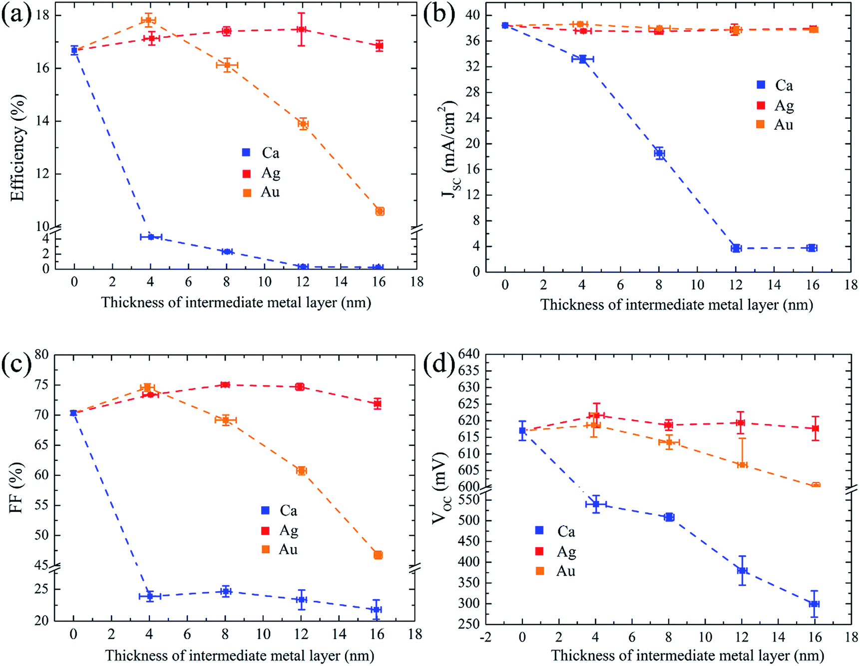 | ||
| Fig. 3 Characteristic performance parameters (efficiency (a), JSC (b), FF (c), and VOC (d)) for the MLBC solar cells fabricated with different intermediate metal layer thicknesses for Ca, Ag, and Au metal layers. | ||
It is of interest that MLBC solar cells employing a low work function Ca layer exhibited an S curve (see Fig. S4†), and uniformly demonstrated relatively poor device performance. In general, however, the FF and JSC are primarily influenced by the value of series resistance RS (see Fig. S4†) and the optical performance for Ca, Ag, and Au layers, which have similar resistivity (∼10−6 Ω cm at 300 K)15 and rear side reflection.27 This indicates that the ultra-low work function of Ca exerts a negative effect on the interfacial carrier transport and contact resistivity of the VMV (Ca)/n-Si contact.
The electrical contact properties and suns–VOC measurements of VMV-based hole-selective contacts with n-Si were characterized, and the results are shown in Fig. 4. As shown in Fig. 4(a), VMV/n-Si contacts generally have lower ρc values compared with the (16 nm) V2Ox/n-Si contact (ρc = 42 mΩ cm2) due to the injection of electrons from the metal layer into the V2Ox layer, which improves its charge carrier concentration. It is worth noting that the averaged ρc values of VMV (12 nm Ag)/n-Si and VMV (4 nm Au)/n-Si are ρc = 1.58 mΩ cm2 and ρc = 0.04 mΩ cm2, respectively. In addition, while the ρc value of VMV (12 nm Au)/n-Si is greater than that of VMV (4 nm Au)/n-Si, the FF corresponding to its use in solar cells is also more than 15% less than that of VMV (4 nm Au)/n-Si solar cells (Fig. 3(c)). However, the VMV (Ca)/n-Si contact exhibits a rectifying characteristic (see Fig. S5†). The physical mechanism by which the VMV (Au) and VMV (Ag) stacks reduce the contact resistivity is not yet clear and further research is needed. Interestingly, Fig. 4(b) shows that the VMV (Au)/n-Si solar cell improves the charge carrier transport dramatically, resulting in an induced p–n junction. A Schottky barrier occurs in V2Ox/n-Si, VMV (4 nm Ag)/n-Si, and VMV (12 nm Ag)/n-Si solar cells with a lowering of the Schottky barrier. In VMV (Ca)/n-Si solar cells, a strong influence of the Schottky contact on the suns–VOC characteristic is observed in the emitter bulk, and generates a voltage opposite to the induced p–n junction voltage, which leads to a reversal in the suns–VOC curve above 10 suns.27
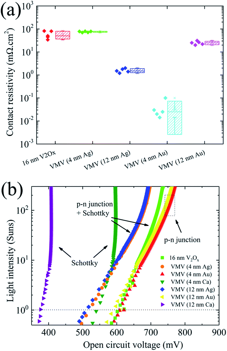 | ||
| Fig. 4 (a) Contact resistivity for different emitter/n-Si contacts. (b) Suns–VOC measurement characteristics for MLBC solar cells featuring various emitter structures. | ||
Fig. 5(a) presents an energy band diagram of an MLBC solar cell in equilibrium, which shows large band bending in n-Si for the extraction of holes at the interface between the n-Si absorber and the bottom V2Ox layer. For the three intermediate layer metals, the work functions of Ca and Ag are much less than that of V2Ox, as shown in Fig. 5(b). The high Schottky barrier and reverse bias of VMV (Ca) interfered with hole transport when used as an emitter for MLBC solar cells, resulting in a low JSC. Furthermore, the quality of interface passivation mainly impacts the high forward-bias voltage (>400 mV) condition, and thus determines the value of VOC.29 Therefore, in this case, we mainly focus on charge carrier transport at the interface under high injection levels, and establish the temperature dependencies of exponential factor A and recombination current density J01 for MLBC solar cells employing VMV (Ag), VMV (Au), and VMV (Ca) emitters. As can be seen from Fig. 5(c), the diffusion–recombination model is dominant at the interface of VMV (Ag)/n-Si and VMV (Au)/n-Si contacts due to the increase in the exponential factor A with increasing 1/kT.29,30 Meanwhile, the multi-tunneling capture emission (MTCE) model determined the charge carrier transport property between V2Ox/n-Si and VMV (Ca)/n-Si contacts at a high forward-bias voltage because the A values remain fairly stable with increasing 1/kT.31 The MTCE process is more related to the bulk recombination in the emitter than to interface defect states, and, thus, the use of VMV (Ca) as an emitter produces a larger recombination rate and lower VOC, as shown in Fig. 3(d). Fig. 5(d) shows the influence of Ca, Ag, and Au metal layers on the emitter bulk recombination mechanism at the VMV/n-Si contact interface of MLBC solar cells. The largest activation energy (Ea = 0.75 eV) obtained for an MLBC solar cell employing a VMV (12 nm Ag) emitter is greater than half the energy gap of n-type c-Si (i.e., Eg/2 = 0.56 eV). Moreover, the value of Ea for an MLBC solar cell employing a VMV (12 nm Au) emitter is close to that of a cell employing a 12 nm V2Ox emitter. Finally, the MLBC solar cell employing a VMV (12 nm Ca) emitter exhibited the lowest value of Ea, which may be explained by the fact that the increased recombination in the VMV (12 nm Ca) emitter bulk is due to the existence of a large Schottky barrier and reverse bias.30 Consequently, the use of a VMV (12 nm Ag) as an emitter in an MLBC solar cell can provides the largest value of Ea (Ea = 0.75 eV) of all the emitters considered, which is also in good agreement with the increased VOC shown in Fig. 3(d).29
 | ||
| Fig. 5 (a) Band diagram for MLBC solar cells and (b) detailed band structures of V2Ox/intermediate metal contacts in VMV emitters. (c) The temperature dependence of the exponential factor (A) for the MLBC solar cells in a high forward-bias voltage (>400 mV) condition. (d) The activation energies (Ea) for each diode extracted from the Arrhenius plots J01 versus 1/kT in the high forward-bias voltage (>400 mV) condition. | ||
Fig. 6(a) shows the J–V curve of an optimized VMV (4 nm Au)/n-Si solar cell with ∼200 Ω sq−1 front surface field passivation (see Fig. S6†), which produce improvement of VOC by 25 mV. The detailed parameters for this optimized MLBC solar cell are listed in Table 1 along with those of other state of the art back-contact dopant-free solar cells for comparison. The MLBC solar cell employing the VMV (4 nm Au) multilayer as the emitter exhibited the highest efficiency of all cells considered, which is 1.44% greater than the efficiency of an optimized MLBC solar cell employing a V2Ox layer as the emitter (with an equivalent FSF). It can be seen from Fig. 6(b) that the IQE is less than 90% for wavelengths greater than 550 nm. This loss is due to electrical shadowing attributed to the recombination of gap and BSF areas, especially, the BSF has a strong impact on the charge collection probability in the base.32 The gap between the emitter layer and back surface field is without any passivation. The surface recombination velocity of the bare silicon is quite high. It would be better to passivate this region in future. Moreover, the moisture and impurities in the air have a substantial effect on the long-term performance of MLBC solar cells, as shown in Fig. 6(c). Here, we note that the efficiency of the optimized MLBC solar cell decreased nearly continuously over a 100 day period in ambient air because the exposure of V2Ox causes the work function to decrease 1 eV until stabilizing.10 Hence, the MLBC solar cell is encapsulated by epoxy resin, which demonstrates a high stability when stored in ambient for greater than 3 months.
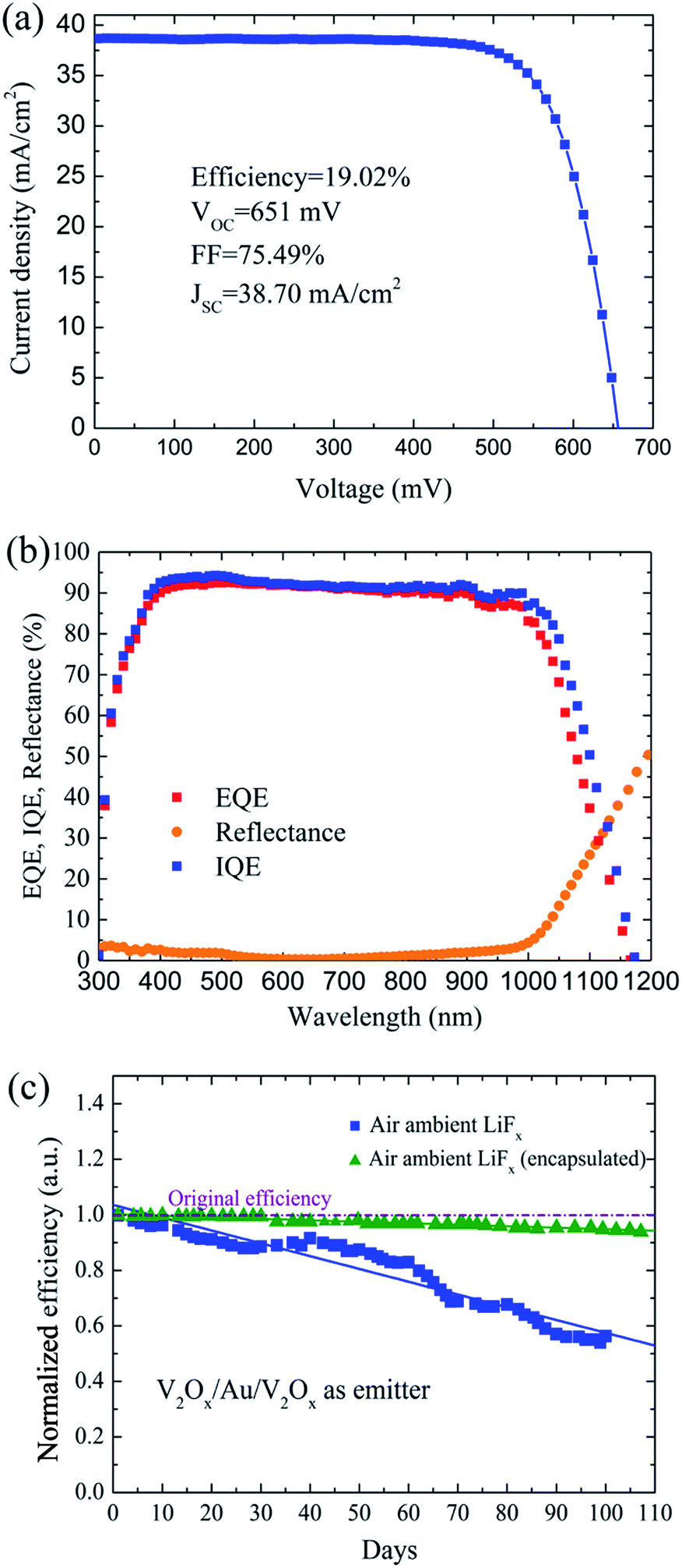 | ||
| Fig. 6 (a) The average J–V response of the best MLBC solar cell employing VMV (4 nm Au) as the hole-selective contact (AM1.5G standard illumination). (b) External quantum efficiency (EQE), internal quantum efficiency (IQE), and reflectance responses. (c) The stability of bare and epoxy resin encapsulated MLBC solar cells employing VMV (4 nm Au) emitters in ambient air. | ||
| Structure | Emitter | BSF | VOC (mV) | JSC (mA cm−2) | FF (%) | η (%) |
|---|---|---|---|---|---|---|
| a Data taken from ref. 9.b Data taken from ref. 5. | ||||||
| Back contact | VMV (4 nm Au) | LiFx | 651 | 38.70 | 75.49 | 19.02 |
| Back contact | 20 nm V2Ox | LiFx | 635 | 38.65 | 71.65 | 17.58 |
| Back contacta | 15 nm V2Ox | Cs2CO3 | 610 | 38.85 | 70.00 | 16.59 |
| Back contactb | 10 nm MoOx | LiFx | 561 | 36.80 | 74.60 | 15.40 |
4. Conclusions
We have developed a novel dopant-free V2Ox/metal/V2Ox multilayer-structured hole-selective contact, which is deposited by thermal evaporation at low-temperature for use in MLBC solar cells. The effect of the choice of metal and the thickness of the intermediate metal layer on the performance of an MLBC solar cell is the most important design criterion, and was therefore subjected to systematic investigation. An optimized MLBC solar cell employing VMV (4 nm Au) as an emitter demonstrated an efficiency of 19.02%, which represents an increase of 1.44% compared to an optimized MLBC solar cell employing a V2Ox/n-Si emitter. Furthermore, MLBC solar cells encapsulated by epoxy resin demonstrated high stability when stored in ambient air. The high performance obtained from MLBC solar cells fabricated using low temperature multilayer film deposition and metal patterning techniques together with the simplicity of the solar cells themselves, suggest the great potential for improving back contact heterojunction silicon solar cells using structured and dopant-free emitters.Acknowledgements
This work was supported by the Guangdong-Hong Kong Technology Cooperation Funding Scheme (Grant No. 2014B050505010), the Guangzhou collaborative innovation Major Project of producing, teaching and researching (Grant No. 201508010011), and the Jiangsu Collaborative Innovation Center of Photovoltaic Science and Engineering (Grant No. SCZ1405500002).References
- A. Ingenito, O. Isabella and M. Zeman, Sol. Energy Mater. Sol. Cells, 2016, 157, 354–365 CrossRef CAS.
- E. Franklin, K. Fong and K. McIntosh, Prog. Photovoltaics, 2014, 24, 411–427 Search PubMed.
- M. Lu, U. Das, S. Bowden, S. Hegedus and R. Birkmire, Prog. Photovoltaics, 2011, 19, 326–338 CAS.
- K. Masuko, M. Shigematsu, T. Hashiguchi, D. Fujishima, M. Kai, N. Yoshimura, T. Yamaguchi, Y. Ichihashi, T. Mishima and N. Matsubara, IEEE J. Photovoltaics, 2014, 4, 1433–1435 CrossRef.
- H.-D. Um, N. Kim, K. Lee, I. Hwang, J. H. Seo and K. Seo, Nano Lett., 2016, 16, 981–987 CrossRef CAS PubMed.
- M. Taguchi, E. Maruyama and M. Tanaka, Jpn. J. Appl. Phys., 2008, 47, 814 CrossRef CAS.
- J. Bullock, M. Hettick, J. Geissbühler, A. J. Ong, T. Allen, C. M. Sutter-Fella, T. Chen, H. Ota, E. W. Schaler, S. D. Wolf, C. Ballif, A. Cuevas and A. Javey, Nat. Energy, 2016, 1, 15031 CrossRef CAS.
- Y. Wan, C. Samundsett, J. Bullock, T. Allen, M. Hettick, D. Yan, P. Zheng, X. Zhang, J. Cui and J. A. McKeon, ACS Appl. Mater. Interfaces, 2016, 8, 14671–14677 CAS.
- W. Wu, J. Bao, X. Jia, Z. Liu, L. Cai, B. Liu, J. Song and H. Shen, Phys. Status Solidi RRL, 2016, 10, 662–667 CrossRef CAS.
- L. G. Gerling, S. Mahato, A. Morales-Vilches, G. Masmitja, P. Ortega, C. Voz, R. Alcubilla and J. Puigdollers, Sol. Energy Mater. Sol. Cells, 2016, 145, 109–115 CrossRef CAS.
- S. M. de Nicolás, J. Coignus, W. Favre, J.-P. Kleider and D. Munoz, Sol. Energy Mater. Sol. Cells, 2013, 115, 129–137 CrossRef.
- M. Mews, L. Korte and B. Rech, Sol. Energy Mater. Sol. Cells, 2016, 158, 77–83 CrossRef CAS.
- J. H. Kim, H.-K. Lee, J.-Y. Na, S.-K. Kim, Y.-Z. Yoo and T.-Y. Seong, Ceram. Int., 2015, 41, 8059–8063 CrossRef CAS.
- H. Han, N. Theodore and T. Alford, J. Appl. Phys., 2008, 103, 013708 CrossRef.
- J.-A. Jeong, Y.-S. Park and H.-K. Kim, J. Appl. Phys., 2010, 107, 023111 CrossRef.
- N. M. Le and B.-T. Lee, Ceram. Int., 2016, 42, 5258–5262 CrossRef CAS.
- L. Cattin, Y. Lare, M. Makha, M. Fleury, F. Chandezon, T. Abachi, M. Morsli, K. Napo, M. Addou and J. C. Bernède, Sol. Energy Mater. Sol. Cells, 2013, 117, 103–109 CrossRef CAS.
- W. Wu, J. Bao, Z. Liu, W. Lin, X. Yu, L. Cai, B. Liu, J. Song and H. Shen, Mater. Lett., 2017, 189, 86–88 CrossRef CAS.
- K. Hong, K. Kim, S. Kim, I. Lee, H. Cho, S. Yoo, H. W. Choi, N.-Y. Lee, Y.-H. Tak and J.-L. Lee, J. Phys. Chem. C, 2011, 115, 3453–3459 CAS.
- J. Bao, W. Wu, Z. Liu and H. Shen, AIP Adv., 2016, 6, 085304 CrossRef.
- L. Shen, Y. Xu, F. Meng, F. Li, S. Ruan and W. Chen, Org. Electron., 2011, 12, 1223–1226 CrossRef CAS.
- A. Tomasi, B. Paviet-Salomon, D. Lachenal, S. M. de Nicolas, A. Descoeudres, J. Geissbühler, S. De Wolf and C. Ballif, IEEE J. Photovoltaics, 2014, 4, 1046–1054 CrossRef.
- K. Kamei, M. Miyachi and K. Tanaka, Phys. Chem. Chem. Phys., 2015, 17, 27409 RSC.
- C. Battaglia, X. Yin, M. Zheng, I. D. Sharp, T. Chen, S. Mcdonnell, A. Azcatl, C. Carraro, B. Ma and R. Maboudian, Nano Lett., 2014, 14, 967–971 CrossRef CAS PubMed.
- M. Bivour, C. Reichel, M. Hermle and S. W. Glunz, Sol. Energy Mater. Sol. Cells, 2012, 106, 11–16 CrossRef CAS.
- T. G. Allen, J. Bullock, P. Zheng, B. Vaughan, M. Barr, Y. Wan, C. Samundsett, D. Walter and A. Javey, Prog. Photovoltaics, 2016 DOI:10.1002/pip.2838.
- M. Bivour, C. Reichel, M. Hermle and S. W. Glunz, Sol. Energy Mater. Sol. Cells, 2012, 106, 11–16 CrossRef CAS.
- J. Geissbühler, J. Werner, S. M. De Nicolas, L. Barraud, A. Hessler-Wyser, M. Despeisse, S. Nicolay, A. Tomasi, B. Niesen and S. De Wolf, Appl. Phys. Lett., 2015, 107, 081601 CrossRef.
- T. Schulze, L. Korte, E. Conrad, M. Schmidt and B. Rech, J. Appl. Phys., 2010, 107, 023711 CrossRef.
- V. A. Dao, Y. Lee, S. Kim, Y. Kim, N. Lakshminarayan and J. Yi, J. Electrochem. Soc., 2011, 158, H312–H317 CrossRef CAS.
- Y. J. Song, M. Park, E. Guliants and W. A. Anderson, Sol. Energy Mater. Sol. Cells, 2000, 64, 225–240 CrossRef CAS.
- C. Reichel, F. Granek, M. Hermle and S. Glunz, J. Appl. Phys., 2011, 109, 024507 CrossRef.
Footnote |
| † Electronic supplementary information (ESI) available. See DOI: 10.1039/c7ra03368k |
| This journal is © The Royal Society of Chemistry 2017 |