
 Open Access Article
 This Open Access Article is licensed under a
 Creative Commons Attribution 3.0 Unported Licence
Colloidal synthesis and characterization of single-crystalline Sb2Se3 nanowires†
Yike Liu ab,
Yaqin Tanga,
Ying Zenga,
Xun Luoa,
Jingyu Rana,
Yongmei Luoa,
Xiangdong Sua,
Boon K. Ngc,
Fangyang Liu*b and
Liangxing Jiang*b
ab,
Yaqin Tanga,
Ying Zenga,
Xun Luoa,
Jingyu Rana,
Yongmei Luoa,
Xiangdong Sua,
Boon K. Ngc,
Fangyang Liu*b and
Liangxing Jiang*b
aSchool of Material and Metallurgical Engineering, Guizhou Institute of Technology, Guiyang 550003, China
bSchool of Metallurgy and Environment, Central South University, Changsha 410083, China. E-mail: liufangyang@csu.edu.cn
cFaculty of ESTeM, University of Canberra, Bruce, ACT 2601, Australia
First published on 5th May 2017
Abstract
In the present study, single-crystalline Sb2Se3 nanowires have been synthesized by a hot-injection method. The crystal structure of the prepared Sb2Se3 nanowires has been comprehensively characterized by a series of techniques, namely X-ray diffraction (XRD), Raman spectroscopy, transmission electron microscopy (TEM) as well as selected area electron diffraction (SAED). The mechanism of formation of amorphous phase and nanowires has also been intensively investigated. It is evident that the formation of Sb2Se3 nanowires strongly depends on the reaction temperature. A band gap of 1.06 eV for Sb2Se3 nanowires has been ascertained from UV-vis-NIR measurements. Moreover, coated film consisting of Sb2Se3 nanowires demonstrates a clear photoresponse in photoelectrochemical measurements. This work has conclusively demonstrated that Sb2Se3 nanowires have great potential in solar energy conversion.
Introduction
Antimony selenide (Sb2Se3), one of the most important metal selenides, is an intriguing functional material owing to its outstanding applicability spanning the photovoltaic,1–5 optoelectronic,6–8 photothermal,9 and thermoelectric10 fields. Sb2Se3 has a broad absorption range in the visible spectrum (absorption coefficient > 105 cm−1) with a suitable band gap of ∼1.0 eV, making it an emerging candidate for photovoltaics.2,11 On top of this, Sb2Se3 is relatively earth-abundant and nontoxic, and is cost-effective yet environmentally friendly.1,5In recent years, the use of nanostructured precursors in the fabrication of thin films for solar cell applications has gained popularity.12,13 Compared with conventional physical vapor deposition methods, solution-based routes are associated with lower fabrication costs as well as high-quality nanocrystals including nanoparticles, nanowires and nanosheets leading to high power conversion efficiency.14 Hot-injection is an excellent solution-based route, which can exhibit better control of nanocrystal morphology and size within a short reaction time.15 This technique has been widely employed for the preparation of numerous monodisperse colloidal nanocrystals.
However, investigations on the synthesis of single-crystalline Sb2Se3 nanowires via the hot-injection method have scarcely been reported until recently. In 2009, Deng et al. first reported the synthesis of Sb2Se3−xSx (0 < x < 3) nanotubes via a hot-injection method in paraffin liquid,16 and an extension of this work was published in 2014. Choi and coworkers also studied the synthesis of Sb2Se3 nanowires via injection of antimony precursor into hot solvent comprising selenium powder and surfactant.17 Sb2Se3 nanorods were then prepared using a similar process.18 However, the reactivity of Se-octadecene suspension has been found to be problematic as it exerted a negative impact on nanocrystal quality.19,20 Recently, fabrication of ultralong Sb2Se3 nanowires has been successfully accomplished via an organometallic synthesis by reacting triphenylantimony(III) with dibenzyldiselenide.9 The major drawback of this synthesis process, however, is that dibenzyldiselenide is a hazardous, expensive and environmentally harmful Se precursor. Therefore, a facile, environmentally friendly and more effective method for the synthesis of high quality and uniform single-crystalline Sb2Se3 nanowires is highly desired.
Consequently, this work focuses on the synthesis of Sb2Se3 nanowires through a facile and green hot-injection method using oleylamine (OLA). In this process, a solution consisting of Se–dimethylamine borane (DMAB)–OLA was used as a phosphine-free and highly active Se precursor, as reported in our previous works.21–23 The structure, morphology, composition and absorptivity of the products were comprehensively characterized using different methods. In addition, the photoresponse of Sb2Se3 nanowires was studied using photoelectrochemical measurements and the potential for solar energy conversion is discussed.
Experimental
Syntheses of Sb2Se3 nanowires were carried out utilizing a hot-injection method via a standard air-inert Schlenk line. In a typical synthesis, the Se powder was completely dissolved in OLA at 110 °C with the assistance of DMAB as a co-solvent, to give a Se–DMAB–OLA solution. The Se–DMAB–OLA solution was then quickly injected into a hot solution containing antimony chloride at 180 °C for 30 min under an Ar atmosphere. Full experimental details can be found in the ESI.†Results and discussion
Electron microscopy was conducted to characterize the morphology and structural integrity of the nanowires. Fig. 1 shows representative transmission electron microscopy (TEM) images for the Sb2Se3 nanowires. According to the TEM images (Fig. 1(a) and (b)), each nanowire had a diameter of 40–60 nm with a typical length of several micrometers (additional SEM images can be found in the ESI†). Fig. 1(c) demonstrates that the lattice spacing of Sb2Se3 nanowire was ca. 3.25 and 3.28 Å. This corresponds to the lattice spacing of the (230) and (021) planes, respectively, for Sb2Se3 with orthorhombic geometry. The SAED pattern, as shown in Fig. 1(d), indicates that Sb2Se3 nanowires are single-crystalline. All of these results revealed that the structural integrity of Sb2Se3 nanowires is preferentially oriented along the [001] direction, which is coincident with previous studies on Sb2Se3 nanowires and nanorods.7,24–27 | ||
| Fig. 1 (a and b) Low resolution TEM images of Sb2Se3 nanowires. (c) High resolution TEM image showing interplanar spacing of 3.25 Å, 3.28 Å and 3.53 Å. (d) SAED pattern indexed to Sb2Se3. | ||
X-ray diffraction (XRD) was used to further ascertain the crystal structure of the Sb2Se3 nanowires. Fig. 2(a) displays the XRD pattern of the synthesized sample. It can be seen that the obtained sample is composed of an orthorhombic phase Sb2Se3 (JCPDS 72-1184). Seven major peaks, namely at 2θ = 16.911°, 27.439°, 28.130°, 31.127°, 32.280°, 34.124° and 35.584° corresponding to (120), (230), (211), (221), (301), (240) and (231), respectively, have been fingerprinted. No evidence of other impurities such as Sb2O3, Sb, etc. was found in the respective XRD pattern. The ratio of the compositional elements determined by energy dispersive spectroscopy (EDS) was Sb/Se: 2.00![[thin space (1/6-em)]](https://www.rsc.org/images/entities/char_2009.gif) :2.88, implying that the composition of the Sb2Se3 nanowires is close to the stoichiometry of Sb2Se3 (see the ESI, Fig. S3†). To further validate the phase and purity of the obtained product, Raman spectroscopy and X-ray photoelectron spectroscopy (XPS) have been used. In the Raman spectrum (Fig. 2(b)), the peaks at 190 cm−1 and 253 cm−1 are coincident with previous investigations of Sb2Se3 nanostructures.24,28 The results of XPS further demonstrated that both Sb and Se elements are in their expected oxidation states (see the ESI, Fig. S4(a)–(c)†).24,29 The XRD, Raman and XPS data have demonstrated that the synthesized nanowires are native orthorhombic phase Sb2Se3.
:2.88, implying that the composition of the Sb2Se3 nanowires is close to the stoichiometry of Sb2Se3 (see the ESI, Fig. S3†). To further validate the phase and purity of the obtained product, Raman spectroscopy and X-ray photoelectron spectroscopy (XPS) have been used. In the Raman spectrum (Fig. 2(b)), the peaks at 190 cm−1 and 253 cm−1 are coincident with previous investigations of Sb2Se3 nanostructures.24,28 The results of XPS further demonstrated that both Sb and Se elements are in their expected oxidation states (see the ESI, Fig. S4(a)–(c)†).24,29 The XRD, Raman and XPS data have demonstrated that the synthesized nanowires are native orthorhombic phase Sb2Se3.
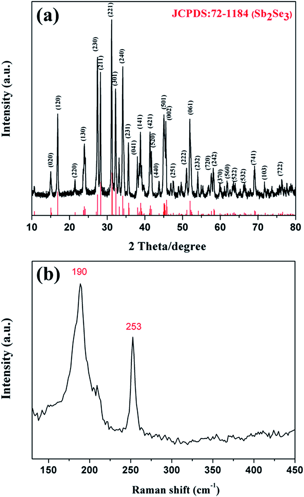 | ||
| Fig. 2 (a) XRD pattern and (b) Raman spectrum of the as-synthesized Sb2Se3 nanowires. | ||
To study the crystal growth mechanism of the Sb2Se3 nanowires, the morphology and structure of the reaction products at different reaction times were monitored by TEM and XRD, as graphed in Fig. S5 and S6 (included in ESI†). During the initial phase (1 min), some amorphous materials were observed. As the reaction moved forward (2, 4, 8 min), these amorphous materials then clustered into nanowires indicating that the nanowires may nucleate around the amorphous matrix. With a reaction time of just 16 min, the amorphous materials had been depleted to entirety, forming nanowires. The peaks in the corresponding XRD pattern suggest that the proposed product was indeed a pure Sb2Se3. From the above-mentioned results, a probable formation route can be conjectured as follows: antimony trichloride was dissolved in oleylamine to form a Sb3+–OLA complex initially followed by introduction into the resulting solution. The Se–DMAB–OLA solution was then injected into the hot-injection medium. Se2− was the product from the reduction of Se powders by DMAB followed by reaction with OLA to form OLAmSen. The Sb2Se3 nuclei were then formed via homogeneous nucleation. As the reaction moved forward, these Sb2Se3 crystal nuclei rapidly aggregated into irregular particles where nanowires nucleated via the Ostwald ripening process. When the reaction was extended, it resulted in the formation of uniform Sb2Se3 nanowires. OLA has been successfully employed with a dual role (solvent and surfactant) in the synthesis of Sb2Se3 nanowires. Previous investigation has demonstrated that OLA can efficiently modify and stabilize the surface of the Sb2Se3 nanoparticles, resulting in the formation of the Sb2Se3 nanowires by oriented aggregation.24 In this reaction, the OLA was adsorbed onto the surface of the Sb2Se3 nanowires (mainly on (hk0)) based on the structural determination, and this further enhanced the anisotropic growth of the Sb2Se3 nanowires.
The formation of pure Sb2Se3 nanowires was found to be highly dependent on the reaction temperature. Experiments with various reaction (injection) temperatures have been trialled (see the ESI, Fig. S7†): the products at lower reaction temperature (160 °C) were predominantly in an amorphous phase. When the reaction temperature was below 160 °C, the reaction was slow and incomplete. Higher temperature (200 °C) injection and reaction led to the product containing significant elementary Sb. Kinetically, it has been found that higher temperatures increase the probability for successful nucleation.30 When the reaction temperature was over 200 °C, elementary Sb that was observed from the experiment could be attributed to the reduction of antimony precursors. OLA has been demonstrated to serve as a surfactant as well as a reductant for the synthesis of various nanocrystal systems at appropriate temperatures.31,32 It has been proposed that OLA might act as a ligand to form stable complexes with Sb3+ while heating (high temperature) induces the thermolytic reduction of Sb complexes to elementary Sb in the reaction. Similar phenomena were found in our previous works for the synthesis of Cu3BiS3 nanocrystals.33 The synthesis procedure should be carried out at various temperatures ranging from 170 to 190 °C and the reaction can proceed with elevation of the reaction temperature.
Multiple antimony precursors were also examined. Antimony triacetate was found to reproducibly result in pure Sb2Se3 nanowires. The concentrations of both Sb and Se were also found to be critical in achieving pure samples. It is important to note that when the Sb/Se ratio was 1:1.5 at different temperatures, significant Sb2O3 impurity has been observed in the XRD data (see the ESI, Fig. S8†). The use of excess Se was deemed to be necessary to balance out the cationic precursors in order to avoid side reactions. During a series of trials, the injection quantities of Se were also varied and evaluated where the reaction temperature remained unchanged at 190 °C (see the ESI for details, Fig. S9†). For mole ratios of Sb/Se at 1:1.7, pure Sb2Se3 nanowires were formed.
The absorptivity of the synthesized Sb2Se3 nanowires was measured using UV-vis-NIR absorbance spectroscopy and is illustrated in Fig. 3. The spectrum presents a slow, monotonic rise in absorption. The band gap of the Sb2Se3 nanowires has been determined to be 1.06 eV by extrapolating the linearity in the plot of absorbance squared versus energy as shown in the inset in Fig. 3. The value is in good agreement with the literature value for bulk Sb2Se3.34 The obtained band gap value for our Sb2Se3 nanowires is close to the optimal value suited for solar cell application.35
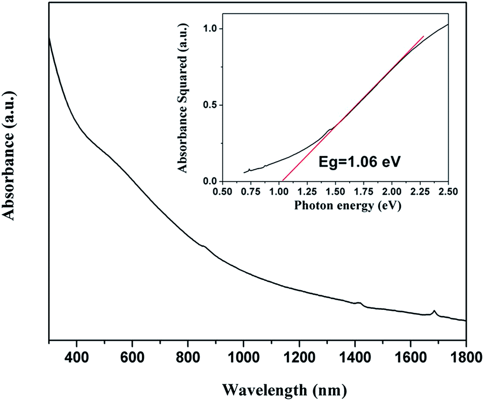 | ||
| Fig. 3 UV-vis-NIR absorption spectrum of the as-synthesized nanowires. Inset shows the absorbance2 vs. eV for Sb2Se3 nanowires; the estimated band energy is 1.06 eV. | ||
In order to further evaluate the applicability of this material for photoelectrical conversion applications, the photo-responsiveness of Sb2Se3 nanowires was measured in a photoelectrochemical cell (PEC). The Sb2Se3 nanocrystal-ink was coated directly onto indium tin oxide (ITO) glass substrate (which served as work electrodes) by the drop-casting method, forming a nanocrystalline thin film. This film was mounted onto a traditional three-electrode photoelectrochemical cell with a graphite counter electrode relative to a saturated calomel reference electrode (SCE) containing 0.5 M H2SO4. The incident light intensity was 100 mW cm−2, and a biased voltage of −0.4 V vs. SCE was applied. Fig. 4(a) displays the current density versus potential (vs. SCE) plots for the prepared Sb2Se3 nanowire films utilizing a chopping method (10 s light on, 10 s light off). The photocurrent density increased with a negative shift in cathodic potential, which is a typical characteristic of a p-type semiconductor for a Sb2Se3 nanowire film. The photocurrents for Sb2Se3 nanowire films increased significantly with increasing negative bias reaching up to ∼6 μA cm−2 at −0.4 V. The value is almost on par with a previous report where the Sb2Se3 film was fabricated by an electrochemical deposition process.8 However, our finding shows a much lower value than that obtained from the reported Sb2Se3 film formed from annealing treatment and optimization of the coating process.7 It has been concluded that the annealing treatment can effectively modify the morphology and structural integrity of the Sb2Se3 nanocrystals and remove the undesirable residual phases.
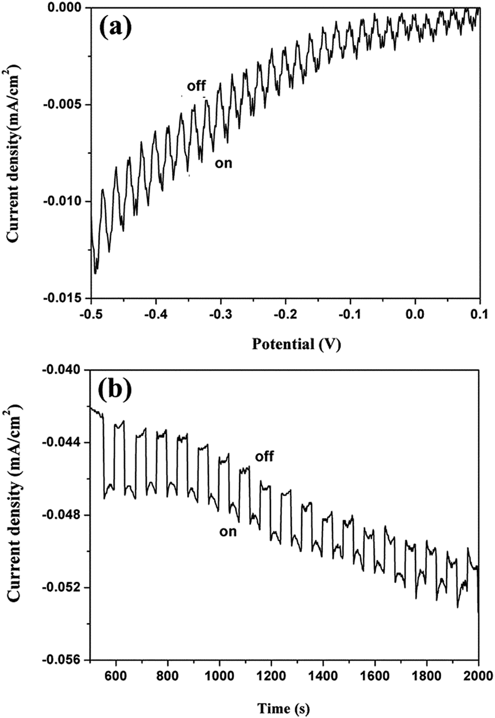 | ||
| Fig. 4 (a) Photocurrent–potential plot of the Sb2Se3 films on an ITO substrate in 0.5 M H2SO4 under 100 mW cm−2 illumination. (b) The transient photocurrent spectrum at −0.4 V vs. SCE. | ||
The transient I–V spectrum at −0.4 V is depicted in Fig. 4(b). The measured photocurrent values were between 3 and 5 μA cm−2, which remained constant consistently and reproducibly over 18 cycles. This has demonstrated the competent photoresponse and photostability of the Sb2Se3 nanowire film. It also indicates the applicability of Sb2Se3 nanowires and/or the corresponding thin film in the field of solar energy conversion.
Conclusions
In this study, a colloidal synthesis of single-crystalline Sb2Se3 nanowires via a hot-injection method has been presented. Sb2Se3 nanowires with a diameter of 40–60 nm and a typical length of several micrometers have been observed. The structural integrity of the synthesized Sb2Se3 nanowires has been evaluated by a number of methods including HRTEM, SAED, XRD and Raman spectroscopy. The results of EDS have confirmed the composition of the Sb2Se3 nanowires in the sample. A probable formation route has been proposed from the evolution of the morphologies and phases. The reaction temperature has also been found to play a crucial role in determining the phase of the synthesized nanocrystals. The use of antimony triacetate as precursor has also been observed to be instrumental in yielding phase pure Sb2Se3 nanowires at an appropriate ratio (Sb/Se = 1:1.7) and at 190 °C. The band gap of 1.06 eV for Sb2Se3 nanowires has been determined by UV-vis-NIR data. The PEC tests have also demonstrated that Sb2Se3 nanowire films have a good photoresponse in the range 3 to 5 μA cm−2 without any optimization. Our work has conclusively demonstrated that the synthesized Sb2Se3 nanowires have great potential in solar energy conversion.
Acknowledgements
This work was supported by the National Natural Science Foundation of China (Grant No. 51604088) and the National Natural Science Foundation of Guizhou Province (Qian Ke He LH[2015]7091) as well as the High Qualified People Starting Foundation of GIT (XJGC20161236).Notes and references
- Y. Zhou, L. Wang, S. Y. Chen, S. K. Qin, X. S. Liu, J. Chen, D. J. Xue, M. Luo, Y. Z. Cao, Y. B. Cheng, E. H. Sargent and J. Tang, Nat. Photonics, 2015, 9, 409–415 CrossRef CAS.
- X. S. Liu, C. Chen, L. Wang, J. Zhong, M. Luo, J. Chen, D. J. Xue, D. B. Li, Y. Zhou and J. Tang, Prog. Photovoltaics, 2015, 23, 1828–1836 CAS.
- Y. Zhou, M. Y. Leng, Z. Xia, J. Zhong, H. B. Song, X. S. Liu, B. Yang, J. P. Zhang, J. Chen, K. H. Zhou, J. B. Han, Y. B. Cheng and J. Tang, Adv. Energy Mater., 2014, 4, 1301846 CrossRef.
- Y. C. Choi, T. N. Mandal, W. S. Yang, Y. H. Lee, S. H. Im, J. H. Noh and S. I. Seok, Angew. Chem., Int. Ed., 2014, 53, 1329–1333 CrossRef CAS PubMed.
- K. Zeng, D.-J. Xue and J. Tang, Semicond. Sci. Technol., 2016, 31, 063001 CrossRef.
- B. R. Sankapal and C. D. Lokhande, Sol. Energy Mater. Sol. Cells, 2001, 69, 43–52 CrossRef CAS.
- J. Kim, W. Yang, Y. Oh, H. Lee, S. Lee, H. Shin, J. Kim and J. Moon, J. Mater. Chem. A, 2017, 2180–2187 CAS.
- J. Yang, Y. Lai, Y. Fan, Y. Jiang, D. Tang, L. Jiang, F. Liu and J. Li, RSC Adv., 2015, 5, 85592–85597 RSC.
- G. Chen, J. Zhou, J. Zuo and Q. Yang, ACS Appl. Mater. Interfaces, 2016, 8, 2819–2825 CAS.
- I. H. Kim, Mater. Lett., 2000, 43, 221–224 CrossRef CAS.
- M. R. Filip, C. E. Patrick and F. Giustino, Phys. Rev. B: Condens. Matter Mater. Phys., 2013, 87, 205125 CrossRef.
- C. N. Bucherl, K. R. Oleson and H. W. Hillhouse, Curr. Opin. Chem. Eng., 2013, 2, 168–177 CrossRef.
- Q. Guo, S. J. Kim, M. Kar, W. N. Shafarman, R. W. Birkmire, E. A. Stach, R. Agrawal and H. W. Hillhouse, Nano Lett., 2008, 8, 2982–2987 CrossRef CAS PubMed.
- H. W. Hillhouse and M. C. Beard, Curr. Opin. Colloid Interface Sci., 2009, 14, 245–259 CrossRef CAS.
- C. D. Donega, P. Liljeroth and D. Vanmaekelbergh, Small, 2005, 1, 1152–1162 CrossRef PubMed.
- Z. T. Deng, M. Mansuripur and A. J. Muscat, Nano Lett., 2009, 9, 2015–2020 CrossRef CAS PubMed.
- D. Choi, Y. Jang, J. Lee, G. H. Jeong, D. Whang, S. W. Hwang, K. S. Cho and S. W. Kim, Sci. Rep., 2014, 4, 6714 CrossRef CAS PubMed.
- C. Zhang, Z. Li, Y. Guo, X. Niu, X. Liang, D. Zhou, H. Zhu, J. Chen and Y. Mai, J. Nanosci. Nanotechnol., 2017, 17, 1338–1344 Search PubMed.
- C. Bullen, J. van Embden, J. Jasieniak, J. E. Cosgriff, R. J. Mulder, E. Rizzardo, M. Gu and C. L. Raston, Chem. Mater., 2010, 22, 4135–4143 CrossRef CAS.
- J. Jasieniak, C. Bullen, J. van Embden and P. Mulvaney, J. Phys. Chem. B, 2005, 109, 20665–20668 CrossRef CAS PubMed.
- Y. K. Liu, J. Yang, E. N. Gu, T. T. Cao, Z. H. Su, L. X. Jiang, C. Yan, X. J. Hao, F. Y. Liu and Y. X. Liu, J. Mater. Chem. A, 2014, 2, 6363–6367 CAS.
- Y. K. Liu, M. M. Hao, J. Yang, L. X. Jiang, C. Yan, C. Huang, D. Tang, F. Y. Liu and Y. X. Liu, Mater. Lett., 2014, 136, 306–309 CrossRef CAS.
- Y. K. Liu, F. Y. Liu, C. Huang, X. J. Lv, Y. Q. Lai, J. Li and Y. X. Liu, Mater. Lett., 2013, 108, 110–113 CrossRef CAS.
- G. Chen, W. Wang, C. Wang, T. Ding and Q. Yang, Adv. Sci., 2015, 2, 1500109 CrossRef PubMed.
- R. Jin, G. Chen, J. Pei, J. Sun and Y. Wang, Nanoscale, 2011, 3, 3893–3899 RSC.
- T. Zhai, M. Ye, L. Li, X. Fang, M. Liao, Y. Li, Y. Koide, Y. Bando and D. Golberg, Adv. Mater., 2010, 22, 4530–4533 CrossRef CAS PubMed.
- J. Ma, Y. Wang, Y. Wang, P. Peng, J. Lian, X. Duan, Z. Liu, X. Liu, Q. Chen, T. Kim, G. Yao and W. Zheng, CrystEngComm, 2011, 13, 2369–2374 RSC.
- Y. Q. Liu, M. Zhang, F.-X. Wang and G.-B. Pan, J. Mater. Chem. C, 2014, 2, 240–244 RSC.
- J. Wang, Z. Deng and Y. Li, Mater. Res. Bull., 2002, 37, 495–502 CrossRef CAS.
- J. van Embden and P. Mulvaney, Langmuir, 2005, 21, 10226–10233 CrossRef CAS PubMed.
- S. Mourdikoudis and L. M. Liz-Marzán, Chem. Mater., 2013, 25, 1465–1476 CrossRef CAS.
- Z. Xu, C. Shen, Y. Hou, H. Gao and S. Sun, Chem. Mater., 2009, 21, 1778–1780 CrossRef CAS.
- C. Yan, E. Gu, F. Liu, Y. Lai, J. Li and Y. Liu, Nanoscale, 2013, 5, 1789–1792 RSC.
- Y. Rodriguez-Lazcano, Y. Pena, M. T. S. Nair and P. K. Nair, Thin Solid Films, 2005, 493, 77–82 CrossRef CAS.
- A. Goetzberger, C. Hebling and H.-W. Schock, Mater. Sci. Eng., R, 2003, 40, 1–46 CrossRef.
Footnote |
| † Electronic supplementary information (ESI) available. See DOI: 10.1039/c7ra03319b |
| This journal is © The Royal Society of Chemistry 2017 |