
 Open Access Article
 This Open Access Article is licensed under a
 Creative Commons Attribution 3.0 Unported Licence
A novel MoS2-based hybrid film as the back electrode for high-performance thin film solar cells†
Sheng Yuan,
Ming-Jian Zhang,
Xiaoyang Yang,
Zongwei Mei,
Yongji Chen and
Feng Pan *
*
School of Advanced Materials, Peking University Shenzhen Graduate School, Shenzhen, 518055, China. E-mail: panfeng@pkusz.edu.cn
First published on 27th April 2017
Abstract
MoS2, a representative two-dimensional transition metal dichalcogenide, gains significant interest due to its unique layered structure and electronic structure. In this work, a novel MoS2-based hybrid thin film was constructed by disordered stacking of MoS2–NMP hybrid particles, which were mainly composed of MoS2(NMP)3 molecules stacking in a nearly-parallel manner through S⋯H–C hydrogen bonds. Interestingly, it presents a higher work function (5.42 eV) than Au (5.32 eV), and a unique thickness-dependent conductivity with p-type semiconductor characteristic. Using it as the back contact of CdTe solar cells, the efficiency was improved by 2.6% compared to the traditional cells, mainly from the great improvement in short-circuit current density (Jsc). This significant improvement in solar performance was ascribed to the matchable energy levels at the CdTe/MoS2-based thin film interface and its unique thickness-dependent conductivity. This work opens a new direction for the extensive applications of TMD-based materials.
Introduction
Recently, two-dimensional transition metal dichalcogenides (TMD), such as MoS2, WS2, WSe2, etc.,1–4 have gained significant interest, because of their impressive electronic, photonic and chemical properties, and large natural abundance.2,4–7 As a typical representative, MoS2 has been widely applied in solar cells, photocatalytic, electrocatalytic, biosystems and photodetector devices.7–13 The great popularity of MoS2 not only depends on its intrinsic bulk properties, but also significantly depends on its tunable electronic properties due to its unique crystal structure. In a representative hexagonal structure (P63/mmc), Mo and S atoms are covalently bonded in S–Mo–S molecular layers, which stack together via weak van der Waals (vdW) interactions along the z axis to form the bulk material. The strong intra-layer and weak inter-layer interactions bring with the high anisotropy of MoS2, which also make it possible to exfoliate the bulk MoS2 into few layers, even single layer. With the dimension decrease from 3D to 2D, the band gaps, electronic structures and work functions of MoS2 greatly vary. For example, the band structures are significantly changed from an indirect band gap of 1.29 eV to a direct band gap of 1.90 eV as we thin down the 2D layers to the single-layer limit.14 So 2D TMDs provide a great platform of tuning material properties towards desired functions, further attracting a great deal of attention and opening up opportunities for a wide range of applications.Cadmium telluride (CdTe) solar cells have taken a largest market share in all compound thin film solar cells because of the low cost, high efficiency, long-term stability, and large-scale applications. Nevertheless, there are still many problems to hinder its efficiency improvement. The significant one is the issue of the back contact owing to the high work function (5.7 eV) and high electron affinity (4.5 eV) of CdTe.15–17 Commonly used metal thin films, such as Ag, Al, and etc., own lower work function than that of CdTe, and could not directly match with CdTe layer to construct a good ohmic contact. To solve this problem, various materials with high work functions are used as the back contact, such as MoO3,18,19 Sb2Te3,20,21 V2O5,17 HgTe,16 etc. Our group has devoted a lot of efforts to searching for new back contact materials. And a series of materials, such as ALD–Al2O3, CuAlOx and Cu9S5, were found to be beneficial to improve the efficiency.22–24 Because MoS2 exhibits layer-number-dependent electronic structure and work functions, we predict that few layers or single layer of MoS2 might be a potential candidate for the back contact material to implement a good ohmic contact and the efficiency improvement.
In this work, we tried to fabricate single layer or few layers of MoS2 by liquid phase exfoliating method at first,9,25 but unexpectedly discovered that MoS2 can be dissolved in N-methyl-2-pyrrolidone (NMP). So a novel MoS2-based hybrid thin film was found for the first time, which was fabricated by spin-coating and subsequent thermal treatment as a new back contact material for CdTe thin-film solar-cells. Interestingly, it was found to be a p-type semiconductor thin film with higher work function (5.42 eV) than Au with tunable conductivity with thickness. When applied it as the back contact in CdTe solar cell, a short-circuit current density (Jsc) improvement, by 3.7 mA cm−2 than the traditional cells, was implemented, which brought with a great efficiency improvement of 2.6%. After a careful and systematical study, this great improvement could be ascribed to the high work function of MoS2-based complex thin film with the matching energy level structures between it and CdTe layer for enhancing Jsc. This work not only provides a new and effective material system for the efficiency improvement of solar cells, but also opens a new research direction for the applications of TMDs.
Experimental procedures
Preparation of MoS2–NMP solution
0.5 g of MoS2 powders (99.9%, Aladdin) was added into 40 mL N-methyl-2-pyrrolidone solvent (NMP, 99.9%, Aladdin). The mixture was stirred to dissolve at 70 °C for 12 h. Then the suspension was centrifuged at 8000 rpm for 15 minutes. We gained black precipitate and faint yellow solution (MoS2–NMP solution). Faint yellow solution was collected and used to fabricate the back contact of CdTe solar cells. Solution was further verified by nanometer particle size analyzer, which can distinguish the minimum size of particle is 0.3 nm. No nanometer particle was detected in the solution.Fabrication of CdTe solar cells
Commercial soda lime glass substrates coated with fluorine-doped tin oxide (FTO-glass) was purchased, which had a sheet resistance of 35 Ω sq−1 and a transmittance of about 85%. Then they were cleaned in an ultrasonic bath using de-ionized water and acetone. About 100 nm-thick CdS window layer was deposited on FTO-glass by radio frequency magnetron sputtering using argon gas with a 4N purity (99.99%). CdTe layers were deposited via close space sublimation (CSS). CdTe source and substrate was under 650 °C and 580 °C, respectively. A thickness of about 4 μm for CdTe layer was gained. To encourage CdTe grains growth, passivate grain boundaries of CdTe and improve the CdS/CdTe interface,26–28 CdCl2 treatment was performed. Samples were soaked in a 70%-saturated CdCl2 methanol solution for 15 minutes. Then they were annealed at 390 °C for 30 minutes. In order to CdTe form Te-rich layer on the surface of CdTe layer, samples were etched with nitric-phosphoric acid for 30 s. Following etching treatment, a 3 nm-thick Cu layer was evaporated on Te-rich layer by vacuum evaporation. Then MoS2–NMP solution was spin-coated on Cu layer surface, following by a thermal treatment on hot plate at 200 °C. Then samples were annealed under 150 °C for 30 minute. Finally an Au back electrode with thickness of 30 nm and area of 0.3 cm2 was deposited by vacuum evaporation.Characterizations
XPS measurements were carried out in a Thermo Scientific K-Alpha system, equipped with an Al X-ray source (Kα, 1486.6 eV). For device etching, a 2 kV Ar+ ion gun was used to etch 30 levels (60 s for each level), and XPS scans were acquired in between each etching step. Peak fitting was carried out using Thermo Avantage software.UV-Vis transmission spectrum was measured by a UV-2450 spectrophotometer. Then UV-Vis absorption spectrum was obtained from the transmission spectra by Beer–Lambert Law (A = lg(1/T), A and T separately represents absorbance and transmittance).
The work function of MoS2-based film was measured using a Bruker MultiMode 8 atomic force microscopy (AFM). The electrical potential of MoS2-based film can be characterized by Kelvin probe force microscopy (KPFM) technology. So AFM images and KPFM potential signals were obtained simultaneously by KPFM technology.
Mass spectrometry were measured by a QSTAR Elite Hybrid LC/MS/MS System with the ESI ion source.
The surface and cross-sectional views of devices were characterized by Zeiss SUPRA-55 scanning electron microscope (SEM).
Both the current–voltage characteristic and high frequency C–V curve were measured by a KEYSIGHT B1500A semiconductor device analyzer combined probe station separately using a FTO/MoS2-based film/Au structure and a FTO/MoS2-based film/Al2O3/Au MOS structure. Thereinto, FTO and Au were used as electrodes. The current–voltage characteristic was carried out under a scan rate of 100 mV s−1. High frequency C–V signals were acquired under 1 MHz frequency and a scan rate of 100 mV s−1.
Photocurrent density–voltage characteristics of devices were measured under AM 1.5 illumination by ABET sun 3000 solar simulator. And the light power of simulator was calibrated to one sun light intensity by using a NREL-calibrated Si cell (Oriel 91150). External quantum efficiency was measured under 300 W Xe lamp with a Zolix solar cell scan 100 QE/IPCE measurement system.
Results and discussion
The phase and composition of MoS2-based hybrid thin film
MoS2-based hybrid thin film was formed and its phase and composition were investigated. In a typical fabrication procedure of MoS2-based thin film, MoS2 powder was dissolved in N-methyl-2-pyrrolidone (NMP) to form MoS2–NMP solution. MoS2-based film was produced by spin-coating method with the MoS2–NMP solution.At first, we analysed the composition of MoS2-based thin film. According to the work of Ye group,9 single layer of MoS2 could be obtained from MoS2–NMP suspension by centrifuged at 4000 rpm for 45 min. In our experiment, the MoS2–NMP solution used for spin-coating was obtained after a centrifugation at 8000 rpm for 15 min. So it could be derived that even single layer of MoS2 would not be found in the residue MoS2–NMP solution. It was confirmed by nanometer particle size analyzer.
Then we performed the powder XRD analysis on the raw material MoS2 and the MoS2-based film (with thickness of about 20 μm especially for XRD analysis). As shown in Fig. 1a. It is clear that the raw material presents a strong peak of (002), indicating many layers of MoS2 stacked along the c direction. This is the typical character for bulk MoS2. For MoS2-based thin film, it presents an amorphous character with two board peaks centered at 11° and 19°.
 | ||
| Fig. 1 (a) The powder XRD patterns for MoS2 and MoS2-based thin film. (b) The Raman spectra for MoS2 and MoS2-based thin film. (c) Mo 3d3/2 and (d) S 2p5/2, XPS spectra of MoS2-based thin film. (e) The IR spectra of MoS2, NMP, MoS2–NMP solution and MoS2-based thin film. (f) The proposed model for the composition of MoS2-based thin film. | ||
Raman spectra were also recorded for MoS2 and MoS2-based thin film. As shown in Fig. 1b, two strong peaks represent two kinds of vibration modes, E2g and A1g, for MoS2. But there is no observation for these two peaks in MoS2-based film, which also means that there is no or too little MoS2 layer in the film. Two broad peaks centered at 1370 and 1586 cm−1 were identified as the D and G peaks for C. This means much C in the MoS2-based film, which might be decomposed from NMP molecules after the irradiation of laser beam. The band gap of MoS2-based thin film was calculated as 2.14 eV according to the UV-Vis transmission spectrum (Fig. S1†). It is definitely larger than the band gaps of bulk MoS2 or few layers or single layer of MoS2, which hints that a new material was formed.
In order to further figure out the composition of MoS2-based thin film, the XPS spectra were performed on MoS2-based thin films. As shown in Fig. 1c and d, the peaks of Mo 3d and S 2p were observed, confirming the existence of Mo and S elements. Interestingly, the binding energy of Mo 3d5/2 and S 2p3/2 peaks are 232.7 and 168.5 eV, respectively, much higher than the standard values (229.7 and 162.5 eV) in bulk MoS2 (Fig. S2†). These results indicated that Mo and S atoms in MoS2-based thin film have different chemical environment with those in MoS2 powder. The thermogravimetric analysis (Fig. S3†) was also conducted and showed that the rapid decomposition temperature was about 330 °C. According to this result, we performed thermal decomposition experiment in an Ar-filled glovebox at 430 °C. The powder XRD pattern of decomposed product was shown in Fig. S4,† which indicated the coexistence of the pyrolysis carbon and MoS2. So we could conclude that the film was composed with much NMP and little MoS2.
Then another question arises. What is the basic structure unit of MoS2-based thin film? How to form MoS2-based thin film from the MoS2–NMP solution, which is made by MoS2 bulk materials to be dissolved in NMP solvent? IR spectrum was used to track the whole fabrication process of the MoS2-based thin film. As shown in Fig. 1e, IR spectra of NMP, MoS2, MoS2–NMP solution and MoS2-based thin film were all recorded. There is no obvious peak in the spectra of MoS2, which is in consistent with the infrared transmission character of sulfides.29 In the spectra of NMP, the bands at 2944 and 2873 cm−1 were respectively assigned to asymmetric (νas) and symmetric stretching vibrations (νs) of CH3 and CH2; the bands at 1370–1530 cm−1 responded to the bending vibrations of CH3 and CH2 (δ); the bands at 745 cm−1 were ascribed to the deformation vibrations of CH2 (ρ); the character band for the stretching vibration of C![[double bond, length as m-dash]](https://www.rsc.org/images/entities/char_e001.gif) O was located at 1675 cm−1 (ν);30 the band at 1296 cm−1 was assigned to the stretching vibration of C–N (ν). When comparing the spectra between NMP and MoS2–NMP solution, they are basically the same except the broad band at 3515 cm−1. We assigned this broad band to the hydrogen bond formation (S⋯H–C) between S atoms in MoS2 molecule with the H atom of CH2 and CH3 in NMP.31,32 When obtaining the solid MoS2-based film after evaporating the free solvent NMP molecules, we could find the symmetric stretching vibration (νs) of CH3 and CH2 at 2873 cm−1 are disappearing, which could be ascribed to the formation of the S⋯H–C hydrogen bond, destroying the symmetric stretching vibration of CH3 and CH2. In addition, all the other bands, including ν(S⋯H–C), ν(CO), and ν(C–N), moved to the direction of the low wavenumber, which is consistent with the conversion from solution state to solid state because of the formation of solid film. Especially, the bands of δ(CH3, CH2) merged to two board bands, which significantly moved to lower wavenumber because of the formation of hydrogen bond S⋯H–C. So we could deduce that the basic structural unit of MoS2-based thin film contain MoS2 and NMP.
O was located at 1675 cm−1 (ν);30 the band at 1296 cm−1 was assigned to the stretching vibration of C–N (ν). When comparing the spectra between NMP and MoS2–NMP solution, they are basically the same except the broad band at 3515 cm−1. We assigned this broad band to the hydrogen bond formation (S⋯H–C) between S atoms in MoS2 molecule with the H atom of CH2 and CH3 in NMP.31,32 When obtaining the solid MoS2-based film after evaporating the free solvent NMP molecules, we could find the symmetric stretching vibration (νs) of CH3 and CH2 at 2873 cm−1 are disappearing, which could be ascribed to the formation of the S⋯H–C hydrogen bond, destroying the symmetric stretching vibration of CH3 and CH2. In addition, all the other bands, including ν(S⋯H–C), ν(CO), and ν(C–N), moved to the direction of the low wavenumber, which is consistent with the conversion from solution state to solid state because of the formation of solid film. Especially, the bands of δ(CH3, CH2) merged to two board bands, which significantly moved to lower wavenumber because of the formation of hydrogen bond S⋯H–C. So we could deduce that the basic structural unit of MoS2-based thin film contain MoS2 and NMP.
Till now, we still do not know the molar ratio of MoS2 and NMP molecules in MoS2-based thin film. The mass spectrum (MS) was used to solve this problem. The MS spectra of pure NMP reagent and MoS2–NMP solution were presented in Fig. S5.† As show in Fig. S5b,† two of the highest peaks located at 351 and 461 could be assigned to (NMP)2S4 and MoS2(NMP)3, respectively. Owing to the subsequent heating process, (NMP)2S4 might be decomposed or evaporated. So MoS2(NMP)3 was thought to be the main composition of MoS2-based thin film. We proposed three models for the structure of MoS2(NMP)3 (Fig. S6†). The structure optimization by Gaussian03 was performed based on these three models. The results showed that only the third one shown in Fig. S6c† could be successfully optimized. The optimized structure was illustrated in Fig. 1f.
Based on all the analysis above, we could conclude that MoS2-based complex thin film was constructed by the MoS2(NMP)3 molecules as basic structure unit to stack in a nearly-parallel manner through S⋯H–C hydrogen bonds shown in Fig. 1f.
The electrical properties of MoS2-based thin film
In order to study the conductivity of MoS2-based films, a device shown in Fig. 2a was designed and prepared. Different thicknesses of MoS2-based thin films were deposited on FTO-glass substrates by spin-coating. After that, 30 nm-thickness gold films were evaporated on MoS2-based films. The current–voltage characteristics of these devices are measured. Samples MoS2–NMP-1T (2T, 3T, 4T, 5T) represent MoS2–NMP films which was formed through spin-coating once (twice, three, four and five times in spinning-rate of 1200 rpm). It is clear that when MoS2–NMP solution was spin-coated twice, the conductivity reached the best. Moreover, the current does not linearly depend on the voltage, exhibiting an obvious semiconductor character. Its resistance was deduced as about 1.67 kΩ according to the current value when the voltage is 1 V. All the resistances were summarized in Fig. 2b. With the increasing of films thickness, the conductivities of films firstly increase and then decrease. This tendency is consistent with that of the efficiency when different thicknesses of NMP-based films are applied in CdTe solar cells. This indicates that the conductivity of films is positively linked with the performance of solar cells. It is rational that the series resistance of solar cells will increase with the rising resistance of MoS2-based films, resulting into the reduction of the PCEs for CdTe solar cells.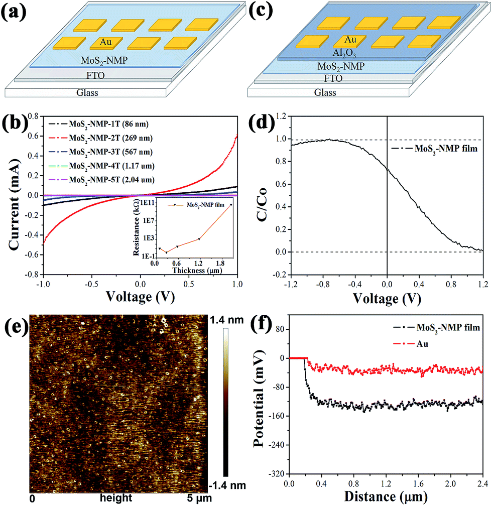 | ||
| Fig. 2 (a) The device structure which was used to measure the conductivity of MoS2-based thin film. (b) The current–voltage curves for MoS2-based thin films with different thicknesses. (c) The device structure which was used to measure high frequency C–V of MoS2-based thin film. (d) High frequency C–V curve of MoS2-based thin films. (e) The AFM height image of MoS2-based thin film. (f) Contact potential line scan profiles of MoS2-based film and Au film measured by AFM. | ||
In order to determine the type of this semiconductor film, a Metal-Oxide-Semiconductor (MOS) device was fabricated in Fig. 2c. MoS2-based thin film was spin-coated twice on FTO-glass substrate. Following this step, 40 nm-thick Al2O3 layer was deposited as dielectric layer by atomic layer deposition (ALD) method. Finally 30 nm-thickness gold was evaporated to complete this MOS structure device, which was used to measure high frequency C–V curve. Fig. 2d shows the high frequency C–V curve. For p-type semiconductor, when bias voltage was positive, semiconductor was in a depletion state. As high frequency signal was applied, the speed of generation and recombination of electron–hole pairs can't come up with that of bias change. So the device capacitance was much small. When bias voltage was negative, holes accumulated on the semiconductor surface. Capacitance C approaches to Co. In contrast, the high frequency C–V curve of n-type semiconductor was opposite to p-type semiconductor. The curve shown in Fig. 2d indicates that MoS2-based thin film obviously exhibits p-type semiconductor characteristic. According to the p + p model proposed by us before,22,23 this p-type film is propitious to act as the back contact of CdTe cells.
Work function is also an important parameter to choose the candidate for the back contact materials of CdTe cells. The work function of MoS2-based thin film was measured by Kelvin probe of atomic force microscopy (KPFM) method (Fig. 2e), and Au film was used as the standard material. The difference of surface potentials (V) between Au and MoS2-based film is about 0.1 V (Fig. 2f). According to the formula below, the work function of MoS2-based film was able to be calculated (about 5.42 eV) due to the known work function of Au (5.32 eV).22,33 Calculation details are presented in the ESI.†
| Φsample − Φtip = −eVCPD |
In summary, MoS2-based film is a p-type semiconductor with a high work function, and a promising candidate for the back contact of CdTe solar cells. Moreover, its fancy thickness-dependent conductivity is positively correlated with the variation tendency of the cell performance.
MoS2-based complex thin film as the back contact in CdTe solar cells
Fig. 3a illustrates a typical procedure of device preparation with MoS2-based thin film as the back contact. A CdS thin film with thickness of about 100 nm was deposited on FTO-glass by magnetron sputtering. Then a CdTe layer with thickness of about 4 μm was prepared by close space sublimation (CSS), following by evaporating a 3 nm-thickness Cu film. Then MoS2-based thin film was prepared by spin-coating and subsequent thermal treatment with different times. Finally the device was completed by evaporating an Au film with thickness of about 30 nm as the back electrode. The SEM images for CdTe cells with/without MoS2-based thin film as the back contact were presented in Fig. S7.† A compact thin film was observed to completely cover the surface of CdTe layer in Fig. S7d.†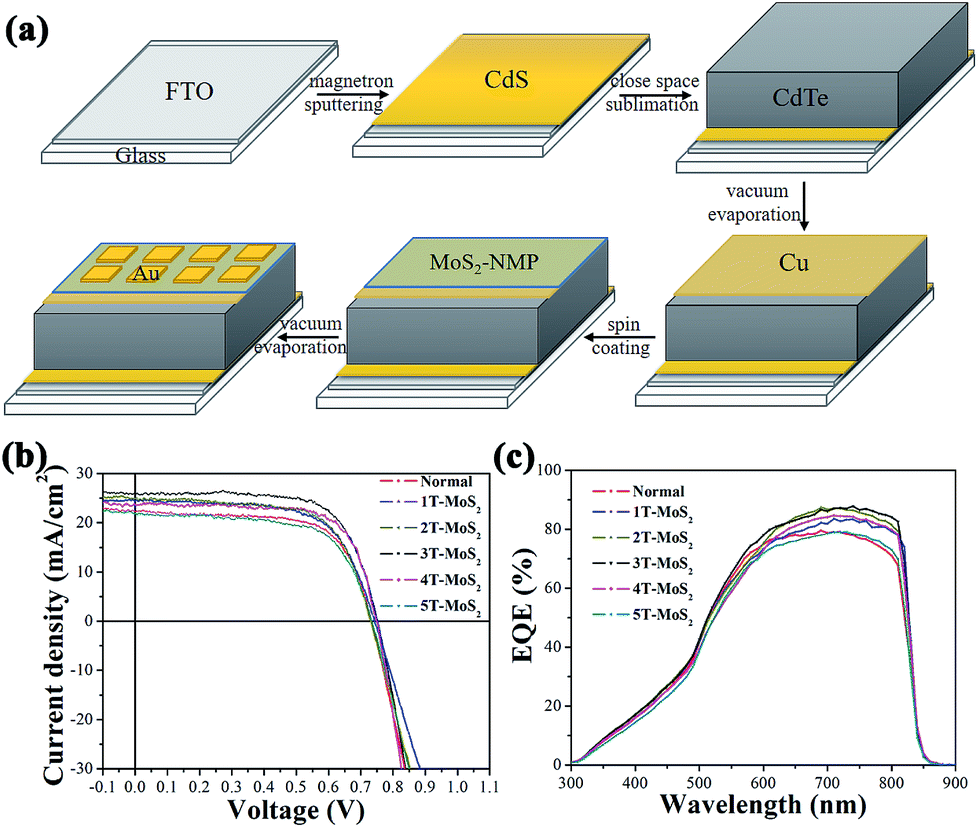 | ||
| Fig. 3 (a) Fabrication procedure of CdTe solar cells. (b) Current density–voltage (J–V) curves of solar cells after spin-coating MoS2–NMP solution zero, once, twice, three, four and five times under AM 1.5 illumination. (c) The EQE spectra of corresponding six solar cells. | ||
At first, we investigated the impact of the thickness of MoS2-based thin film on the efficiency of CdTe solar cells. The traditional CdTe solar cells with the device structure of (FTO/CdS/CdTe/Cu/Au) was used as a reference. According to the different spin-coating times, we finally prepared five cells. 1T-MoS2, 2T-MoS2, 3T-MoS2, 4T-MoS2 and 5T-MoS2 respectively represent the cells with MoS2-based thin film as back contact prepared by spin-coating 1, 2, 3, 4 and 5 times. As shown in Fig. 3b, J–V characteristic curves are recorded for all these cells to evaluate their cell performance.
Obviously, the best efficiency occurred when MoS2–NMP solution was spin-coated three times. With the further increase of spin-coating times, the performance of cells started to degrade. This tendency is consistent with the conductivity of the MoS2-based film. As shown in Fig. 4b. Through the cross-sectional view of the best CdTe cell (3T-MoS2), the thickness of MoS2–NMP film in 3T-MoS2 cell was obtained (about 250 nm). When we previously measured the conductivity of the MoS2–NMP film, MoS2–NMP solution was spin-coated twice, the conductivity of the film is the best. Here, thickness of 2T-MoS2–NMP film is about 269 nm (Fig. 2b). We find that although their spin-coating times are different, their thicknesses are almost the same. It was caused by differences in the substrate (one is CdTe/Cu, the other is FTO). It also explains why the efficiency of 3T-MoS2 cell is the highest. In contrast to the traditional cell, power conversion efficiency was increased from 11.1% to 13.7%. The detailed photovoltaic parameters were listed in Table 1. It is easy to found that the efficiency improvement was mainly from the increasing of short-circuit current (Jsc) from 22.2 to 25.9 mA cm−2. In the meanwhile, fill factor (FF) and open-circuit voltage also gained further optimization (Table 1). According to external quantum efficiency (EQE) spectra (Fig. 3c), we found that the EQE of six cells in range of 300–600 nm were almost the same, obvious difference happened in long-wavelength region (650–850 nm). This hinted that the photogenerated carriers coming from longer-wavelength absorption was effectively transported and collected at the back contact. The increase of EQE in long-wavelength region predicated that MoS2–NMP layer improved the contact interface between CdTe and Au, reduced recombination of electron–hole pairs and enhanced the collection of holes around the back electrode. It indicates that MoS2–NMP layer is a good candidate for the back contact.
 | ||
| Fig. 4 (a) High magnification SEM image of CdTe surface after spin-coating three times. (b) The cross-sectional view of the best CdTe cell (3T-MoS2). (c) The XPS spectra of Mo element with etching depth in CdTe cell (3T-MoS2). (d) The atomic percent of Cd, Te, Cu and Mo with etching depth for CdTe cell (3T-MoS2). (e) The valence spectra of CdTe cell (3T-MoS2) with etching depth. (f) The energy band structure of CdTe solar cells (3T-MoS2). | ||
| No. | Jsca (mA cm−2) | Vocb (V) | FFc | PCEd (%) |
|---|---|---|---|---|
| a Jsc: short-circuit current density.b Voc: open-circuit voltage.c FF: fill factor.d PCE: power conversion efficiency. | ||||
| Normal | 22.2 | 0.733 | 68 | 11.1 |
| 1T-MoS2 | 24.3 | 0.743 | 66 | 11.9 |
| 2T-MoS2 | 25.0 | 0.731 | 66 | 12.1 |
| 3T-MoS2 | 25.9 | 0.752 | 70 | 13.7 |
| 4T-MoS2 | 23.7 | 0.749 | 73 | 12.9 |
| 5T-MoS2 | 22.0 | 0.734 | 66 | 10.6 |
The energy level study for CdTe cells
Fig. 4a shows the morphology of MoS2-based thin film. It presents a flocculent appearance, which is consistent with the amorphous phase determined by XRD above. The sectional view of the best cell, 3T-MoS2, were presented in Fig. 4b. It is clear that the thickness of MoS2-based thin film was not uniform because of the coarse surface of CdTe layer. The mean thickness was estimated as about 250 nm. Mo 3d XPS spectra were recorded in Fig. 4c. Mo 3d peak were basically extinguished below 220 nm, which is consistent with the result of Fig. 4b.To figure out the energy level structure between MoS2-based thin film and CdTe layer, the valence band spectra depth profile were presented in Fig. 4e. The spectra above 200 nm were assigned to MoS2-based thin film. The spectra at 0 nm is not adopted because of the possible pollute from the external environment. The spectra at 110 nm and 220 nm are basically the same. So we regard them as the true spectra for MoS2-based thin film. According to the linear extrapolation method, we could determine the valence maximum (VBM) of MoS2-based thin film as EVBM = 0.15 eV. Then we could find the spectra move to the direction of high binding energy until 660 nm. So we could deduce that the spectra between 220 nm to 660 nm arise from the Cu doped CdTe region, and the region below 660 nm is regarded as the undoped CdTe layer. Similarly, the valence maximum (VBM) of the undoped CdTe layer was derived as EVBM = 0.71 eV. We could also deduce the offset between the valence band positions of CdTe and MoS2-based thin film is 0.56 eV (ΔEVB = 0.56 eV), which is exactly the value of a band bending because of the gradient Cu doping. Using bulk band gaps of 1.45 eV for CdTe and 2.14 eV for MoS2-based thin film, the conduction band offset of ΔEcB = 1.25 eV was deduced by the valence band offset.
According to the corresponding results, combining with the band gaps and work functions of CdTe and MoS2-based thin film, the energy level structure at the interface of CdTe/MoS2-based thin film could be illustrated in Fig. 4f. We could find that there is a good ohmic contact in the interface between CdTe layer and MoS2-based thin layer. Under an electrical field (0.56 eV), the holes in CdTe layer can rapidly be transported to MoS2-based thin layer. Without MoS2-based layer as the back contact, the electrical field intensity in the interface will be decreased from 0.56 eV to 0.46 eV because of the difference (0.1 eV) of work functions between Au film and MoS2-based layer, which weakens its ability to collect holes. Therefore compared with the traditional cell, holes could transport more quickly from CdTe layer to MoS2-based thin film, then to Au film. Meanwhile electrons was blocked to transport from CdTe layer to MoS2-based layer by a large potential barrier (ΔEcB = 1.25 eV), which further reduces the recombination of holes and electrons at the interface. Therefore, we could conclude that the high performance of 3T-MoS2 cell along with the biggest Jsc come from the matchable energy level of CdTe/MoS2-based thin film interface.
Conclusions
In summary, a MoS2-based complex thin film was successfully fabricated by spin-coating. It was constructed by the MoS2(NMP)3 molecules as basic structure unit to stack in a nearly-parallel manner through S⋯H–C hydrogen bonds. It exhibits a very high work function (5.42 eV) with a p-type semiconductor character. More interestingly, a unique thickness-dependent conductivity was found, which might come from the fancy electronic structure of MoS2-based complex thin film with MoS2(NMP)3 molecules as block units. When used it as the back contact of CdTe cells, it produced a high efficiency, which can perform PCE 2.6% higher than that of the traditional cell. The matchable energy level between MoS2-based film and CdTe layer could be responsible for this significant efficiency improvement. This work might open a new direction for the extensive application of two-dimensional transition metal dichalcogenides.Acknowledgements
We thank financial support from the Guangdong Innovative and Entrepreneurial Research Team Program (Grant No. 2013N080), the Peacock Plan (Grant No. KYPT20141016105435850), Shenzhen Key Lab (Grant No. (2012)780 and ZDSY20130331145131323), the International Postdoctoral Exchange Fellowship Program (No. 53 Document of OCPC, 2016).Notes and references
- D. Chen, W. Chen, L. Ma, G. Ji, K. Chang and J. Y. Lee, Mater. Today, 2014, 17, 184–193 CrossRef CAS.
- Y. Jin, D. H. Keum, S. J. An, J. Kim, H. S. Lee and Y. H. Lee, Adv. Mater., 2015, 27, 5534–5540 CrossRef CAS PubMed.
- Y. Xue, Y. Zhang, Y. Liu, H. Liu, J. Song, J. Sophia, J. Liu, Z. Xu, Q. Xu, Z. Wang, J. Zheng, Y. Liu, S. Li and Q. Bao, ACS Nano, 2016, 10, 573–580 CrossRef CAS PubMed.
- M.-Y. Li, Y. Shi, C.-C. Cheng, L.-S. Lu, Y.-C. Lin, H.-L. Tang, M.-L. Tsai, C.-W. Chu, K.-H. Wei, J.-H. He, W.-H. Chang, K. Suenaga and L.-J. Li, Science, 2015, 349, 524–528 CrossRef CAS PubMed.
- D. Jariwala, S. L. Howell, K. S. Chen, J. Kang, V. K. Sangwan, S. A. Filippone, R. Turrisi, T. J. Marks, L. J. Lauhon and M. C. Hersam, Nano Lett., 2016, 16, 497–503 CrossRef CAS PubMed.
- C. H. Lee, G. H. Lee, A. M. van der Zande, W. Chen, Y. Li, M. Han, X. Cui, G. Arefe, C. Nuckolls, T. F. Heinz, J. Guo, J. Hone and P. Kim, Nat. Nanotechnol., 2014, 9, 676–681 CrossRef CAS PubMed.
- M. L. Tsai, S. H. Su, J. K. Chang, D. S. Tsai, C. H. Chen, C. I. Wu, L. J. Li, L. J. Chen and J. H. He, ACS Nano, 2014, 8, 8317–8322 CrossRef CAS PubMed.
- Z. Yin, X. Zhang, Y. Cai, J. Chen, J. I. Wong, Y. Y. Tay, J. Chai, J. Wu, Z. Zeng, B. Zheng, H. Y. Yang and H. Zhang, Angew. Chem., Int. Ed., 2014, 53, 12560–12565 CAS.
- K. Chang, M. Li, T. Wang, S. Ouyang, P. Li, L. Liu and J. Ye, Adv. Energy Mater., 2015, 5, 1402279 CrossRef.
- J. Zhang, S. Najmaei, H. Lin and J. Lou, Nanoscale, 2014, 6, 5279–5283 RSC.
- T. Du, N. Wang, H. Chen, H. He, H. Lin and K. Liu, J. Power Sources, 2015, 275, 943–949 CrossRef CAS.
- K. Kalantar-zadeh, J. Z. Ou, T. Daeneke, M. S. Strano, M. Pumera and S. L. Gras, Adv. Funct. Mater., 2015, 25, 5086–5099 CrossRef CAS.
- Y. Zang, J. Lei, Q. Hao and H. Ju, Biosens. Bioelectron., 2016, 77, 557–564 CrossRef CAS PubMed.
- K. F. Mak, C. Lee, J. Hone, J. Shan and T. F. Heinz, Phys. Rev. Lett., 2010, 105, 136805 CrossRef PubMed.
- S. G. Kumar and K. S. R. K. Rao, Energy Environ. Sci., 2014, 7, 45–102 CAS.
- A. N. Tiwari, G. Khrypunov, F. Kurdzesau, D. L. Bätzner, A. Romeo and H. Zogg, Prog. Photovoltaics, 2004, 12, 33–38 CAS.
- K. Shen, R. Yang, D. Wang, M. Jeng, S. Chaudhary, K. Ho and D. Wang, Sol. Energy Mater. Sol. Cells, 2016, 144, 500–508 CrossRef CAS.
- H. Dang and V. P. Singh, Sci. Rep., 2015, 5, 14859 CrossRef CAS PubMed.
- R. Yang, D. Wang, M. Jeng, K. Ho and D. Wang, Prog. Photovoltaics, 2016, 24, 59–65 CAS.
- S. Hu, Z. Zhu, W. Li, L. Feng, J. Zhang, L. Wu and B. Li, Sol. Energy Mater. Sol. Cells, 2015, 134, 329–333 CrossRef CAS.
- B. Siepchen, B. Späth, C. Drost, V. Krishnakumar, C. Kraft, M. Winkler, J. König, K. Bartholomé and S. Peng, J. Electron. Mater., 2015, 44, 3354–3359 CrossRef CAS.
- M. J. Zhang, Q. X. Lin, X. Y. Yang, Z. W. Mei, J. Liang, Y. Lin and F. Pan, Nano Lett., 2016, 16, 1218–1223 CrossRef CAS PubMed.
- J. Liang, Q. X. Lin, H. Li, Y. T. Su, X. Y. Yang, Z. Z. Wu, J. X. Zheng, X. W. Wang, Y. Lin and F. Pan, Appl. Phys. Lett., 2015, 107, 013907 CrossRef.
- Q. Lin, Y. Su, M. J. Zhang, X. Yang, S. Yuan, J. Hu, Y. Lin, J. Liang and F. Pan, Chem. Commun., 2016, 52, 10708–10711 RSC.
- D. Gopalakrishnan, D. Damien and M. M. Shaijumon, ACS Nano, 2014, 8, 5297–5303 CrossRef CAS PubMed.
- W. K. Metzger, D. Albin, M. J. Romero, P. Dippo and M. Young, J. Appl. Phys., 2006, 99, 103703 CrossRef.
- L. Zhang, J. L. Da Silva, J. Li, Y. Yan, T. A. Gessert and S. H. Wei, Phys. Rev. Lett., 2008, 101, 155501 CrossRef PubMed.
- B. E. McCandless, L. V. Moulton and R. W. Birkmire, Prog. Photovoltaics, 1997, 5, 249–260 CAS.
- M. J. Zhang, X. M. Jiang, L. J. Zhou and G. C. Guo, J. Mater. Chem. C, 2013, 1, 4754–4760 RSC.
- C. Z. Wang, L. P. Han, P. J. Chen, G. F. Zhao, Y. Liu and Y. Lu, J. Catal., 2016, 337, 145–156 CrossRef CAS.
- B. Auer, R. Kumar, J. R. Schmidt and J. L. Skinner, Proc. Natl. Acad. Sci. U. S. A., 2007, 104, 14215–14220 CrossRef CAS PubMed.
- T. Fornaro, D. Burini, M. Biczysko and V. Barone, J. Phys. Chem. A, 2015, 119, 4224–4236 CrossRef CAS PubMed.
- V. De Renzi, R. Rousseau, D. Marchetto, R. Biagi, S. Scandolo and U. Del Pennino, Phys. Rev. Lett., 2005, 95, 046804 CrossRef CAS PubMed.
Footnote |
| † Electronic supplementary information (ESI) available. See DOI: 10.1039/c7ra03233a |
| This journal is © The Royal Society of Chemistry 2017 |