
 Open Access Article
 This Open Access Article is licensed under a Creative Commons Attribution-Non Commercial 3.0 Unported Licence
A high-performance TiO2 nanowire UV detector assembled by electrospinning
Yuting Wang ,
Jing Cheng,
Muhammad Shahid,
Mengfei Zhang and
Wei Pan*
,
Jing Cheng,
Muhammad Shahid,
Mengfei Zhang and
Wei Pan*
State Key Laboratory of New Ceramic and Fine Processing, School of Materials Science and Engineering, Tsinghua University, Beijing 100084, P. R. China. E-mail: panw@mail.tsinghua.edu.cn; Fax: +86-10-62771160; Tel: +86-10-62772858
First published on 16th May 2017
Abstract
Here, a transparent, flexible and nanoscale TiO2 ultraviolet (UV) photodetector has been fabricated by electrospinning. Well aligned TiO2 nanowires were collected on a flexible mica substrate. Then, the nano-device was simply assembled by depositing interdigitated platinum electrodes on the surface. Upon UV illumination, the photosensitivity of this device is up to over three orders of magnitude with relatively fast and stable response speed under 254 nm and 365 nm UV light. This nanosensor retains a high photo-dark current ratio, fast response time and stable durability during bending tests, indicating an excellent reversibility and stability of the flexible TiO2 nanowires. The highly flexible photosensor demonstrates a good potential candidate for wearable optoelectronic applications.
1. Introduction
Flexible or stretchable electronic devices with high mechanical stability are considered key components for next generation wearable smart electronics.1–3 Although inorganic-based semiconducting nanomaterials present excellent UV sensitivity and fast response/recovery speed,4 the poor flexibility of ceramic materials hinders their wide application.5 Flexible photodetectors based on bendable plastic substrates have attracted great attention because of their potential applications in optoelectronics, sensors, and transducers, etc.3,6,7 Among various ceramic oxides, titanium dioxide, as an n-type semiconductor with a wide bandgap (anatase 3.2 eV and rutile 3.0 eV), is well known for its versatile characteristics in photocatalysis, solar cells, and diodes etc.8–11 In particular, TiO2 has been widely used in photocatalysis because of its outstanding photocatalytic activity and electronic properties.12–17 Many nanotechniques have been developed to fabricate one-dimensional (1D) TiO2, such as nanorods,18 nanowires,19 nanobelts,20 and nanotubes.21 Three crystal phases of TiO2 are well known as rutile, anatase, and brookite.22 Although the bandgap energy for anatase phase (∼3.2 eV) is larger than the rutile (∼3 eV), it shows high photocatalytic activity and efficiency of the charge carrier photogeneration when combining anatase and rutile mixtures of TiO2 nanocrystalline with a radio of 80% and 20%.23,24 As we known, few research has reported about the photoresponse performance of TiO2-based photodetector.Electrospinning is a facile approach to produce one-dimensional (1D) nanostructures with great scalability. The diameter and morphology of the electrospun nanofibers could be simply controlled by adjusting the density of precursor solutions, applied voltage, working distance and spinning rate.25 Moreover, this nanomaterial synthesize technology shows advantages of low cost, high efficiency and convenient assembly. Electrospun nanofibers demonstrate outstanding electric, optic, mechanical and magnetic flexibility properties, with considerable potential for novel applications in different fields.26–29 However, most of the reports for electrospun nanofibers concentrated on the 1D nanostructures. More detailed research on the fabrication of two-dimensional (2D) networks has not been reported so much. Actually, the collected eletrospun nanowires could be automatically formed as a nanoweb on the plate substrate. Therefore, in this study, electrospinning was used for fabricating ultralong nanowires and flexible 2D nanowebs by simply annealing these 2D networks in air.
Here, we report a high-performance 2D nanoweb photosensor composed of ultralong 1D-structured TiO2 nanowires. The nanoweb-based photodetector shows high photo-dark current ratio, excellent mechanical flexibility and durability. Possible mechanisms of the improved mechanical performance of this TiO2 nanosensor have been discussed in detail.
2. Experimental section
TiO2 nanowires were synthesized using an electrospinning approach. Tetrabutyl titanate (6 wt% of the ceramic precursor) was first dissolved in the mixture of ethanol–acetic acid (3.3![[thin space (1/6-em)]](https://www.rsc.org/images/entities/char_2009.gif) :1, volume rate). After stirring for 30 min, a concentration of 6 wt% polyvinylpyrrolidone (PVP, MW = 1300000) was further mixed to control the viscosity. Afterward, the prepared solution was stirred at room temperature for 2 h to achieve complete dissolution and mixing. After dissolution of all the components, the obtained transparent precursor solution was placed in a hypodermic syringe at the positive voltage of 15 kV with a constant flow rate of 0.5 mL h−1. The distance between the needle tip and the aluminum foil collector was 15 cm. Finally, nanofiber webs were removed from the collector and annealed in air at different temperatures, 550 °C, 600 °C, 700 °C, and 800 °C for 1 h with the heating rate of 5 °C min−1, respectively.
:1, volume rate). After stirring for 30 min, a concentration of 6 wt% polyvinylpyrrolidone (PVP, MW = 1300000) was further mixed to control the viscosity. Afterward, the prepared solution was stirred at room temperature for 2 h to achieve complete dissolution and mixing. After dissolution of all the components, the obtained transparent precursor solution was placed in a hypodermic syringe at the positive voltage of 15 kV with a constant flow rate of 0.5 mL h−1. The distance between the needle tip and the aluminum foil collector was 15 cm. Finally, nanofiber webs were removed from the collector and annealed in air at different temperatures, 550 °C, 600 °C, 700 °C, and 800 °C for 1 h with the heating rate of 5 °C min−1, respectively.
The morphologies of TiO2 nanowires and flexible nanowebs were observed by scanning electron microscopy (SEM, JEOL JSM-6460LV, Tokyo, Japan) and transmission electron microscopy (TEM, JEOL-2011, Tokyo, Japan). A diffractometer (XRD, D/max-2500, Rigaku Co., Tokyo, Japan) was used to examine the crystal structures of these samples. The current–voltage (I–V) characteristics of TiO2 networks were measured by a Keithley (4200 system, Cleveland, OH, USA). Moreover, the photoresponse characteristics of the UV detectors were monitored using UV light (Philips TUV 8 W, 254 nm, an average power density of 0.5 W cm−2).
3. Result and discussion
Intuitively, the flexible photosensor consists of semi-conductive nanowires and platinum electrodes, shown in Fig. 1a. By electrospinning, continuous aliened TiO2 nanowires are first collected on a flexible and transparent mica substrate. Pt electrodes were deposited using a mask by high quality vacuum evaporation. Fig. 1b shows a photograph of the flexible sensor attached to a nonplanar surface. The morphology and microstructures of highly oriented TiO2 nanowires were observed by SEM (Fig. 1c and d). Ultra-long TiO2 nanowires preserve their continuity after 1 h annealing under air. Magnified image shows smooth surfaces and a uniform diameter of ∼200 nm of the nanowires. The smooth surface and continues structure of these nanowires reveal that they would have more uniform strength and thus more easily to release the strain compared with fibers of rough surfaces and short lengths upon bending. The TEM image in Fig. 1e also shows a fibrillar structure and a smooth surface of the annealed TiO2 nanowire. A selected-area electron diffraction (SAED) pattern shown in the inset of Fig. 1e reveals that the nanofibers are comprised of polycrystalline and fine grains with no preferential orientation. Fig. 1f shows a high-resolution transmission electron microscopy (HRTEM) image with distances of crystal lattice fringes of 3.5 Å that can be attributed to the spacing of (101) lattice plane of the anatase TiO2.30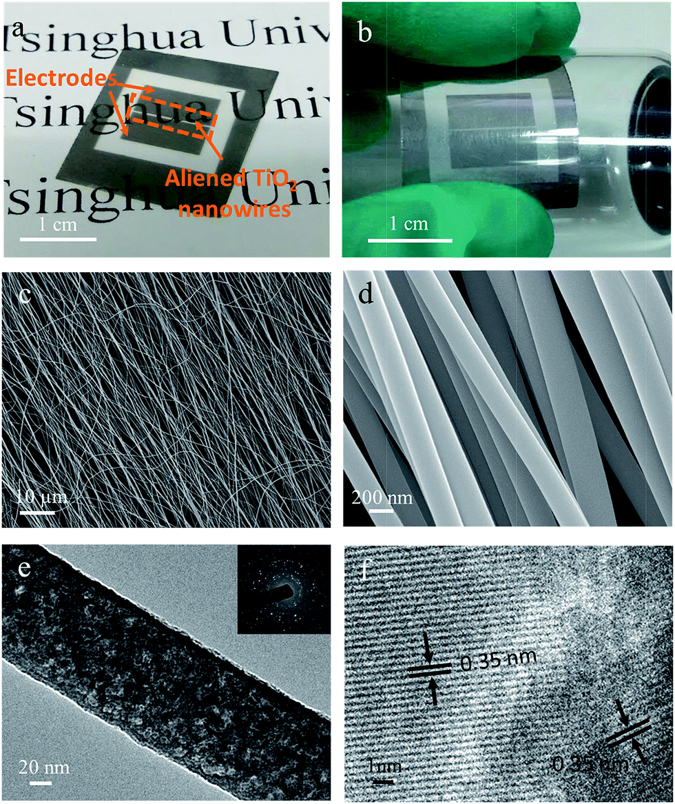 | ||
| Fig. 1 Highly oriented TiO2 nanowire photosensor. (a) Schematic representation of the device assembled by aliened TiO2 array and coated Pt electrodes. (b) Photograph of the photosensor attached to curved surface. (c and d) SEM images of highly oriented TiO2 nanowires. (e and f) TEM and HRTEM images of the TiO2 nanowire annealed to 550 °C. The inset shows the SAED pattern. | ||
Ultra-long TiO2 nanowires can be further assembled to a two-dimensional nanopaper. This free-standing nanopaper could be bended without any cracking. SEM measurements were used to determine the strength of TiO2 nanoweb. Fig. 2a and b show the distinct boundary of the folded nanopaper. The TiO2 nanofibers are not broken or got any fracture when bended in half. Moreover, spring- and wave-like structures have been spontaneous formed during eletrospinning.31 After annealing, the spring-like nanowires could maintain their curly and wavy geometries, attributing to the superior mechanical flexibility of TiO2 nanomaterials. Fig. 2d shows that the freestanding TiO2 networks are successfully folded in half and remain intact. The mechanistic explanation is that the TiO2 nanowires remain continuous and undergo nano-scaled deformation to relax the applied stress upon folding.
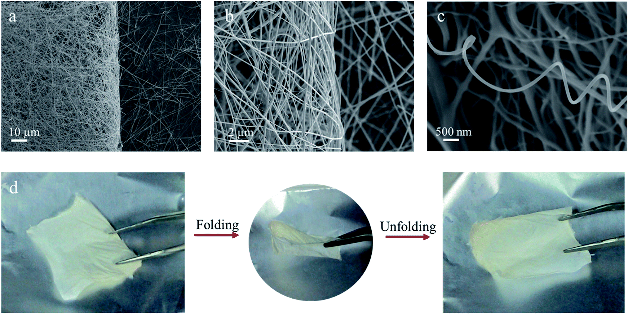 | ||
| Fig. 2 Flexible TiO2-based ceramic nanopapers. (a and b) SEM images of the flexible nanopaper folded in half. (c) SEM image of a spring-like TiO2 nanowire. (d) Photographs of TiO2 network-based ceramic nanopaper under folding and unfolding. | ||
To investigate the crystal structure of the nanofibers, X-ray diffraction (XRD) analyses of TiO2 nanofiber-based powders were observed after annealing at 500 °C, 550 °C, 600 °C, 700 °C, and 800 °C for 1 h in Fig. 3. The as-spun nanofibers are amorphous in nature, and the polycrystalline nanofibers are formed after calcination at 500 °C. We note that the annealing temperature could distinctly affect the phase compositions of the TiO2 nanowires. As the sample is calcined at 500 °C, a phase occurs with a low and wide characteristic peak corresponding to the typical anatase crystal, and this phase completely disappears at 800 °C, leaving pure rutile phases. The XRD patterns also show a mixture of anatase and rutile phases in the annealing range of 500 to 700 °C. It proves that the different ratio of these two phases in TiO2 composite could be simply controlled by annealing at different temperatures. Contrasting the strength of the anatase (101) peak and the rutile (110) peak in Fig. 3, the concentration of anatase phase in hybrid TiO2 nanofibers can be estimated as 92%, 83%, 75%, 17%, and 6%, corresponding to the annealing temperature change from 500 to 800 °C, respectively. It was reported that anatase TiO2 shows more photocatalytic activity than its rutile phase due to its large surface area,24,32 thus, in this study, the high-performance TiO2 nanosensor is composed of a majority of anatase phases combined with little amount of rutile phases. With the high reactivity of anatase TiO2 together with the lower band gap of rutile TiO2, the process of the photoinduced electrons and holes transfer between conduction and valence bands can be highly facilitated in the composite sample.
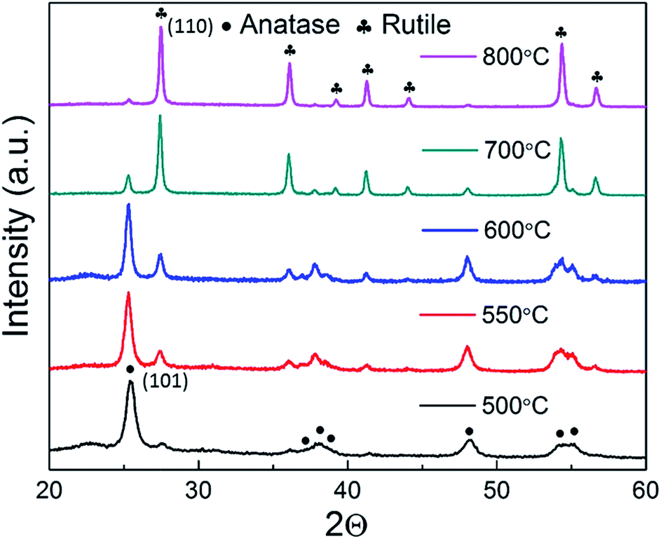 | ||
| Fig. 3 XRD patterns of a TiO2 nanowires annealed at different temperatures. | ||
The mechanism of phase-dependent photoresponse activity in phase junction TiO2 nanowires is drawn in Fig. 4a. The band gaps of anatase and rutile phases of TiO2 are 3.2 and 3.0 eV, respectively. This means that when the two phases are in nano-contact there will be a phase junction between the band edges. The phase junctions can promote charges transfer from anatase to rutile phases, similar to the mechanism of P25.24,33 When the photosensor is illuminated under UV light with photon energy higher than the band gap of anatase TiO2, electrons in the valence band can be excited to the conductive band with the generation of the same amount of holes. Generally these electron–hole pairs are easily recombined that reducing the photoresponse of semiconductors. However, the existing two phases make it possible for the photogenerated charges to migrate from anatase to rutile phases and to efficiently separate the photoinduced electron–hole pairs.
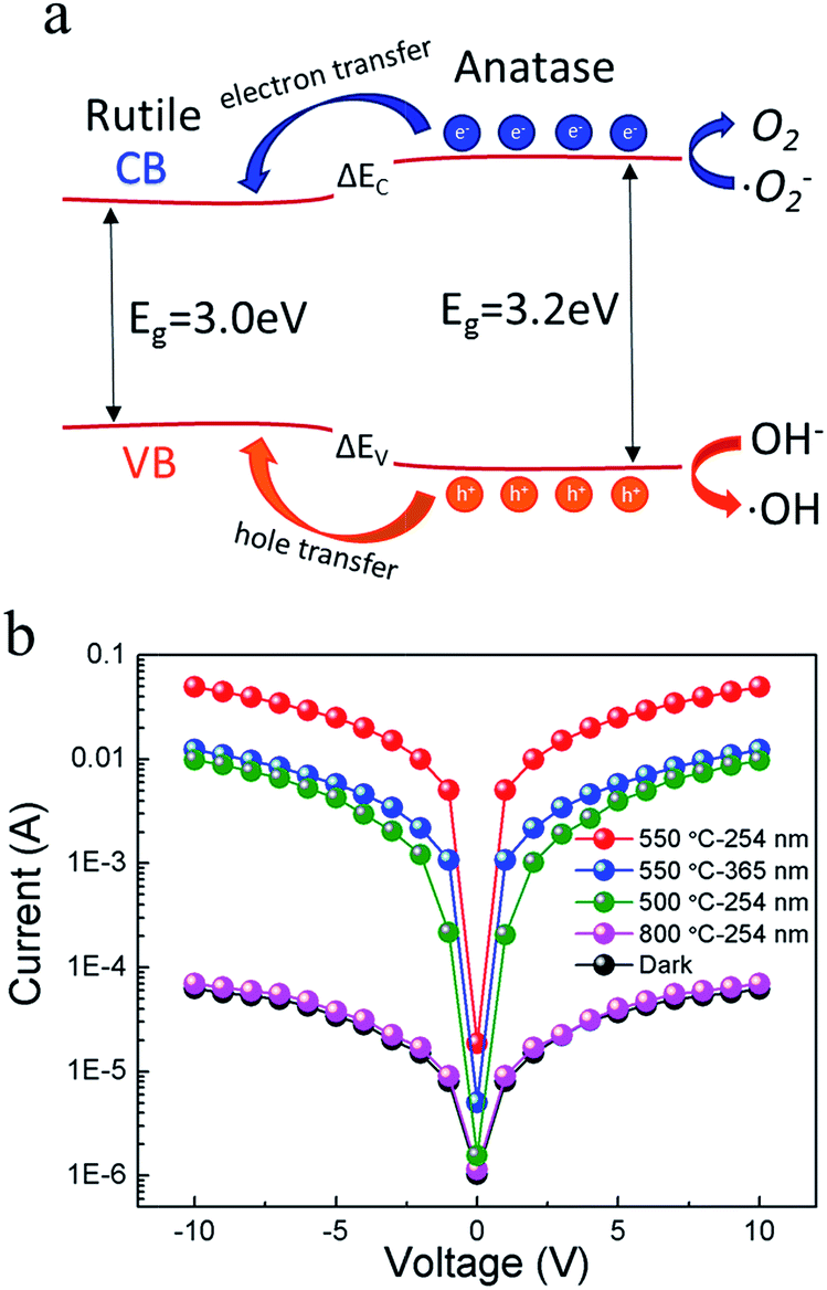 | ||
| Fig. 4 (a) Schematic illustration of the band structure related mechanism for the anatase/rutile TiO2 phase junction. (b) I–V curves of the flexible TiO2 photodetector calcined at 500, 550 and 800 °C under dark or different light illuminations; the incident light power density = 500 μW cm−2. | ||
The developed single TiO2 nanowire shows a low dark current of approximately pA level even at an applied voltage of 10 V, as shown in Fig. 4b. A significant increase in the current is observed under 254 nm UV light illumination (500 μW cm−2) with a high photocurrent-to-dark current ratio of at approximately three orders of magnitude. The photocurrent of the sample annealed at 550 °C could reach up to 47 nA and 38 nA under 254 nm and 365 nm UV light at an applied voltage of 10 V, corresponding to a photo-dark current ratio of 760 and 600, respectively. For comparison, the photo-dark current ratio of the anatase (annealed at 500 °C) and rutile (annealed at 800 °C) TiO2 nanowires are 160 and 1.1, respectively. The performance of the composite TiO2 nanowires is comparable with other reported ZnO-based and TiO2-based photodetectors.34–38 Compared with reported flexible ZnO nanowires,39,40 our TiO2 network photosensor shows much better flexibility. For the ZnO photosensors, they can withstand a bending radius of 10 mm or 15 mm. But the photosensor would keep stable only after releasing the strain. In our case, the photoresponse tests were measured while the sensor was under bending.
The flexibility of TiO2 photodetector annealed at 550 °C was studied by bending to different curvature radii and repeated bending tests. It is noteworthy that the I–V characteristics keep linear and remain stable under UV light illumination, as shown in Fig. 5a. When bended to a radius from 100 to 5 mm, the responsivity shows a little decrease upon illumination at 254 nm. Even at the smallest curvature radius of 5 mm, the responsivity shows a high retention of 85% and 65% at 10 V and 1 V, respectively (Fig. 5c). The retention of responsivities at curvature radius of 100 mm and 10 mm was tested to be 96% and 78% during cycling under bending (Fig. 4b), respectively. This excellent flexible performance could be corresponding to the SEM results and visible bending tests in Fig. 2. As the TiO2 nanowire could retain a continues nanostructure without any cracking, the electrical properties of them could also keep stable under bending. The response time of photodetector is another major issue for its practical application. Fig. 5d shows the response time of photodetector upon 254 nm illumination at 1 V and 10 V. When the applied voltage is 1 V, this response time decreases slightly under bending. With a higher voltage of 10 V excites the photosensor, this photoresponse time could be remained stable even after bending to a curvature radium of 5 mm. These results demonstrate the great mechanical flexibility and durability of this TiO2 photodetector.
 | ||
| Fig. 5 (a) I–V curves of the flexible TiO2 nanopaper photodetector annealed at 550 °C under dark or UV light illumination. (b) Photo-switching characteristics of the photosensor under dark and UV light. Plot of sensitivity (c) or response time (d) versus bending curvature radium of the photosensor under 254 nm at 1 or 10 V bias. | ||
To confirm the band gap of TiO2 nanowires, Fig. 6a shows UV-vis diffuse reflection spectra of the TiO2 nanowires annealed at 550 °C. The direct band gap of TiO2 nanowires can be estimated by UV-vis diffuse reflection spectra using the following formation:41(αhν)2 = A(hν − Eg)where α is the absorption coefficient, h is Planck's constant, ν is the photon frequency, A, a constant, and Eg is the optical band gap, respectively. Therefore, the band gap of the TiO2 nanowires can be estimated from the data shown in Fig. 6b, corresponding to the energy band gap about 3.15 eV. This value is below that of anatase but higher than rutile TiO2 shown in Fig. 4a, suggesting that the TiO2 sample calcined at 550 °C consists of both anatase and rutile phases, corresponding to the XRD results.
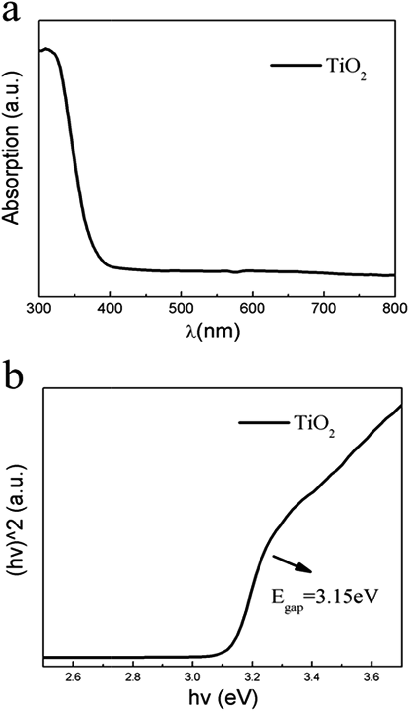 | ||
| Fig. 6 (a) UV-visible diffuse reflection spectra of TiO2 nanowires calcined at 550 °C, and (b) the corresponding plots of (αhν)2 versus photon energy (hν). | ||
4. Conclusions
In summary, a highly flexible TiO2 photosensor was successfully fabricated via a facile electrospinning method. Not only did this photosensor show a high photo-dark current ratio of 760 and 600 under 254 nm and 365 nm UV light, respectively, but also exhibit excellent mechanical flexibility and durability. The possible mechanism is that the TiO2 nanowires remain continuous and undergo nano-scaled deformation to relax the applied stress upon bending. Further observations under XRD demonstrate that the crystal structure of this sensor is composed of approximately 83% anatase and 17% rutile phases. The energy band gap of TiO2 nanowebs is calculated to be 3.15 eV, which is a little lower than that of anatase but higher than rutile phase, corresponding to the XRD results. Both of these results could be correlated to the efficient electron–hole transfer between the two phases in the composites, which lead to the superior UV responsibility of our photosensor.Acknowledgements
This study was supported financially by the Natural Science Foundation of China (Grant No. 51323001).References
- M. Y. Lee, J. Hong, E. K. Lee, H. Yu and H. Kim, Adv. Funct. Mater., 2016, 26, 1445 CrossRef CAS.
- X. Wang and G. Shi, Energy Environ. Sci., 2015, 8, 79 Search PubMed.
- N. Liu, H. Tian, G. Schwartz, J. B. H. Tok, T. Ren and Z. Bao, Nano Lett., 2014, 14, 3702 CrossRef CAS PubMed.
- Z. Alaie, S. M. Nejad and M. H. Yousefi, Mater. Sci. Semicond. Process., 2015, 29, 16 CrossRef CAS.
- H. Wu, W. Pan, D. Lin and H. Li, J. Adv. Ceram., 2012, 1, 2 CrossRef CAS.
- C. S. Boland, U. Khan, G. Ryan, S. Barwich, R. Charifou, A. Harvey, C. Backes, Z. Li, M. S. Ferreira, M. E. Mobius, R. J. Young and J. N. Coleman, Science, 2016, 354, 1257 CrossRef CAS PubMed.
- W. Tian, C. Zhang, T. Zhai, S. L. Li, X. Wang, M. Liao, K. Tsukagoshi, D. Golberg and Y. Bando, Chem. Commun., 2013, 49, 3739 RSC.
- H. Xue, W. Chen, C. Liu, X. Kong, P. Qu, Z. Liu, J. Zhou and L. Shen, 3rd IEEE International Conference on Nano/Micro Engineered and Molecular Systems, 2008, 1, 108 Search PubMed.
- Y. Chiba, A. Islam, R. Komiya, N. Koide and L. Han, Appl. Phys. Lett., 2006, 88, 223503 CrossRef.
- C. Wu, C. Chao and F. Kuo, Catal. Today, 2004, 97, 103 CrossRef CAS.
- R. Asahi, T. Morikawa, T. Ohwaki, K. Aoki and Y. Taga, Science, 2001, 293, 269 CrossRef CAS PubMed.
- R. Daghrir, P. Drogui and D. Robert, Ind. Eng. Chem. Res., 2013, 52, 3581 CrossRef CAS.
- G. Jeong, J. Kim, M. Park, M. Seo, S. M. Hwang, Y. Kim, Y. Kim, J. H. Kim and S. X. Dou, ACS Nano, 2014, 8, 2977 CrossRef CAS PubMed.
- Z. Sun, J. H. Kim, T. Liao, Y. Zhao, F. Bijarbooneh, V. Malgras and S. X. Dou, CrystEngComm, 2012, 14, 5472 RSC.
- F. H. Bijarbooneh, Y. Zhao, Z. Sun, Y. Heo, V. Malgras, J. H. Kim and S. X. Dou, APL Mater., 2013, 1, 32106 CrossRef.
- J. Kim, D. Shi, K. Kong, Y. Heo, J. H. Kim, M. R. Jo, Y. C. Lee, Y. Kang and S. X. Dou, ACS Appl. Mater. Interfaces, 2013, 5, 691 CAS.
- J. Na, J. Kim, C. Park and E. Kim, RSC Adv., 2014, 4, 44555 RSC.
- R. S. Chen, C. A. Chen, H. Y. Tsai, W. C. Wang and Y. S. Huang, Appl. Phys. Lett., 2012, 100, 123108 CrossRef.
- L. Lin, L. Liu, K. Musselman, G. Zou and W. W. Duley, Adv. Funct. Mater., 2016, 33, 5979 CrossRef.
- Z. Zhao, J. Tian, Y. Sang, A. Cabot and H. Liu, Adv. Mater., 2015, 27, 2557 CrossRef CAS PubMed.
- J. Zou, Q. Zhang, K. Huang and N. Marzari, J. Phys. Chem. C, 2010, 114, 10725 CAS.
- A. Pottier, C. Chaneac, E. Tronc, L. Mazerolles and J. Jolivet, J. Mater. Chem., 2001, 11, 1116 RSC.
- S. Bakardjieva, J. Subrt, V. Stengl, M. J. Dianez and M. J. Sayagues, Appl. Catal., B, 2005, 58, 193 CrossRef CAS.
- R. I. Bickley, T. Gonzalez-Carreno, J. S. Lees, L. Palmisano and R. J. D. Tilley, J. Solid State Chem., 1991, 92, 178 CrossRef CAS.
- A. Baji, Y. Mai, S. Wong, M. Abtahi and P. Chen, Compos. Sci. Technol., 2010, 70, 703 CrossRef CAS.
- H. Wu, D. Kong, Z. Ruan, P. Hsu, S. Wang, Z. Yu, T. J. Carney, L. Hu, S. Fan and Y. Cui, Nat. Nanotechnol., 2013, 8, 421 CrossRef CAS PubMed.
- C. Niu, J. Meng, X. Wang, C. Han, M. Yan, K. Zhao and X. Xu, Nat. Commun., 2015, 6, 1 Search PubMed.
- L. Zhu, X. Gu, F. Qu, J. Zhang and C. Feng, J. Am. Ceram. Soc., 2013, 96, 3183 CAS.
- J. Cheng, H. Li, S. Huang and W. Pan, J. Am. Ceram. Soc., 2014, 8, 2372 CrossRef.
- J. Cheng, Y. Wang, Y. Xing, M. Shahid and W. Pan, RSC Adv., 2017, 7, 15330 RSC.
- W. E. Teo and S. Ramakrishna, Nanotechnology, 2006, 17, 89 CrossRef PubMed.
- D. Yang, H. Liu, Z. Zheng, Y. Yuan, J. Zhao and E. R. Waclawik, J. Am. Chem. Soc., 2009, 131, 17885 CrossRef CAS PubMed.
- T. Kawahara, Y. Konishi, H. Tada, N. Tohge, J. Nishii and S. Ito, Angew. Chem., 2002, 114, 2935 CrossRef.
- C. Soci, A. Zhang, B. Xiang, S. A. Dayeh, D. P. R. Aplin, J. Park, X. Y. Bao, Y. H. Lo and D. Wang, Nano Lett., 2007, 7, 1003 CrossRef CAS PubMed.
- C. Lu, S. Chang, S. Chang, C. Lee and C. Kuo, Appl. Phys. Lett., 2006, 89, 153101 CrossRef.
- G. Liu, N. Hoivik and K. Wang, Electrochem. Commun., 2013, 28, 107 CrossRef CAS.
- T. Tsai, S. Chang, W. Weng, C. Hsu, S. Wang, C. Chiu, T. Hsueh and S. Chang, J. Electrochem. Soc., 2012, 159, J132 CrossRef CAS.
- W. Zheng, X. Li, G. He, X. Yan, R. Zhao and C. Dong, RSC Adv., 2014, 4, 21340 RSC.
- Z. Zheng, L. Gan, H. Li, Y. Ma, Y. Bando, D. Golberg and T. Zhai, Adv. Funct. Mater., 2015, 25, 5885 CrossRef CAS.
- Y. Wang, M. Shahid, J. Cheng, H. Nishijima and W. Pan, Nanotechnology, 2017, 28, 155202 CrossRef PubMed.
- P. Singh, A. Kumar, A. Kaushal, D. Kaur, A. Pandey and R. N. Goyal, Bull. Mater. Sci., 2008, 31, 573 CrossRef CAS.
| This journal is © The Royal Society of Chemistry 2017 |