
 Open Access Article
 This Open Access Article is licensed under a Creative Commons Attribution-Non Commercial 3.0 Unported Licence
Controllable synthesis and magnetotransport properties of Cd3As2 Dirac semimetal nanostructures†
Kang Zhang‡
a,
Haiyang Pan‡b,
Minhao Zhanga,
Zhongxia Weib,
Ming Gaoa,
Fengqi Song*b,
Xuefeng Wang *a and
Rong Zhanga
*a and
Rong Zhanga
aNational Laboratory of Solid State Microstructures, Collaborative Innovation Center of Advanced Microstructures, School of Electronic Science and Engineering, Nanjing University, Nanjing, Jiangsu 210093, P. R. China. E-mail: xfwang@nju.edu.cn
bNational Laboratory of Solid State Microstructures, Collaborative Innovation Center of Advanced Microstructures, College of Physics, Nanjing University, Nanjing, Jiangsu 210093, P. R. China. E-mail: songfengqi@nju.edu.cn
First published on 22nd March 2017
Abstract
Cd3As2, known as the three-dimensional (3D) analogue of graphene, is a Dirac semimetal with a linear dispersion relation along all three directions in momentum space. Here, Cd3As2 nanostructures with various morphologies, including nanowires, nanobelts, nanoplates and nano-octahedra, were synthesized by a facile chemical vapour deposition method. All these kinds of morphologies can be synthesised by carefully adjusting the pressure and argon flow rate. Further, we systematically investigated the magnetotransport properties of the as-grown nanostructures. The temperature dependences of resistance all displayed insulating behaviour, indicating the low carrier density and the Fermi level close to the Dirac point in our Cd3As2 nanostructures. All nanodevices hosted the unsaturated magnetoresistance even up to 14 T. The linear magnetoresistance was observed in nanodevices based on nanoribbons and nanowires. Our detailed study on the morphology regulation and magnetotransport properties of Cd3As2 nanostructures is valuable for the understanding of the growth process and the future nanoelectronic applications of 3D Dirac semimetals.
Introduction
Recently, the three-dimensional (3D) Dirac semimetal has attracted lots of attention due to its special band structure in which the conduction and valence bands contact only at discrete points in the Brillouin Zone (BZ) and disperse linearly in all directions around these critical points.1–6 When the time-reversal symmetry is broken, the Dirac point in the Dirac semimetal can be evolved into two separate degenerate Weyl nodes with opposite chirality.2,7 Cd3As2, predicted to be a kind of 3D Dirac semimetal,2 was soon verified by angle-resolved photoemission spectroscopy (ARPES) experiments with a pair of Dirac points in the vicinity of the Γ point along kz.8,9 Owing to the unusual energy band property, many novel quantum transport phenomena, such as quantum oscillations,10–16 ultrahigh mobility,8,10,15 superconductivity phase17–19 and large magnetoresistance13,15,20 have been observed in bulk Cd3As2 single crystals. The band structure of Cd3As2 can be engineered by transition metal doping to realize a semiconductor, metal, or half-metal.21 However, the bulk Cd3As2 materials exhibit high carrier density (4.4 × 10¹⁸ to 1.5 × 1019 cm−3), resulting in the Fermi level away from the Dirac point.15 The carrier density of Cd3As2 materials can be suppressed effectively when the sample dimension decreases.22 Even the band gap can be opened in the thin nanowires.2,22 Novel phenomena emerged in Cd3As2 nanostructures, including the negative magnetoresistance,23,24 the quantum oscillations,22,25 linear magnetoresistance,24 Aharonov–Bohm (AB) oscillation26 and semiconductor-like ambipolar effect22 have been observed in Cd3As2 nanostructures. Chemical vapour deposition (CVD) is the most prominent method to synthesize Cd3As2 nanostructures. Recently, Zhang et al.22 reported the vapour–solid (VS) growth of Cd3As2 nanowires without any catalytic sources, and in the meanwhile, the Au-catalytic vapour–liquid–solid (VLS) growth of Cd3As2 nanowires was reported by Wang et al.26 and Li et al.23 Thus Cd3As2 nanostructures grown by CVD method offer an excellent alternative system to study the intriguing property of Dirac semimetal.In this work, by using a particular CVD method, we have synthesized various Cd3As2 nanostructures with different morphologies, including nanowires, nanobelts and microcrystals with regular morphologies. More importantly, the morphologies of Cd3As2 nanostructures can be controlled effectively by adjusting the pressure in the tube and the argon flow rate. It is found that with the rise of the pressure and the argon flow rate, the size of the nanostructures increases and the morphology changes regularly, from thin nanowires to broad nanobelts to microcrystals. The structural characteristics were investigated by scanning electron microscope (SEM), transmission electron microscopy (TEM) with energy dispersive X-ray spectroscopy (EDS), and Raman spectroscopy. To detect the transport properties of as-grown nanostructures, we fabricated nanodevices and measured the magnetoresistance performance. All nanodevices exhibit the unsaturated magnetoresistance and the temperature dependence of resistance (RT) hosts the insulating behaviour, indicating low carrier density and the Fermi level close to the Dirac point. Moreover, nanodevices of nanobelt and nanowire show the perfect linear magnetoresistance.
Results and discussion
The SEM images of the morphologies of acquired Cd3As2 nanostructures are shown in Fig. 1 and 2. The Cd3As2 nanostructures with different morphologies can be obtained under different circumstances, and the growth depends critically on the mass flow of evaporated source material. In our experiment, the flow rate of evaporated source material through the tube at a given base temperature is determined mostly by the pressure and the argon flow in the quartz tube during growth, which means we may control the morphologies of Cd3As2 nanostructures by adjusting the pressure or argon flow rate. So we explore the effects of different conditions on Cd3As2 nanostructures and make a summary on the morphologies as a function of the pressure in the tube and gas flow rate. Fig. 1 shows the Cd3As2 nanostructures acquired under different pressure at 50 sccm of argon flow. The lowest available pressure for the growth is 100 Pa. Under this condition, short and straight Cd3As2 nanowires (Fig. 1(a)) with typical length of ∼10 μm are found to grow from the Cd3As2 clusters on the silicon substrates.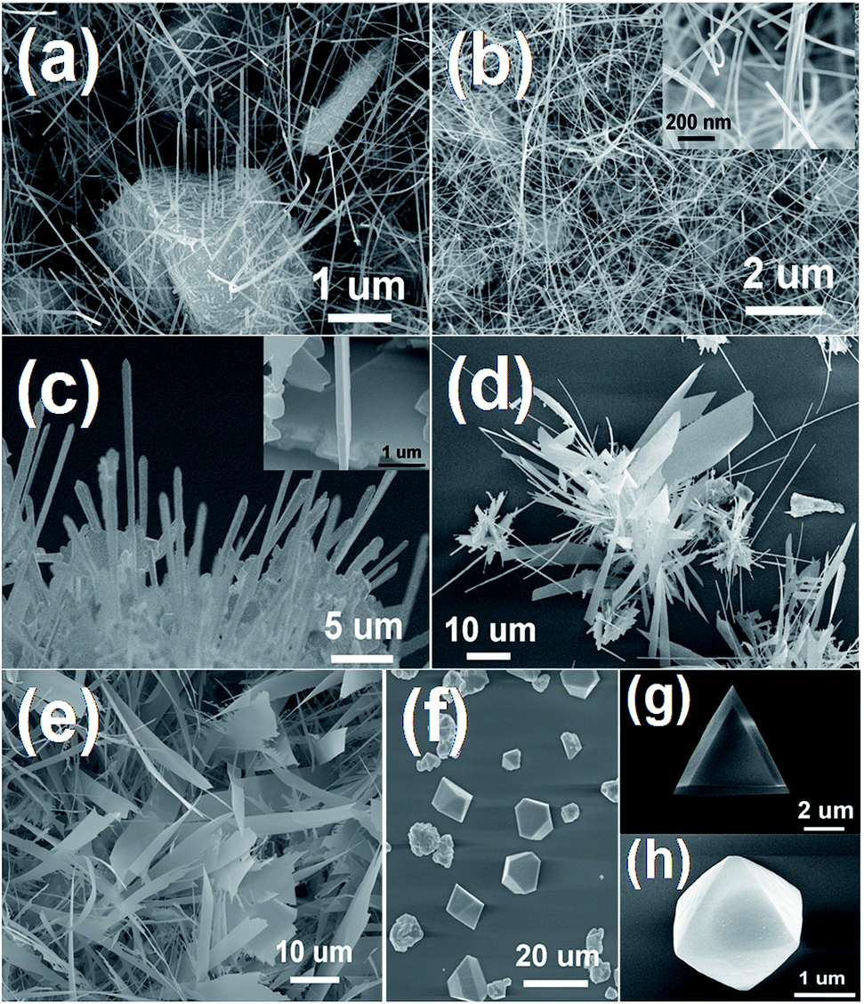 | ||
| Fig. 1 SEM images of the Cd3As2 nanostructures grown at an argon flow rate of 50 sccm. (a–c) SEM images of the Cd3As2 nanowires grown under 100 Pa, 110 Pa, and 120 Pa respectively. (d) The coexistence of Cd3As2 nanowires and nanobelts grown under 140 Pa. (e) SEM images of the Cd3As2 nanobelts grown under 150 Pa. (f–h) The Cd3As2 nanocrystals grown under a pressure over 200 Pa, in which (g) shows a typical nanoplate, (h) shows a nano-octahedron. | ||
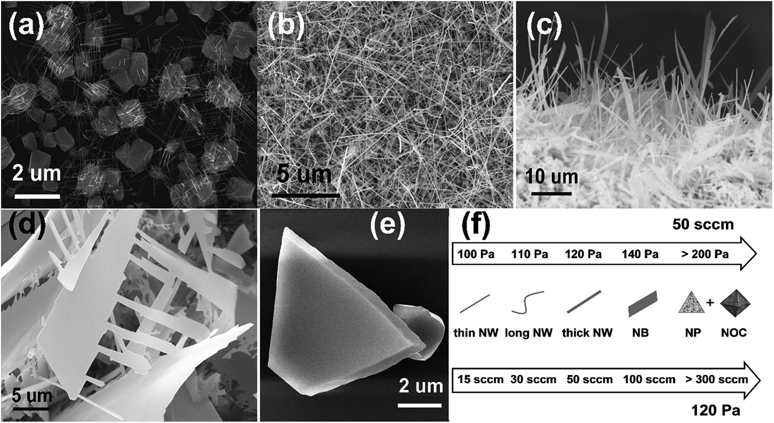 | ||
| Fig. 2 (a–e) SEM images of the Cd3As2 nanostructures grown under 120 Pa at 15 sccm, 30 sccm, 50 sccm, 100 sccm and 300 sccm, respectively. (f) Summary of the schematic morphologies of Cd3As2 nanostructures controlled by the pressure and the argon flow rate. | ||
The crystallites with a typical size of several micrometers have a pyramidal shape enclosed by {112} facets.27 The diameters of nanowires grown under 100 Pa are often less than 30 nm, and even if given adequate source and time, the nanowires are incapable of reaching a larger size. The growth time and amount of sources only determine the quantity of nanowires, having no effect on the morphology of a single nanowire.
Fig. 1(b) shows the nanowires grown under 110 Pa. The nanowires range from tens of to one hundred micrometers in length, and 20 to 100 nm in diameter. Besides, the nanowires have a large aspect ratio and show great flexibility, as shown in the inset of Fig. 1(b). The nanowires grown under 120 Pa are shown in Fig. 1(c). Compared with the nanowires shown in Fig. 1(b), nanowires here have much larger diameter, with typical width and thickness up to hundreds of nanometers. The inset of Fig. 1(c) indicates the cross-section shape of the nanowires is rectangular. When the pressure increases to 140 Pa, we generally get nanobelts and nanowires at the same time (Fig. 1(d)). The nanobelts range from tens of to one hundred micrometers in length, several micrometers to tens of micrometers in width, and hundred nanometers in thickness. Then at 150 Pa, the most visible resultants are nanobelts with little nanowires, as shown in Fig. 1(e). The appropriate pressure at a fixed argon flow of 50 sccm for the growth of nanowires and nanobelts is between 100 to 200 Pa. The resultants grown under a pressure below 100 Pa are short and thin nanowires with poor crystallization, while under a pressure above 200 Pa, the resultants are Cd3As2 nanocrystals as shown in Fig. 1(f). Fig. 1(g) and (h) show a typical faceted nanoplate and nano-octahedron, respectively.
Another important growth parameter is the gas flow rate. Though the test tube impedes the gas flow toward the source and silicon substrates immediately in our experiment, the change of argon flow rate still has influence on the circumstance in the test tube. Fig. 2(a)–(e) shows the Cd3As2 nanostructures acquired at different argon flow rate at 120 Pa. With the increase of argon flow rate, a transition from thin nanowires to broad nanobelts and nanocrystals takes place, which demonstrates that argon flow rate plays an identical role as pressure in the growth of Cd3As2 nanostructures.
During the synthesis of Cd3As2 nanostructures, it is found that varying pressure and argon flow rate has considerable control over the morphology of the resultants. The morphologies as a function of pressure and flow rate are summarized in Fig. 2(f). The enhancement of pressure and argon flow rate may accelerate the deposition rate of the evaporated source, resulting in the increase in the size and the change of morphology of Cd3As2 nanostructures.
The synthesis of nanowires can be accounted by a tip-induced vapor–solid (VS) growth mechanism,27 in which the Cd droplets serve as nucleation sites in the growth process. Cd and As atoms are evaporated and transported to the silicon substrates successively to form CdAs crystallites, which can be clearly seen in Fig. 1(a) and 2(a). And the Cd3As2 nanowires grow from the Cd-rich areas on the facets of these crystallites.27 Cd could be regarded as catalyst which leads the growth of Cd3As2 nanowires. As to the growth of nanobelts, we may notice that the lateral growth is quite prominent, which can be attributed to the well-known VS mechanism. So we conclude that the nanobelts are generated by a combination of tip induced VS growth and VS epitaxial growth. If the synthesized nanobelts have some Cd-rich areas on themselves, extra tip-induced VS growth would take place. Zigzag nanobelts like comb can be obtained under this circumstance, as seen in Fig. 2(d). In our experiment, the growth time has no significant effect on the morphologies. This might be due to the fact that the small diameter test tube accelerates the evaporated source flow rate, resulting in the rapid consumption of sources. The synthesis of Cd3As2 single crystalline nanoplates and nano-octahedra was reported by Li et al.28 The VS growth mechanism can also be used to describe the growth of these nanostructures. Compared with nanowires and nanobelts, nanoplates and nano-octahedra could be obtained under much higher pressure or argon flow rate,28 which may accelerate the As atoms deposition rate and improve the solubility limit of As in Cd, so that it is difficult to form Cd-rich areas on the synthesized microcrystals. Therefore, only epitaxial growth takes place without the Cd-rich atmosphere as catalyst.
Morphologies and good crystallinity of the synthesized nanowire and nanobelt have been verified by the TEM images and HRTEM (high resolution TEM), as shown in Fig. 3. Fig. 3(a) is a TEM image of a typical Cd3As2 nanowire with a diameter about 100 nm. And the corresponding HRTEM image with its Fourier transform of the lattice are depicted in the inset, which clearly shows a lattice spacing of 0.73 nm, indicating the growth along the [112] direction. Besides, the HRTEM image also shows a 5 nm thickness of oxidation layer, which indicates that thin nanowires are easy to be oxidized. Fig. 3(b) shows a single nanobelt with a width about 2 μm. And the inset shows the corresponding HRTEM image, which evidences a perfect crystalline structure. The lattice spacing of nanobelt is also 0.73 nm and the Fourier transform also shows [112] growth direction, consistent with the nanowire. Fig. 3(c) and (d) show the typical energy dispersive spectroscopy (EDS) spectra of a single nanowire and nanobelt, respectively. The peak of Cu in Fig. 3(d) is caused by the copper grid used for carrying the sample. Both the quantitative analyses suggest an atomic ratio of Cd/As close to 3![[thin space (1/6-em)]](https://www.rsc.org/images/entities/char_2009.gif) :2, consistent with the stoichiometry of Cd3As2. We also carried out Raman spectroscopy on a single nanowire and nanobelt. Two peaks are found at 190 and 246 cm−1, as shown in Fig. 3(e) and (f), which suggest that our nanostructures have the crystal structure of α′′-Cd3As2.25,29 Powder X-ray diffraction (XRD) of Cd3As2 nanostructures was also carried out, seen in Fig. S1 in ESI.† And the results demonstrate the I41cd symmetry structure of our Cd3As2 nanowires and nanobelts.
:2, consistent with the stoichiometry of Cd3As2. We also carried out Raman spectroscopy on a single nanowire and nanobelt. Two peaks are found at 190 and 246 cm−1, as shown in Fig. 3(e) and (f), which suggest that our nanostructures have the crystal structure of α′′-Cd3As2.25,29 Powder X-ray diffraction (XRD) of Cd3As2 nanostructures was also carried out, seen in Fig. S1 in ESI.† And the results demonstrate the I41cd symmetry structure of our Cd3As2 nanowires and nanobelts.
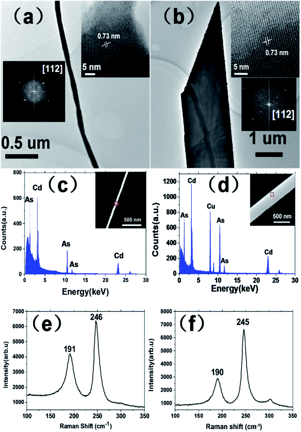 | ||
| Fig. 3 Microstructures characteristics and component analysis of Cd3As2 nanostructures. (a and b) TEM images, (c and d) EDS spectrum, and (e and f) Raman spectrum of a single Cd3As2 nanowire and nanobelt respectively. The insets in (a) and (b) show the corresponding HRTEM images with their Fourier transform images. | ||
To study the transport properties of as-grown various nanostructures, we fabricated nanodevices and carried out electrical transport measurements. Fig. 4(a) is the typical SEM image of a nanobelt device. The temperature dependence of resistance is shown in Fig. 4(b). The resistivity of nanobelt can reach several tens μΩ cm, which is comparable to the bulk of Cd3As2 materials.11,15 The resistance of Cd3As2 nanobelt exhibits an insulating behaviour at high temperature and a metallic behaviour at low temperature, which is very different from the metallic behaviour of bulk and microbelts of Cd3As2.11,14,15 The insulating behavior of RT may be caused by the light impurity doping effect, which is inevitably introduced into the nanostructures during the growth progress. The doping has great effect on the carrier density and the behavior of RT. As reported in Bi2Se3 with systematically doping Sb, the carrier density could change from 1019 cm−3 to 1016 cm−3 while the RT behavior changes from metallic to insulating.30 However, the insulating behaviour has also been observed in the Cd3As2 nanowire and can be explained by the thermal activation mechanism.22–24,26 As discussed in ref. 23, the Fermi level is higher away from the Dirac point in the bulk Cd3As2 and closer to the Dirac point in the Cd3As2 nanostructure. This results in a lower carrier density in the Cd3As2 nanostructure and hole in the valence band can be thermally activated. The Dirac cone band result a zero gap between valence and conduction band, so the holes in the valence band can be excited even at low temperature.31 Whether the insulating behavior is caused by the light doping or the low carrier density with low Fermi level need further study work, here we use the low carrier density mechanism to explain the insulating behavior temporarily. As shown in the inset of Fig. 4(b), the resistance at high temperature can be fitted by Arrhenius equation32,33 and the activation energy Δ = 31 meV can be acquired. When the temperature decreases to a certain value, electrons cannot be activated to the conduction band above the Fermi level. With continuous decreasing the temperature, whether the RT exhibit insulating or metallic behaviour depends on the residual carrier density.23 For the sample with very low residual carrier density, the insulating behaviour of RT will be observed at low temperature. On the contrary, the metallic behaviour will be observed with high residual carrier density. For different samples, the residual carrier density at low temperature has slight difference with each other. From the metallic behaviour at low temperature, we can infer that our nanobelt device has high residual carrier density. Fig. 4(c) shows the magnetoresistance measurement of nanobelt in perpendicular magnetic field at different temperatures. The magnetoresistance is almost linear and unsaturated at high magnetic field. At low temperature from 2 to 15 K, the linear magnetoresistance is almost the same, but the amplitude begins to decrease with increasing temperature. This phenomenon has been observed in single crystal and microbelts of Cd3As2.13,15,24 Different from the linear magnetoresistance reported in bulk single crystals,15 there is no Shubnikov-de Haas (SdH) oscillation superposed on the linear magnetoresistance in our nanobelt device. This indicates that the mobility of our Cd3As2 nanobelt samples is greatly suppressed when the dimension is reduced as compared with the bulk Cd3As2 materials.22,25
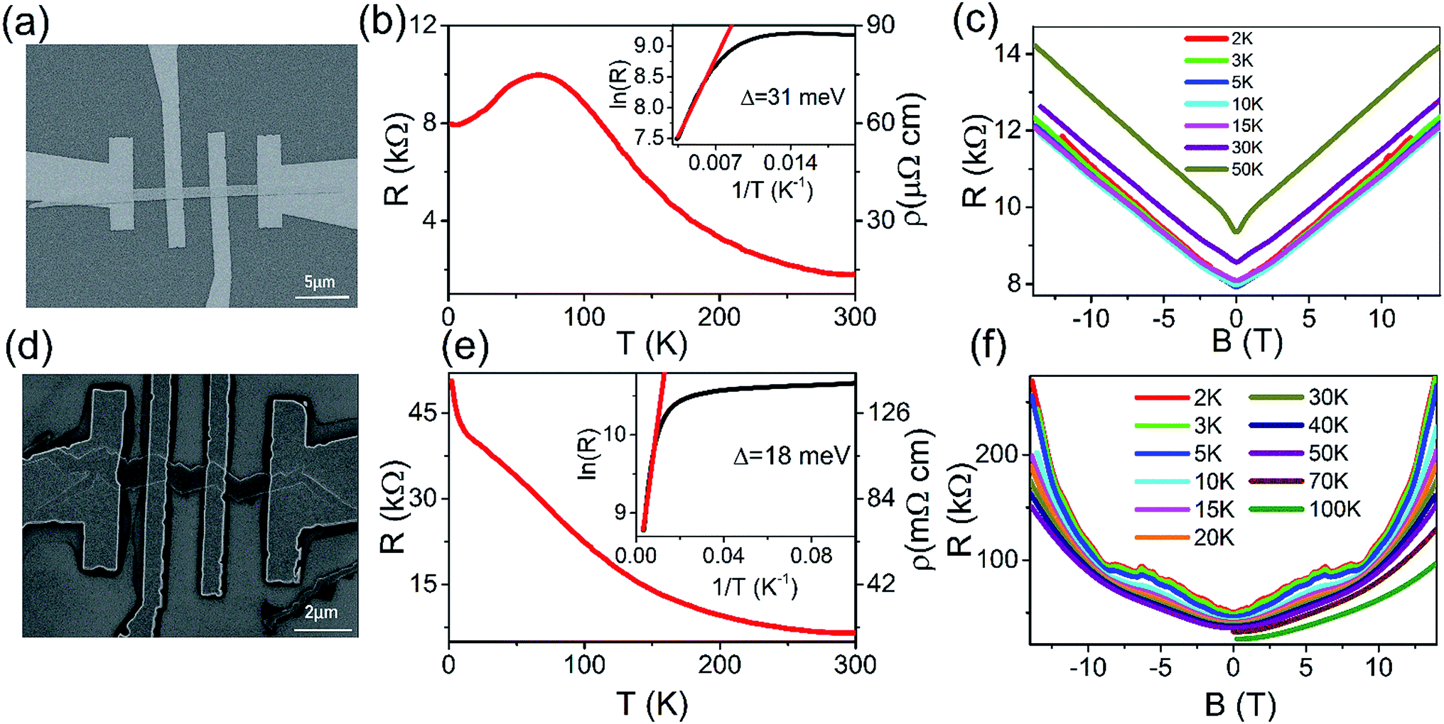 | ||
| Fig. 4 The device and electrical transport properties of two kinds of Cd3As2 nanobelts. (a–c) are related to the Cd3As2 nanobelt. (a) The SEM image of the device. (b) Temperature dependence of the resistance (left axis) and resistivity (right axis) of a Cd3As2 nanobelt. The inset shows the activation energy Δ = 31 meV by fitting the Arrhenius formula. (c) The magnetoresistance measured at different temperatures in perpendicular magnetic field. (d–f) are related to the Cd3As2 zigzag nanobelt. (d) The SEM image. (e) Temperature dependence of the resistance (left axis) and resistivity (right axis) of a Cd3As2 zigzag nanobelt. The inset shows the fitting activation energy Δ = 18 meV. (f) The magnetoresistance measured at various temperatures in perpendicular magnetic field. | ||
Fig. 4(d) displays the typical SEM image of a zigzag nanobelt device. The resistance versus temperature exhibits insulating behaviour all over the temperature scale in Fig. 4(e). The resistivity of zigzag nanobelt exhibits several tens mΩ cm, which is three orders higher than the nanobelt.11,15 Using the Arrhenius formula to analyse the R–T curve,32,33 we can obtain the activation energy Δ = 18 meV at high temperature scale in the inset of Fig. 4(e). At the temperature below 10 K, the resistance increases rapidly. As analysis in Fig. 4(b), the insulating behaviour at low temperature is due to the low residual carrier density. Fig. 4(f) is the magnetoresistance measurement of the zigzag nanobelt device. As we can see, the magnetoresistance is almost parabola at high temperature, indicating the classic magnetotransport in the nanobelt. As the temperature decreasing, the magnetoresistance starts to diverge from the parabola. Further decreasing the temperature to 10 K, the magnetoresistance begins to increase steeply in high field (>9 T). Below 5 K, there exist some clear wiggles in the magnetoresistance background and disappear rapidly as the temperature increase. The thickness of our nanobelt device is about 56 nm. In this case, the quantum confinement is prominent and this may be the reason why the wiggles exist at low temperatures.34,35 Fig. 5(a) shows the typical SEM image of Cd3As2 nanowire device. As shown in Fig. 5(b), the RT curve is the same as nanobelt and exhibits the insulating behavior. The resistivity of nanowire is almost several tens mΩ cm, which is higher than the bulk of Cd3As2 materials.11,15 The inset of Fig. 5(b) displays the activation energy Δ = 19 meV by fitting the Arrhenius formula.32,33 The resistance below 30 K increases very slowly with decreasing temperature, indicating that our nanowire device has a low residual carrier density. The magnetoresistance of nanowire device measured at 2 K is shown in Fig. 5(c). It can be clearly seen that some oscillations superposed on the linear field dependence background magnetoresistance. After subtracting the smooth linear background, the absolute oscillation can be seen in the inset of Fig. 5(c). The main frequency F = 22 T can be obtained by fast Fourier transform (FFT) spectrum. This verified the oscillation come from the quantum SdH oscillation.25,36–39 According to the Onsager relation F = (Φ0/2π2)AF, where Φ0 = h/2e and AF = πkF2, the cross section area of the Fermi surface normal to the field is AF = 2.1 × 10⁻³ Å−2 and the Fermi momentum is kF = 0.026 Å−1. The estimated carrier density is n = kF3/3π2 = 5.8 × 1017 cm−3, which is smaller than the carrier density of the Cd3As2 bulk material.15 Moreover, we measured various temperature magnetoresistance of the nanowire device. As shown in Fig. 5(d), the SdH oscillation becomes weak and even disappears when temperature is higher than 10 K. At high temperature, the magnetoresistance is almost linear and can even reach 470% (14 T) at 70 K (ESI in Fig. S2†).
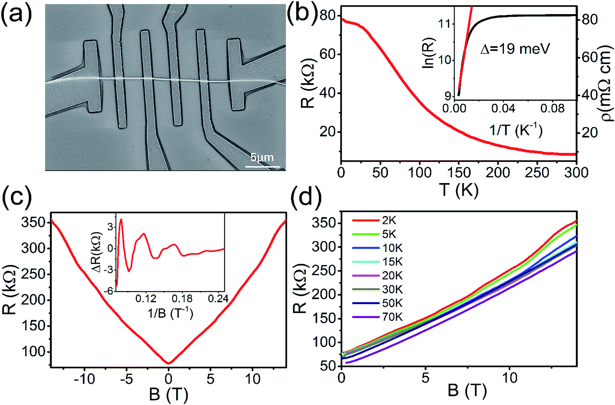 | ||
| Fig. 5 The device and electrical transport properties of a single Cd3As2 nanowire. (a) The SEM image of the nanowire device. (b) Temperature dependence of the resistance (left axis) and resistivity (right axis) of a single Cd3As2 nanowire. The inset displays the fitting activation energy Δ = 19 meV. (c) The magnetoresistance measured at 2 K in perpendicular magnetic field. The inset shows the SdH oscillation after subtracting the background. (d) The magnetoresistance measured at different temperatures in perpendicular magnetic field. | ||
From the above magnetoresistance analysis, it can be seen that three types of as-grown nanostructures all host the unsaturated magnetoresistance. The nanobelt and nanowire devices display perfect linear magnetoresistance. This may indicate that the linear and unsaturated magnetoresistance is the main property of Cd3As2 nanostructure. There are mainly two interpretation types of the linear magnetoresistance. The first interpretation type is the classical mechanism40 that the linear magnetoresistance is due to the inhomogeneous distribution of ions in the material, which results in a large spatial fluctuation in the conductivity. The Hall signal will contribute to the longitudinal resistance. From the TEM image in Fig. 3, we can confirm that the good crystalline quality of the nanobelts. Another type interpretation of the linear magnetoresistance is the quantum limit mechanism.41,42 The linear magnetoresistance will be observed when all electrons fill into the lowest n = 1 Landau level and only the lowest Landau level electrons contribute to the conductivity. Fig. 4(c) shows no SdH trace from 0 to 14 T, hence the Landau level is not formed. While from Fig. 5(c), the SdH oscillation can be seen, indicating the Landau level does not reach the lowest level. These mechanisms cannot explain our result. Recent experiments show that the linear unsaturated magnetoresistance is the particular property of Cd3As2 material. As Cd3As2 is one of the Dirac semimetal and electron can move in a free-of-backscattering way in zero magnetic field. When applying magnetic field the free-of backscattering protection mechanism will be broken and results the linear unsaturated magnetoresistance.15 As mentioned above, our nanostructures host low carrier density and the Fermi level is closer to the Dirac point compared with its bulk materials, which may benefit from the tip induced vapour–solid growth mode of our samples. In the process of heating, Cd atoms evaporate first to form Cd droplets on the substrate acting as catalyst. In the growth process, As-rich vapour impinges Cd droplets and Cd atoms diffuse from the Cd droplets to the As-rich layer to form the Cd3As2 nanostructures crystal.27 So the nanostructures of Cd3As2 grown by CVD method tend to have less As vacancies than the bulk Cd3As2 materials grown from Cd flux method. That's why the Fermi level of Cd3As2 nanostructures is close to the Dirac point with low carrier density. Although the dimension decreases in our Cd3As2 nanostructures, the linear unsaturated magnetoresistance property of its bulk material is kept in our nanostructures. This may be the reason why we observed unsaturated magnetoresistance in our Cd3As2 various nanostructures.
Conclusions
In conclusion, Cd3As2 nanostructures with different morphologies have been synthesized successfully by a facile CVD method. The morphologies can be regulated only by changing the pressure and argon flow rate. The Cd3As2 nanostructures have the good crystallinity of α′′-Cd3As2 structure. The as-grown Cd3As2 nanostructures display unsaturated magnetoresistance and linear magnetoresistance. Our research provides important information in the synthesis of various Cd3As2 nanostructures and the potential application of Cd3As2 nanodevices.Experimental section
Synthesis of Cd3As2 nanostructures
The synthesis of Cd3As2 nanostructures was performed in a single-heat zone tube furnace. Cd3As2 nanostructures were grown on silicon substrates via the VS mechanism using Cd3As2 powders (purity > 99.99, J & K Scientific) as the evaporation source. Firstly, Cd3As2 powder and silicon wafers were placed into a small open test tube. And the silicon substrates were placed close to the open end of the test tube, while the Cd3As2 powder was placed at the other end of the test tube. Then we put the test tube into the quartz tube of the furnace, making sure that the Cd3As2 powder placing at the hot centre of furnace and silicon substrates placing downstream of the source to collect the products. The tube furnace was pumped and flushed with argon several times in order to remove air and water before growth. Then the temperature was ramped to 760 °C within 15 min and maintained at 760 °C for 40 min for growth. Before taking the silicon substrates out, the system cooled down to room temperature over 2 hours under a constant argon flow.Device fabrication and measurements
The as-grown Cd3As2 nanostructures were transferred to SiO2/Si substrates to fabricate nanodevices. We used standard electron-beam lithography (EBL) technique to fabricate multi-terminal electrodes patterns above desired nanostructures. The Ti(5 nm)/Au(150 nm) alloy was deposited to the patterns by electron beam evaporation. Then followed by standard lift off, final nanodevices were fabricated. We used four-probe electrodes to measure the resistance of nanodevices. The magnetoresistance measurement was carried out in the Quantum Design Physical Property Measurement System-16T system.Acknowledgements
We gratefully acknowledge the financial support from the National Key Projects for Basic Research of China (Grant No. 2013CB922103 and 2014CB921103), the National Natural Science Foundation of China (Grant No. 91421109, 11274003, 11134005, 11522432, and 11574288), and the Fundamental Research Funds for the Central Universities.Notes and references
- X. Wan, A. M. Turner, A. Vishwanath and S. Y. Savrasov, Phys. Rev. B: Condens. Matter Mater. Phys., 2011, 83, 205101 CrossRef.
- Z. Wang, H. Weng, Q. Wu, X. Dai and Z. Fang, Phys. Rev. B: Condens. Matter Mater. Phys., 2013, 88, 125427 CrossRef.
- Z. Wang, Y. Sun, X.-Q. Chen, C. Franchini, G. Xu, H. Weng, X. Dai and Z. Fang, Phys. Rev. B: Condens. Matter Mater. Phys., 2012, 85, 195320 CrossRef.
- S. M. Young, S. Zaheer, J. C. Teo, C. L. Kane, E. J. Mele and A. M. Rappe, Phys. Rev. Lett., 2012, 108, 140405 CrossRef CAS PubMed.
- Z. K. Liu, B. Zhou, Y. Zhang, Z. J. Wang, H. M. Weng, D. Prabhakaran, S.-K. Mo, Z. X. Shen, Z. Fang, X. Dai, Z. Hussain and Y. L. Chen, Science, 2014, 343, 864–867 CrossRef CAS PubMed.
- S.-y. Xu, I. Belopolski, N. Alidoust, M. Neupane, G. Bian, C. Zhang, R. Sankar, G. Chang, Z. Yuan, C.-C. Lee, S.-M. Huang, H. Zheng, J. Ma, D. S. Sanchez, B. Wang, A. Bansil, F. Chou, P. P. Shibayev, H. Lin, S. Jia and M. Z. Hasan, Science, 2015, 349, 613–617 CrossRef CAS PubMed.
- E. V. Gorbar, V. A. Miransky and I. A. Shovkovy, Phys. Rev. B: Condens. Matter Mater. Phys., 2013, 88, 165105 CrossRef.
- M. Neupane, S. Y. Xu, R. Sankar, N. Alidoust, G. Bian, C. Liu, I. Belopolski, T. R. Chang, H. T. Jeng, H. Lin, A. Bansil, F. Chou and M. Z. Hasan, Nat. Commun., 2014, 5, 3786 CAS.
- Z. K. Liu, J. Jiang, B. Zhou, Z. J. Wang, Y. Zhang, H. M. Weng, D. Prabhakaran, S. K. Mo, H. Peng, P. Dudin, T. Kim, M. Hoesch, Z. Fang, X. Dai, Z. X. Shen, D. L. Feng, Z. Hussain and Y. L. Chen, Nat. Mater., 2014, 13, 677–681 CrossRef CAS PubMed.
- Z. G. Chen, C. Zhang, Y. Zou, E. Zhang, L. Yang, M. Hong, F. Xiu and J. Zou, Nano Lett., 2015, 15, 5830–5834 CrossRef CAS PubMed.
- L. P. He, X. C. Hong, J. K. Dong, J. Pan, Z. Zhang, J. Zhang and S. Y. Li, Phys. Rev. Lett., 2014, 113, 246402 CrossRef CAS PubMed.
- Z. J. Xiang, D. Zhao, Z. Jin, C. Shang, L. K. Ma, G. J. Ye, B. Lei, T. Wu, Z. C. Xia and X. H. Chen, Phys. Rev. Lett., 2015, 115, 226401 CrossRef CAS PubMed.
- J. Feng, Y. Pang, D. Wu, Z. Wang, H. Weng, J. Li, X. Dai, Z. Fang, Y. Shi and L. Lu, Phys. Rev. B: Condens. Matter Mater. Phys., 2015, 92, 081306 CrossRef.
- Y. Zhao, H. Liu, C. Zhang, H. Wang, J. Wang, Z. Lin, Y. Xing, H. Lu, J. Liu, Y. Wang, S. M. Brombosz, Z. Xiao, S. Jia, X. C. Xie and J. Wang, Phys. Rev. X, 2015, 5, 031037 Search PubMed.
- T. Liang, Q. Gibson, M. N. Ali, M. Liu, R. J. Cava and N. P. Ong, Nat. Mater., 2015, 14, 280–284 CrossRef CAS PubMed.
- J. Cao, S. Liang, C. Zhang, Y. Liu, J. Huang, Z. Jin, Z. G. Chen, Z. Wang, Q. Wang, J. Zhao, S. Li, X. Dai, J. Zou, Z. Xia, L. Li and F. Xiu, Nat. Commun., 2015, 6, 7779 CrossRef PubMed.
- H. Wang, H. Wang, H. Liu, H. Lu, W. Yang, S. Jia, X.-J. Liu, X. C. Xie, J. Wei and J. Wang, Nat. Mater., 2016, 15, 38–42 CrossRef CAS PubMed.
- L. Aggarwal, A. Gaurav, G. S. Thakur, Z. Haque, A. K. Ganguli and G. Sheet, Nat. Mater., 2016, 15, 32–37 CrossRef CAS PubMed.
- L. He, Y. Jia, S. Zhang, X. Hong, C. Jin and S. Li, NPJ Quantum Mater., 2016, 1, 16014 CrossRef.
- A. Narayanan, M. D. Watson, S. F. Blake, N. Bruyant, L. Drigo, Y. L. Chen, D. Prabhakaran, B. Yan, C. Felser, T. Kong, P. C. Canfield and A. I. Coldea, Phys. Rev. Lett., 2015, 114, 117201 CrossRef CAS PubMed.
- H. Jin, Y. Dai, Y.-D. Ma, X.-R. Li, W. Wei, L. Yu and B.-B. Huang, J. Mater. Chem. C, 2015, 3, 3547–3551 RSC.
- E. Zhang, Y. Liu, W. Wang, C. Zhang, P. Zhou, Z. G. Chen, J. Zou and F. Xiu, ACS Nano, 2015, 9, 8843–8850 CrossRef CAS PubMed.
- C. Z. Li, L. X. Wang, H. Liu, J. Wang, Z. M. Liao and D. P. Yu, Nat. Commun., 2015, 6, 10137 CrossRef CAS PubMed.
- H. Li, H. He, H. Z. Lu, H. Zhang, H. Liu, R. Ma, Z. Fan, S. Q. Shen and J. Wang, Nat. Commun., 2016, 7, 10301 CrossRef CAS PubMed.
- H. Pan, K. Zhang, Z. Wei, B. Zhao, J. Wang, M. Gao, L. Pi, M. Han, F. Song, X. Wang, B. Wang and R. Zhang, Appl. Phys. Lett., 2016, 108, 183103 CrossRef.
- L.-X. Wang, C.-Z. Li, D.-P. Yu and Z.-M. Liao, Nat. Commun., 2016, 7, 10769 CrossRef CAS PubMed.
- P. Schönherr and T. Hesjedal, Appl. Phys. Lett., 2015, 106, 013115 CrossRef.
- C.-Z. Li, R. Zhu, X. Ke, J.-M. Zhang, L.-X. Wang, L. Zhang, Z.-M. Liao and D.-P. Yu, Cryst. Growth Des., 2015, 15, 3264–3270 CAS.
- S. Wei, J. Lu, W. Yu, H. Zhang and Y. Qian, Cryst. Growth Des., 2006, 6, 849–853 CAS.
- J. G. Analytis, R. D. McDonald, S. C. Riggs, J.-H. Chu, G. S. Boebinger and I. R. Fisher, Nat. Phys., 2010, 6, 960–964 CrossRef CAS.
- J. Xiong, S. K. Kushwaha, T. Liang, J. W. Krizan, W. Wang, R. J. Cava and N. P. Ong, 2015, arXiv:1503.08179.
- Z. Ren, A. A. Taskin, S. Sasaki, K. Segawa and Y. Ando, Phys. Rev. B: Condens. Matter Mater. Phys., 2010, 82, 241306 CrossRef.
- F. Xiu, L. He, Y. Wang, L. Cheng, L.-T. Chang, M. Lang, G. Huang, X. Kou, Y. Zhou, X. Jiang, Z. Chen, J. Zou, A. Shailos and K. L. Wang, Nat. Nanotechnol., 2011, 6, 216–221 CrossRef CAS PubMed.
- Z. Li, T. Chen, H. Pan, F. Song, B. Wang, J. Han, Y. Qin, X. Wang, R. Zhang, J. Wan, D. Xing and G. Wang, Sci. Rep., 2012, 2, 595 Search PubMed.
- L.-X. Wang, S. Wang, J.-G. Li, C.-Z. Li, D. Yu and Z.-M. Liao, Phys. Rev. B: Condens. Matter Mater. Phys., 2016, 94, 161402 CrossRef.
- K. Eto, Z. Ren, A. A. Taskin, K. Segawa and Y. Ando, Phys. Rev. B: Condens. Matter Mater. Phys., 2010, 81, 195309 CrossRef.
- D.-X. Qu, Y. S. Hor, J. Xiong, R. J. Cava and N. P. Ong, Science, 2010, 329, 821 CrossRef CAS PubMed.
- M. Zhang, X. Wang, S. Zhang, Y. Gao, Z. Yu, X. Zhang, M. Gao, F. Song, J. Du, X. Wang, L. He, Y. Xu and R. Zhang, IEEE Electron Device Lett., 2016, 37, 1231–1233 Search PubMed.
- X. Wang, X. Pan, M. Gao, J. Yu, J. Jiang, J. Zhang, H. Zuo, M. Zhang, Z. Wei, W. Niu, Z. Xia, X. Wan, Y. Chen, F. Song, Y. Xu, B. Wang, G. Wang and R. Zhang, Adv. Electron. Mater., 2016, 2, 1600228 CrossRef.
- M. M. Parish and P. B. Littlewood, Nature, 2003, 426, 162–165 CrossRef CAS PubMed.
- A. A. Abrikosov, Phys. Rev. B: Condens. Matter Mater. Phys., 1998, 58, 2788–2794 CrossRef CAS.
- A. A. Abrikosov, Phys. Rev. B: Condens. Matter Mater. Phys., 2000, 61, 7770–7774 CrossRef CAS.
Footnotes |
| † Electronic supplementary information (ESI) available. See DOI: 10.1039/c7ra02847d |
| ‡ These authors contributed equally to this work. |
| This journal is © The Royal Society of Chemistry 2017 |