
 Open Access Article
 This Open Access Article is licensed under a
 Creative Commons Attribution 3.0 Unported Licence
Integrated design of a Ni thin-film electrode on a porous alumina template for affordable and high-performance low-temperature solid oxide fuel cells†
Sanghoon Ji‡
abc,
Han Gil Seo‡a,
Siwon Leea,
Jongsu Seoa,
Yeageun Leed,
Waqas Hassan Tanveerd,
Suk Won Chad and
WooChul Jung *a
*a
aDepartment of Materials Science and Engineering, Korea Advanced Institute of Science and Technology, Daehak-ro, Yuseong-gu, Daejeon 34141, Republic of Korea. E-mail: wcjung@kaist.ac.kr; Fax: +82-42-350-3310; Tel: +82-42-350-3314
bApplied Science Research Center, Korea Advanced Institute of Science and Technology, Daehak-ro, Yuseong-gu, Daejeon 34141, Republic of Korea
cFuture Strategy & Convergence Research Institute, Korea Institute of Civil Engineering and Building Technology, Goyangdae-ro, Ilsanseo-gu, Goyang-si, Gyeonggi-do 10223, Republic of Korea
dDepartment of Mechanical and Aerospace Engineering, Seoul National University, Gwanak-ro, Gwanak-gu, Seoul 08826, Republic of Korea
First published on 2nd May 2017
Abstract
Nanostructured Ni thin films, with high porosity, are fabricated by DC sputtering on an anodic aluminum oxide template as an active anode for low-temperature solid oxide fuel cells with a target operating temperature of 500 °C. To maximize the electrode performance, we control their effective electrical conductivity and microstructure by varying the sputtering parameters (e.g., the deposition pressure and time) and investigate the gas permeability, sinterability, as well as the ohmic and polarization resistances by a range of analysis techniques, in this case SEM, TEM, mass spectrometry, the four-point probe method and AC impedance spectroscopy. We observe that the thicker the Ni film, the higher the effective electrical conductivity and the lower the sheet resistance, while the thinner the film, the better the gas permeability and electrochemical activity for H2 electro-oxidation. These tradeoffs are quantitatively computed for cell dimensions and area specific resistances, thus suggesting an optimal design for affordable and high-performance electrodes.
1. Introduction
Solid oxide fuel cells (SOFCs) are a promising electrochemical device to produce electricity directly from chemical fuels due to their high conversion efficiency, wide range of fuel flexibility, and low emissions. Furthermore, in contrast to other fuel cells, they do not require complicated water management schemes or the use of precious metal catalysts, thus lowering the production costs.1,2 Despite these advantages, however, the excessively high operating temperatures, typically over 800 °C, and the resulting material and cost limitations and operating complexities significantly limit their applications only to cumbersome and immobile electricity production units (e.g., stationary power plants and uninterruptible power supply units).In an effort to reduce the operating temperature (<600 °C), thin-film-based SOFCs composed of a dense thin film of solid oxide electrolyte between porous electrode films have been actively studied over the past years.3–7 The use of a thin electrolyte membrane can substantially reduce the ohmic resistance, and a nanostructured thin-film electrode can also accelerate electrochemical reactions. Consequently, a number of researchers demonstrated thin-film SOFCs with decent power density levels, in some cases around 1 W cm−2 even at temperatures as low as 450 °C.4,6 Thus far, most thin-film-based SOFCs reported in the literature have been fabricated in the form of free-standing membranes on Si wafers through micro-fabrication processes which generally include thin-film deposition, photolithographic patterning, and chemical etching steps. However, in this architecture, scaling up remains a significant challenge because large-area free-standing membranes are highly susceptible to mechanical failure at elevated temperatures (e.g., buckling and/or fracturing).
Recently, in this regard, researchers have deposited membrane electrode assemblies directly onto a porous support which is mechanically robust, chemically resistant, and suitable for scaling up.8 Among several promising support materials such as patterned nickel foil, porous cermet or machined glass ceramics,9–11 the anodic aluminum oxide (AAO) template has gained a considerable amount of attention because it is inexpensive, easy to manufacture over a large area, and even offers precise control of the pore size.12,13 Furthermore, AAO templates are chemically stable under redox cycling conditions at elevated temperatures, in contrast to typical Ni metal or cermet materials.14 However, at present, a key technical issue preventing the use of the AAO template as a porous support material for thin-film SOFCs is the lack of the electrical conductivity of AAO itself and the ensuing difficulty in current collection through electrode. This is particularly important because in the structure in which the electrode is sandwiched between the electrolyte and the support, referred to the ASE (AAO-supporting electrode), there is no room for an additional current collector (see Fig. 1).15
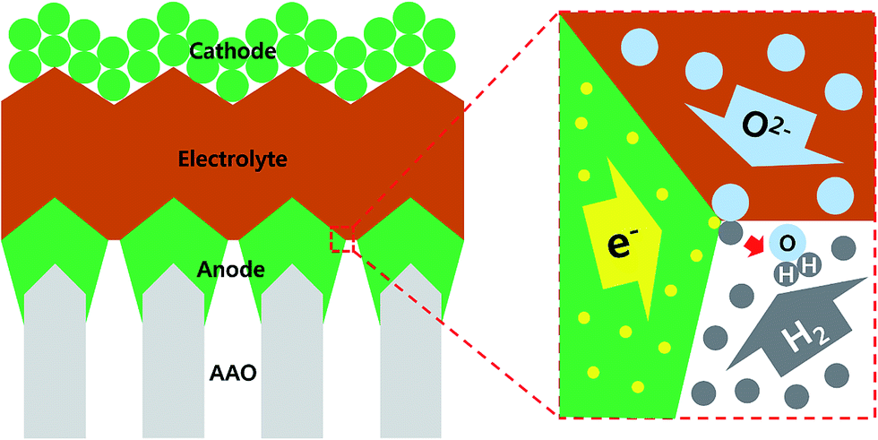 | ||
| Fig. 1 A schematic image showing the structure of a thin-film-based solid oxide fuel cell supported on an anodic aluminum oxide (AAO) template and the transport of gases, oxygen ions and electrons near the electrodes and the electrolyte. | ||
Ni can be a good choice for an ASE material; it is a good electronic conductor and a favorable catalyst for hydrogen electro-oxidation – a typical fuel cell anode reaction. More importantly, it is cheap and earth-abundant, in contrast to precious metals (e.g., Pt or Pd, the state-of-the-art electrode material for thin-film SOFCs).16,17 However, although the problem of Ni oxidation, which arises during typical operating conditions and which was a main obstacle to the use of Ni, has recently been solved by system-level solutions such as gas recirculation and/or partial oxidation,18 few studies in the literature report attempts to use porous Ni films as an ASE for low-temperature SOFCs (LT-SOFCs). Previously, we successfully fabricated submicron-thick Ni ASEs by means of DC sputtering and confirmed their feasibility for thin-film-based SOFCs at a target operating temperature of approximate 500 °C.19,20 However, these studies were performed under arbitrarily selected deposition conditions and film microstructures. To the best of our knowledge, there is no systematic study of the relationship between the deposition conditions, microstructures, and electrode performances of Ni ASEs for LT-SOFCs.
In this work, we fabricated submicron-thick porous Ni films on an AAO template with a pore size of ∼60 nm as an ASE by DC sputtering and controlled their effective electrical conductivity and microstructure by varying the deposition pressure and time. By examining the effective electrical conductivity change of the Ni thin film under different deposition pressures, the optimal deposition pressure of 4 mTorr (Ar) was initially selected. We then investigated how the morphology of the Ni thin film ASEs varied with the thickness and how the sheet resistance and gas permeability changed accordingly. Finally, we fabricated a full cell with the following composition: AAO support|Ni ASE|yttria-stabilized zirconia (YSZ) electrolyte|Pt cathode. Subsequently, we evaluated the change in both the in-plane ohmic and polarization resistance values of the Ni ASEs according to the thickness by AC impedance spectroscopy (ACIS). It was found that thicker films have better current collecting capacities whereas thinner ones show improved gas permeability and better electrochemical catalysis. Based on the consideration of these tradeoffs with regard to cell dimension and area specific resistance (ASR) values, we suggest a means of fabricating affordable high-performance electrodes for LT-SOFCs.
2. Experimental
2.1 Sample preparation
The 10 × 10 mm square-shaped, 100 μm-thick AAO templates (Synkera Technologies, USA) with a pore size of ∼60 nm and a volumetric density of ∼13% were used as the supporting structure for Ni thin films. Prior to Ni deposition, they were heat-treated at 700 °C and then ultra-sonicated in acetone. Porous Ni films were deposited by DC magnetron sputtering (A-Tech System, Korea), at a DC power of 100 W, from a three-inch diameter metallic target of highly pure Ni (Taewon Scientific, Korea). The total chamber pressure during deposition was varied in a range between 4 and 48 mTorr after pumping the background pressure down to less than 1 × 10⁻³ mTorr. Samples with a full cell structure (AAO|Ni|YSZ|Pt) were fabricated by the subsequent deposition of a dense YSZ thin film and a porous Pt thin film with a stainless steel (SS) shadow mask (8 × 8 mm2 for YSZ and 1 × 1 mm2 for Pt) by RF and DC sputtering, respectively. Highly pure metal targets of Zr0.84Y0.16 and Pt were used. The sputtering was undertook in a power of 200 W and a deposition pressure of 5 mTorr and 50 mTorr, respectively for YSZ and Pt. Ar was used as the working gas in sputtering. For YSZ deposition, O2 used as an oxidizing agent was additionally introduced into the chamber at a volumetric ratio of 8![[thin space (1/6-em)]](https://www.rsc.org/images/entities/char_2009.gif) :2 Ar to O2.
:2 Ar to O2.
2.2 Physical and chemical characterization
The microstructure of Ni thin films were characterized by field emission scanning electron microscopy (FE-SEM, S-4800, Hitachi, Japan) and transmission electron microscopy (TEM, Tecnai G2 F30 S-Twin, FEI, Netherlands). Four-point probe method was taken using a multimeter (Keithley 236, Tektronics, USA) and a 1 mm tip-spacing probe (M4P 205, MS-Tech, Korea) in ambient air.2.3 Gas permeability experiment
H2 permeation tests were performed by placing Ni ASEs into a custom-designed SS holder and sealing them with Si paste (CP 4010, Aremco Products, USA). Here, the concentration of permeated H2 was measured by quadrupole mass spectrometry using a GSD 320 O1 instrument (Pfeiffer Vacuum, Germany), while the chamber pressure was kept constant at 1 × 10⁻³ mTorr by turbo pumping.21 The flow rate of H2 was controlled to the values correspond to stoichiometry range of 1.5–3.5 (e.g., 12.6 sccm of H2 at a stoichiometry of 1) at 1 A cm−2 in consideration of its volumetric density at a target operating temperature of 500 °C, while maintaining the entire flow rate of 100 sccm balanced with Ar gas. The ion current intensities arising from the H2 concentrations of collected mixtures became steady in 300 s for all samples.2.4 Analysis of ohmic and polarization resistances
The spreading resistances of YSZ-coated Ni ASEs were measured by a multimeter (NI 9206, National Instruments, Korea) with four Ag-coated Cu wires under H2 atmosphere at 500 °C. For polarization resistance measurements, full cells of AAO|Ni|YSZ|Pt were placed in a custom-designed SS holder, sealed by Si paste, and then annealed in a chamber equipped with U-shaped 6 kW halogen lamps at temperatures of 450 °C and 500 °C under 25 sccm H2/air atmospheres. ACIS (1260A/1287A, Solartron Analytical, UK) was conducted in the frequency range 2 Hz–2 MHz with a AC amplitude of 50 mV at both open circuit voltage and 0.5 V-biased conditions.3. Results and discussion
3.1 Effective electrical conductivity of Ni ASE vs. the deposition pressure
Due to the electrical insulating nature of the AAO support, a metallic film with excellent electrical conductivity is required for large-area current collection and to reduce the ASE sheet resistance through it. For this reason, we initially confirmed the change in the effective electrical conductivity of Ni thin films with the deposition pressure. Fig. 2a shows how the effective electrical conductivity of both dense and porous Ni films deposited on a 300 nm-thick SiO2-coated single-crystal polished Si substrate and an AAO template, respectively, changes with the deposition pressure. It was observed that as the deposition pressure decreases, the effective electrical conductivity of the Ni films continuously increases. For example, the effective electrical conductivity of the Ni film deposited on Si at 48 mTorr is approximately 50 times lower than the bulk value of 14.3 × 10⁴ S cm−1, but when the deposition pressure is lowered to 4 mTorr, the value greatly rises to 3.5 × 10⁴ S cm−1 (Fig. 2a). It should be noted that when the deposition pressure is less than 4 mTorr, severe delamination of the Ni film occurs. For this reason, these conditions are not considered in this study.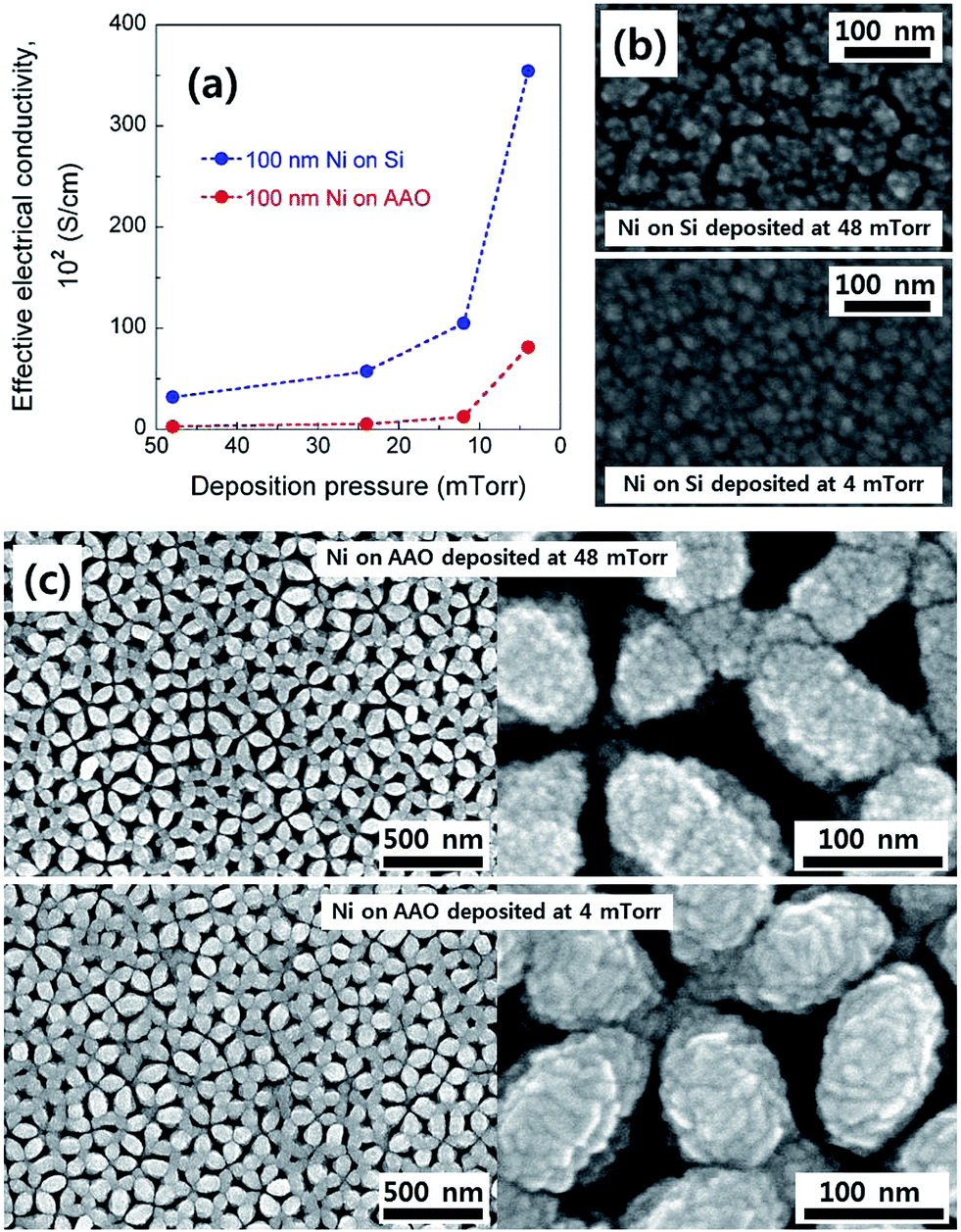 | ||
| Fig. 2 (a) Effective electrical conductivity of 100 nm-thick Ni thin films deposited on a Si substrate and an AAO template with deposition pressure between 4 and 48 mTorr. (b and c) Field emission scanning electron microscopy (FE-SEM) top-view images of 100 nm-thick Ni thin films deposited on (b) a Si substrate and (c) an AAO template at deposition pressure of 48 (upper) and 4 mTorr (lower). | ||
The change in the effective electrical conductivity according to the deposition pressure can be understood as a change in the grain boundary density and the degree of partial oxidation of Ni films.22–26 Fig. 2b exhibits FE-SEM top-view images of dense Ni thin films deposited on Si at two different deposition pressures (4 and 48 mTorr). It is clear that a higher deposition pressure level leads to a smaller size of the Ni grains with more grain boundaries. Given that electrons are scattered by the presence of grain boundaries in a metal, the effective electrical conductivity is expected to decrease with the deposition pressure, which is consistent with our observations.
Turning to the porous Ni films on the AAO support, a similar correlation was observed between the effective electrical conductivity and the deposition pressure with a maximum effective electrical conductivity of 0.8 × 10⁴ S cm−1 at 4 mTorr. However, the absolute values of the effective electrical conductivity are generally lower compared to those of the dense films, likely due to the poor connectivity of the porous columnar films. Fig. 2c shows FE-SEM top-view images of porous Ni films on AAO at deposition pressures of 4 and 48 mTorr. Both films have a well-arrayed porous microstructure, resembling the topology of the AAO template. In particular, we observed that reducing the deposition pressure causes Ni to be more conformably deposited and improves the connectivity between the Ni columns. Ultimately, 4 mTorr was selected as the deposition pressure at which the effective electrical conductivity was maximized in this study.
3.2 Morphology and gas permeability of Ni ASE vs. the thickness
As the deposition time increases, the Ni column thickens and its radius increases. At the same time, the contact between the surrounding Ni columns is increased accordingly. Fig. 3a shows a TEM cross-sectional image of Ni film deposited onto AAO. Inversely conical-shaped Ni columns with an inclination angle (θ) of approximate 4° to 6° from the vertical direction can be observed. This inclined growth is mainly due to the shadowing effects stemming from the deviation between the incidence direction to the AAO pore wall and the perpendicular direction to the substrate.27 To make continuous electrical pathways, the Ni film should be thick enough such that the neighboring Ni columns are intimately connected. On the other hand, if the thickness of the deposited Ni film is too thick, it will cover most of the AAO surface and will not easily permeate the gas. Indeed, we geometrically calculated the thickness of a thin film which can completely cover 60 nm diameter pores with inclination angles of 4° to 6°, that is, between 285 and 430 nm. As shown in Fig. 3b, only small gas channels were detectable for the 300 nm-thick Ni ASE, while in the case of the 400 nm-thick film, nearly the entire surface of the AAO template is covered by Ni. In this regard, the gas permeability through Ni ASE was quantitatively measured, as discussed below.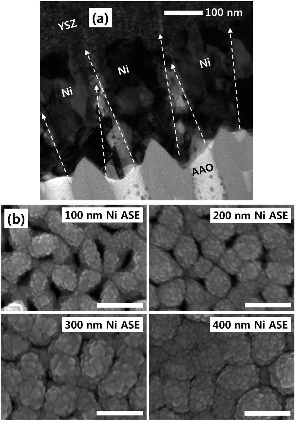 | ||
| Fig. 3 (a) A transmission electron microscopy cross-sectional image showing the inclined growth of individual Ni columns deposited on an AAO template (YSZ stands for yttria-stabilized zirconia), (b) FE-SEM top-view images of Ni thin films deposited on an AAO template with thickness between 100 and 400 nm (ASE: AAO-supporting electrode). All scale bars indicate 200 nm. | ||
The gas permeability of an electrode is a key factor in determining the current density and thus the power density of fuel cells. This is especially important for thin-film fuel cells, with which it is difficult to deliver fuel at high pressure. Here, we undertook a mass spectrometry analysis to determine how the H2 permeability changes with the thickness of the Ni ASE (Fig. 4a). Fig. 4b shows a plot between input and leakage flow rates according to the thickness. The 100 nm-thick Ni ASE exhibits permeation behavior nearly identical to that of a bare AAO template at all supply levels, indicating that sufficient pore channels are present. On the other hand, as the film thickens, the amount of gas passing through the Ni ASE is appreciably reduced, as previously predicted from the TEM imaging result. Finally, no hydrogen was detected in the 400 nm-thick Ni ASE. The average permeation yield, defined as the ratio of leakage flow rate and input flow rate, is greater than 0.8 for Ni ASEs up to 200 nm-thick but drops sharply to 0.3 at 300 nm (Fig. 4c). Therefore, in this study, the maximum apparent thickness of the Ni ASE was set to 250 nm for sufficient gas permeation.
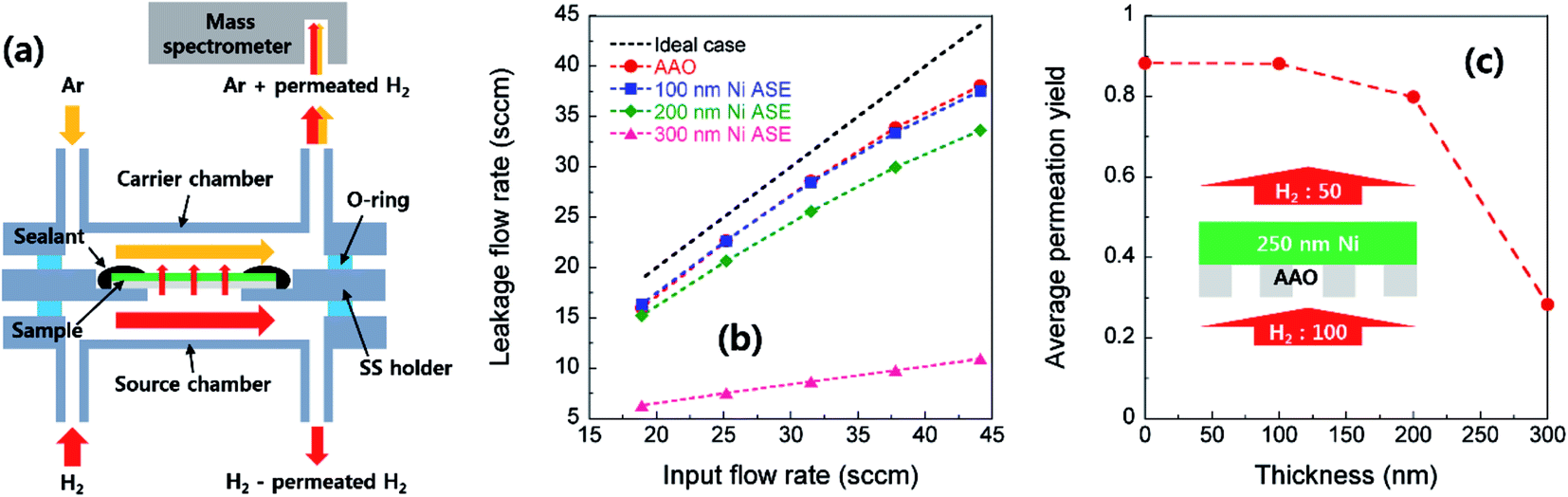 | ||
| Fig. 4 (a) A schematic image showing a stainless steel (SS) dual-chamber system with a mass spectrometer for measuring the H2 permeability of Ni ASE, (b) H2 leakage flow rate versus H2 input flow rate and (c) average permeation yield for a bare AAO template and AAO templates with 100 to 300 nm-thick Ni deposited. | ||
3.3 In-plane ohmic and polarization resistances of Ni ASE vs. the thickness
Next, we measured the electrical resistance of the Ni ASE in the in-plane direction at 500 °C according to the film thickness before/after depositing the YSZ electrolyte (Fig. 5a). The values of in-plane ohmic resistance and effective electrical conductivity of the Ni ASEs, measured between 50 and 250 nm, the lower and upper limits of the aforementioned Ni thickness, are shown in Fig. 5b. It can be seen that the in-plane ohmic resistance decreases as the Ni ASE thickness increases. It is natural that the resistance value of the thin film is inversely proportional to the thickness. However, in this case, as the thickness increases, the effective electrical conductivity also increases such that the overall resistance decreases more sharply from the linear tendency. It should be noted that the resistance value of Ni ASE was fairly stable at 500 °C at all measured thicknesses (Fig. 5c). This is most likely due to the increased sintering resistance of the constrained Ni film between the AAO and YSZ.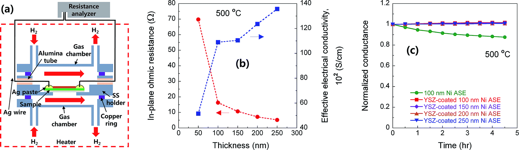 | ||
| Fig. 5 (a) A schematic image showing a dual-chamber system with a multimeter for measuring the spreading resistance of Ni ASE, (b) effective electrical conductivity and in-plane ohmic resistance of Ni ASEs (50–250 nm-thick) according to thickness measured at 500 °C, and (c) changes in the normalized conductance of Ni ASE (100 nm-thick) and YSZ-coated Ni ASEs (100–250 nm-thick). | ||
The polarization resistances of the Ni ASEs with thicknesses of 100 and 250 nm were also measured after fabricating a full cell of AAO|Ni|YSZ|Pt at both 450 and 500 °C under H2/air atmospheres (see Fig. 6a, S1 and S2†). The selected ACIS results obtained at 450 °C are presented in Fig. 6b. The overall impedance spectra, plotted in Nyquist form, are largely determined by a very large, slightly distorted semicircle at low frequencies. On the other hand, and there is a small amount of off-set resistance and one semicircle in the high-frequency region, mainly due to the combination of the YSZ ionic resistance and the Ni sheet resistance, and the YSZ grain boundary resistance, respectively.28 Indeed, the dielectric constant values calculated in the capacitive part of the high-frequency impedance are in good agreement with those of the nanocrystalline YSZ grain boundary, as reported in the literature.29,30 Focusing on the main impedance arc at low frequencies, the resistance value varies greatly with the applied voltage, and the capacitance value itself is very large, which indicates a general electrode reaction. Accordingly, this impedance response was modelled using two RQ sub-circuits of Fig. 6c (i.e., with each representing the anode and the cathode), where Q is a constant-phase element with impedance ZQ equal to 1/Q(iω)n, n is a constant, and ω is the frequency. As shown in Fig. 6d and e, only one of the two RQ sub-circuits (the one at a higher frequency) changes sensitively according to the thickness of the Ni film. Accordingly, we concluded that the higher frequency arc is attributed to the anode impedance response. Indeed, considering that the hydrogen electro-oxidation at Ni/YSZ electrode is faster than the oxygen electro-reduction at Pt/YSZ, it is common for anode impedance spectra to appear at higher frequencies than cathode ones in general. For confirmation, we carefully fabricated lithographically patterned Ni/YSZ and Pt/YSZ thin-film electrodes and measured their electrochemical impedance spectra under the conditions similar to this study (Fig. S3 and Table S1†). We observed that the hydrogen electro-oxidation of the symmetric Ni|YSZ|Ni cell is faster than the oxygen electro-reduction of the Pt|YSZ|Pt cell more than by a factor of ~7. Furthermore, the electrolyte-area normalized double layer capacitance of the Ni|YSZ|Ni cell is smaller than that of the Pt|YSZ|Pt cell around 10 times. Taking all above mentioned into account, the red arcs at higher frequencies can be thought of the Ni anode response. Therefore, we could extract the polarization resistance of Ni ASE rationally. In fact, this fitting result is consistent with our previously reported result.19 Hence, it can be seen that the electrode polarization resistance decreases as the Ni ASE thickness decreases. For example, the polarization resistance of the 100 nm-thick NI ASE is approximately two times smaller than that when the thickness is 250 nm. This is most likely due to the shape of the Ni columns, which have a larger radius as the thickness increases, and the resulting decrease in the triple phase boundary length near the Ni/YSZ interface.
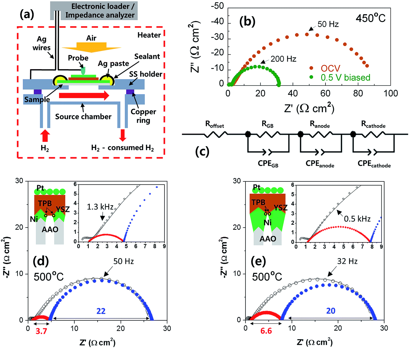 | ||
| Fig. 6 (a) A schematic image showing a dual-chamber system with AC impedance spectroscopy (ACIS) for measuring the polarization resistance of Ni ASE, (b) impedance spectra of the full cell with a 100 nm-thick Ni ASE measured at 450 °C under open circuit voltage (OCV) and 0.5 V, (c) an equivalent circuit used for ACIS analysis, and (d and e) impedance spectra of the full cell with (d) a 100 nm-thick Ni ASE and (e) a 250 nm-thick Ni ASE measured at 500 °C (the fitted impedance response corresponding to (red) anode and (blue) cathode). TPB stands for triple phase boundary. | ||
3.4 Total ASR of Ni ASE vs. the thickness
Interestingly, as the thickness increases, the in-plane ohmic resistance of Ni ASE decreases, but at the same time, the polarization resistance increases. This trade-off can be used to predict the optimal Ni ASE thickness by careful consideration of the cell area. Based on the numerical values obtained in this study, Fig. 7 shows how the values of the ohmic and polarization ASR vary according to the cell area at thicknesses of 100 nm and 250 nm, respectively, at 500 °C. For the ohmic part of the ASR of the Ni ASE, the value increases as the cell area increases, and the thinner the film, the more rapidly the value increases (Fig. 7a). On the other hand, with regard to the polarization ASR, the value is constant regardless of the cell area, and the Ni ASE with a thickness of 100 nm has a smaller value than that with a thickness of 250 nm (Fig. 7b). In this study, because the ohmic and polarization ASRs were measured separately, the sum of the two could be calculated for the thickness and area of the Ni electrode. Accordingly, it was found that when the cell area is smaller than ∼370 mm2, the 100 nm-thick Ni ASE has better electrode performance than the 250 nm-thick Ni ASE, whereas the opposite is true when the area exceeds ∼370 mm2 (Fig. 7c). This is due to the inherent limitations of the ASE, which makes it difficult to collect current in the in-plane direction. That is, the sheet resistance of the ASE is very important for improving the electrode performance. We believe that the conclusions of this study provide the key information needed to design a high-performance thin-film-based SOFC on a large scale. Furthermore, the systematic strategy of selecting deposition conditions and cell dimensions utilized in this study can be applied to various microelectromechanical systems-based electrical and electrochemical devices.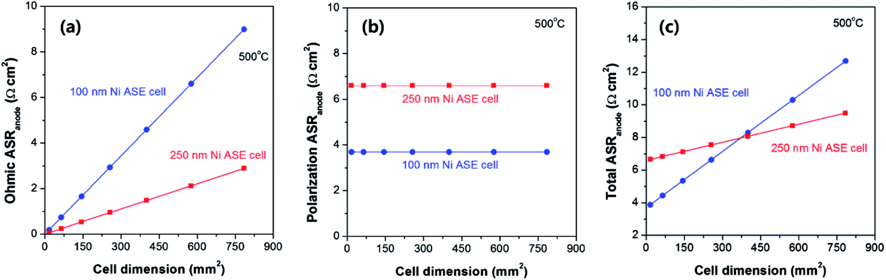 | ||
| Fig. 7 (a) Ohmic, (b) polarization, and (c) total anodic area specific resistances (ASRs) of 100 and 250 nm-thick Ni ASEs according to the cell dimensions, at 500 °C. | ||
4. Conclusions
In this study, we have systematically investigated the morphological, electrical and electrochemical properties of Ni thin-film electrodes supported on an AAO template according to deposition conditions with the goal of realizing a high-performance LT-SOFC. The microstructure, effective electrical conductivity, H2 gas permeability and ohmic and polarization resistances of Ni ASE were greatly influenced by the deposition pressure and film thickness. Furthermore, the ohmic and polarization resistances of the Ni ASE changed in opposite directions depending on its thicknesses. Due to the difficulty in locating the current collector, it was found that as the cell area increased, the smooth current flow in the in-plane direction became even more important in the Ni ASE. Through these observations, we successfully specified the deposition conditions to achieve the optimal electrode performance at the given cell dimensions.Acknowledgements
This work was supported by the Global Frontier R&D Program on Center for Multiscale Energy System funded by the National Research Foundation under the Ministry of Science, ICT & Future, Korea (2011-0031569), and was supported by the Korea Institute of Energy Technology Evaluation and Planning (KETEP) and the Ministry of Trade, Industry & Energy (MOTIE) of the Republic of Korea (20163030031850), and was supported by Basic Science Research Program through the National Research Foundation of Korea (NRF) funded by the Ministry of Education (2016R1A6A3A01013994).Notes and references
- B. C. Steele and A. Heinzel, Nature, 2001, 414, 345–352 CrossRef CAS PubMed.
- A. B. Stambouli and E. Traversa, Renewable Sustainable Energy Rev., 2002, 6, 433–455 CrossRef CAS.
- A. Evans, A. Bieberle-Hütter, J. L. Rupp and L. J. Gauckler, J. Power Sources, 2009, 194, 119–129 CrossRef CAS.
- C.-C. Chao, C.-M. Hsu, Y. Cui and F. B. Prinz, ACS Nano, 2011, 5, 5692–5696 CrossRef CAS PubMed.
- M. Tsuchiya, B.-K. Lai and S. Ramanathan, Nat. Nanotechnol., 2011, 6, 282–286 CrossRef CAS PubMed.
- J. An, Y.-B. Kim, J. Park, T. M. Gür and F. B. Prinz, Nano Lett., 2013, 13, 4551–4555 CrossRef CAS PubMed.
- S. Ji, J. Ha, T. Park, Y. Kim, B. Koo, Y. B. Kim, J. An and S. W. Cha, Int. J. Precis. Eng. Manuf., 2016, 3, 35–39 CrossRef.
- D. Beckel, A. Bieberle-Hütter, A. Harvey, A. Infortuna, U. Muecke, M. Prestat, J. Rupp and L. Gauckler, J. Power Sources, 2007, 173, 325–345 CrossRef CAS.
- S. Kang, P. Su, Y. Park, Y. Saito and F. Prinz, J. Electrochem. Soc., 2006, 153, A554–A559 CrossRef CAS.
- S. Kang, P. Heo, Y. H. Lee, J. Ha, I. Chang and S.-W. Cha, Electrochem. Commun., 2011, 13, 374–377 CrossRef CAS.
- K. Bae, H.-S. Noh, D. Y. Jang, J. Hong, H. Kim, K. J. Yoon, J.-H. Lee, B.-K. Kim, J. H. Shim and J.-W. Son, J. Mater. Chem. A, 2016, 4, 6395–6403 CAS.
- J. H. Joo and G. M. Choi, Solid State Ionics, 2007, 178, 1602–1607 CrossRef CAS.
- S. Ji, I. Chang, Y. H. Lee, J. Park, J. Y. Paek, M. H. Lee and S. W. Cha, Nanoscale Res. Lett., 2013, 8, 1–7 CrossRef PubMed.
- D. Sarantaridis and A. Atkinson, Fuel Cells, 2007, 7, 246–258 CrossRef CAS.
- J.-W. Son and H.-S. Song, Int. J. Precis. Eng. Manuf., 2014, 1, 313–316 CrossRef.
- H. G. Seo, Y. Choi, B. Koo, A. Jang and W. Jung, J. Mater. Chem. A, 2016, 4, 9394–9402 CAS.
- W. Jung, J. J. Kim and H. L. Tuller, J. Power Sources, 2015, 275, 860–865 CrossRef CAS.
- A. Faes, A. Hessler-Wyser and A. Zryd, Membranes, 2012, 2, 585–664 CrossRef CAS PubMed.
- S. Ji, Y. H. Lee, T. Park, G. Y. Cho, S. Noh, Y. Lee, M. Kim, S. Ha, J. An and S. W. Cha, Thin Solid Films, 2015, 591, 250–254 CrossRef CAS.
- S. Noh, G. Y. Cho, Y. H. Lee, W. Yu, J. An and S. W. Cha, Sci. Adv. Mater., 2016, 8, 11–16 CrossRef CAS.
- S. Lee, J. Seo and W. Jung, Nanoscale, 2016, 8, 10219–10228 RSC.
- R. Islamgaliev, R. Y. Murtazin, L. Syutina and R. Valiev, Phys. Status Solidi A, 1992, 129, 231–236 CrossRef CAS.
- G. Sobe, H. Schreiber, G. Weise and A. Heinrich, Contrib. Plasma Phys., 1992, 32, 623–636 CrossRef CAS.
- M. Lee, S. Seo, D. Seo, E. Jeong and I. Yoo, Integr. Ferroelectr., 2004, 68, 19–25 CrossRef CAS.
- K. Chan and B. Teo, IET Sci., Meas. Technol., 2007, 1, 87–90 CrossRef CAS.
- A. Foroughi-Abari, C. Xu and K. C. Cadien, Thin Solid Films, 2012, 520, 1762–1767 CrossRef CAS.
- A. Dirks and H. Leamy, Thin Solid Films, 1977, 47, 219–233 CrossRef CAS.
- Y. Choi, E. C. Brown, S. M. Haile and W. Jung, Nano Energy, 2016, 23, 161–171 CrossRef CAS.
- N. Perry, S. Kim and T. Mason, J. Mater. Sci., 2008, 43, 4684–4692 CrossRef CAS.
- N. W. Kwak and W. Jung, Acta Mater., 2016, 108, 271–278 CrossRef CAS.
Footnotes |
| † Electronic supplementary information (ESI) available. See DOI: 10.1039/c7ra02719b |
| ‡ These two authors made equal contributions. |
| This journal is © The Royal Society of Chemistry 2017 |