
 Open Access Article
 This Open Access Article is licensed under a Creative Commons Attribution-Non Commercial 3.0 Unported Licence
Edge hydrogenation-induced spin-filtering and negative differential resistance effects in zigzag silicene nanoribbons with line defects†
Xiaoteng Li a,
Dongqing Zoua,
Bin Cuia,
Changfeng Fangb,
Jingfen Zhaoa,
Dongmei Li*a and
Desheng Liu*ab
a,
Dongqing Zoua,
Bin Cuia,
Changfeng Fangb,
Jingfen Zhaoa,
Dongmei Li*a and
Desheng Liu*ab
aSchool of Physics, State Key Laboratory of Crystal Materials, Shandong University, Jinan 250100, People's Republic of China. E-mail: liuds@sdu.edu.cn; li_dm@sdu.edu.cn
bDepartment of Physics, Jining University, Qufu 273155, People's Republic of China
First published on 11th May 2017
Abstract
We investigate the effects of line defects (558-defect and 57-defect) and edge hydrogenation (mono-hydrogenation and di-hydrogenation) on magnetism and spin transport of zigzag silicene nanoribbons (ZSiNRs) by first-principles calculations. The line defects and edge hydrogenation are able to tune the edge and interedge spin polarization in the defective ZSiNRs. The ZSiNRs can be formed into antiferromagnetic (AFM)-metals, ferromagnetic (FM)-metals, AFM and FM semiconductors through modulating the line defects and edge hydrogenation. Moreover, the perfect spin-filtering effect (SFE) with 100% spin polarization and negative differential resistance (NDR) effect can be achieved by di-hydrogenation in our proposed devices. Our findings demonstrate that the ZSiNRs with diverse line defects and edge hydrogenation are promising materials for spintronic applications.
1. Introduction
Silicene, a hexagonal network with single atomic layer of silicon, has gained much interest because it shows comparable electronic characteristics to graphene.1–6 For example, a Dirac-fermion-containing, zero-gap semimetal and high Fermi velocity have been discovered in a free-standing sheet of silicene.1,3,4,7,8 Unlike flat graphene, the stable structure of silicene is buckled due to weak π–π overlaps,9 which results in mixed sp2 and sp3 hybridization in silicene. Moreover, owing to its buckled nature, silicene becomes superior than graphene in many aspects, such as having an enhanced quantum Hall effect,7 electrically tunable band-gap3 and better surface reactivity.10 Another obvious advantage of silicene is the better compatibility with current silicon-based technologies.10–12 Very recently, silicene nanosheet has been fabricated successfully on several metallic substrates, such as Ag(111),4 Ir(111),13 Au(110),14 etc. Subsequently, its one-dimensional derivatives, silicene nanoribbons (SiNRs) have also been synthesized by experimenters.15,16 SiNRs has two edge types, i.e., zigzag silicene nanoribbons (ZSiNRs) and armchair silicene nanoribbons (ASiNRs), which is similar to graphene nanoribbons (GNRs). Investigations demonstrate that the ground state of ZSiNRs is antiferromagnetic coupling between the two edges, leading to zero total magnetization.17 This hinders the actual applications of pristine ZSiNRs in spintronic.In order to tune the magnetism and electronic properties of ZSiNRs, many efforts have been devoted to modify spin polarization, such as doping,18,19 edge hydrogenation20–22 and introducing defects.23,24 Defects are often the first concern in the actual application of two-dimensional materials because they can greatly alter the mechanical, electronic, magnetic, and transport properties of pure sheets.25–27 In particular, line defects which could remain structurally stable have been extensively introduced into the graphene lattice. Recently, Tang et al.28 reported the effect of one-dimensional defects, containing octagonal and paired pentagonal sp2-carbon rings (558-defect), on the magnetism of ZGNRs. The results indicate that ZGNRs with 558-defect on one side exhibit long-range ferromagnetic ordering on the other side, and the corresponding spin-filter efficiency could reach 60%. Besides that, another line defect, linkages of a pentagon and a heptagon (57-defect), has also been theoretically introduced into ZGNRs.29 It is concluded that the 558-defect or 57-defect on one edge could facilely tailor the magnetism and electronic properties of ZGNRs. Given that the reconstructed ZGNRs show many excellent properties, the research on magnetic and spin transport features of ZSiNRs with extended defects will also be a meaningful topic. To date several kinds of grain boundaries (GBs) being observed during the synthesis of silicene on Ag(111).30 Therefore, the possibility of finding a controlled manner to modify these GBs to insert different kinds of line defects in SiNRs is hugely increased. Moreover, theoretical investigations have predicted the possibility of existing 558-defect and 57-defect in SiNRs.24,31 While the influence of the extended defects on magnetism, electronic structures and transport properties of ZSiNRs is rarely reported.
What's more, the edges of SiNRs are often chemically modified because the edge dangling bonds of pristine SiNRs are unstable. Edge hydrogenation has been widely employed to tune properties of ZSiNRs.19,20 For example, Ding et al. studies the H-poor and H-rich surroundings have an important influence on electronic structures of ZSiNRs with one Klein edge.21 They also reported that ZSiNRs with asymmetric sp2–sp3 edges exhibit an interesting bipolar magnetic semiconducting behaviour.32 Deng et al. investigate the spin transport of a heterostructure, consisting of semi-hydrogenation ZSiNRs and ZSiNRs.33 The result shows that semi-hydrogenation and full-hydrogenation have different influence on electronic structure of ZSiNRs. Also they report the spin transport features of the Al-doping ZSiNRs with asymmetric edge hydrogenation and perfect spin filtering and rectifying effect can be achieved in such devices.34 In this work, using the first-principles approach, we focus on the impact of the line defects (558-defect and 57-defect) and edge hydrogenation (mono-hydrogenation and di-hydrogenation) on magnetism and spin transport properties of ZSiNRs. The results show that the spin polarization and spin-transport of ZSiNRs can be tuned via the introduction of line defects and edge hydrogenation. And the nearly 100% spin-filter and negative differential resistance (NDR) effect can be observed in our proposed devices.
2. Models and methods
The geometries of ZSiNRs with line defects and edge hydrogenation are presented in Fig. 1(a) and (b), which consist of eight zigzag silicon chains across the width. Two kinds of line defects are considered in the ten ribbons, labeled with M1–M5 for 558-defect and M6–M10 for 57-defect. M1 and M2 (M6 and M7) represent that 558-defect (57-defect) is at the center and edge of the nanoribbons, respectively. And all edge silicon atoms of these four unit cells are passivated by one hydrogen atom (mono-H). M3 and M4 (M8 and M9) represent that one edge of 558-defect (57-defect) ZSiNRs is saturated by two hydrogen atoms (di-H) and the other one is still mono-hydrogenated. M5 and M10 represent both sides of the nanoribbons are passivated by di-H. After geometric optimizations, the Si–Si bond lengths of pentagonal and octagonal rings are within 2.28–2.33 Å for M1, M2 and M3, and 2.22–2.36 Å for M4 and M5 in 558-defect ZSiNRs. In 57-defect ZSiNRs, the Si–Si bond lengths of pentagonal and heptagonal rings are within 2.27–2.39 Å for M6, M7 and M8, and little larger within 2.3–2.42 Å for M9 and M10. Then the two-probe systems are built as depicted in Fig. 1(c). Here we only display the case of the M5 system as an example. The edge energy which determine the stabilities of different edge types is calculated (Table S1, ESI†). It can be concluded that 558-defect (57-defect) ZSiNRs become more and more stable with increasing the number of H atoms.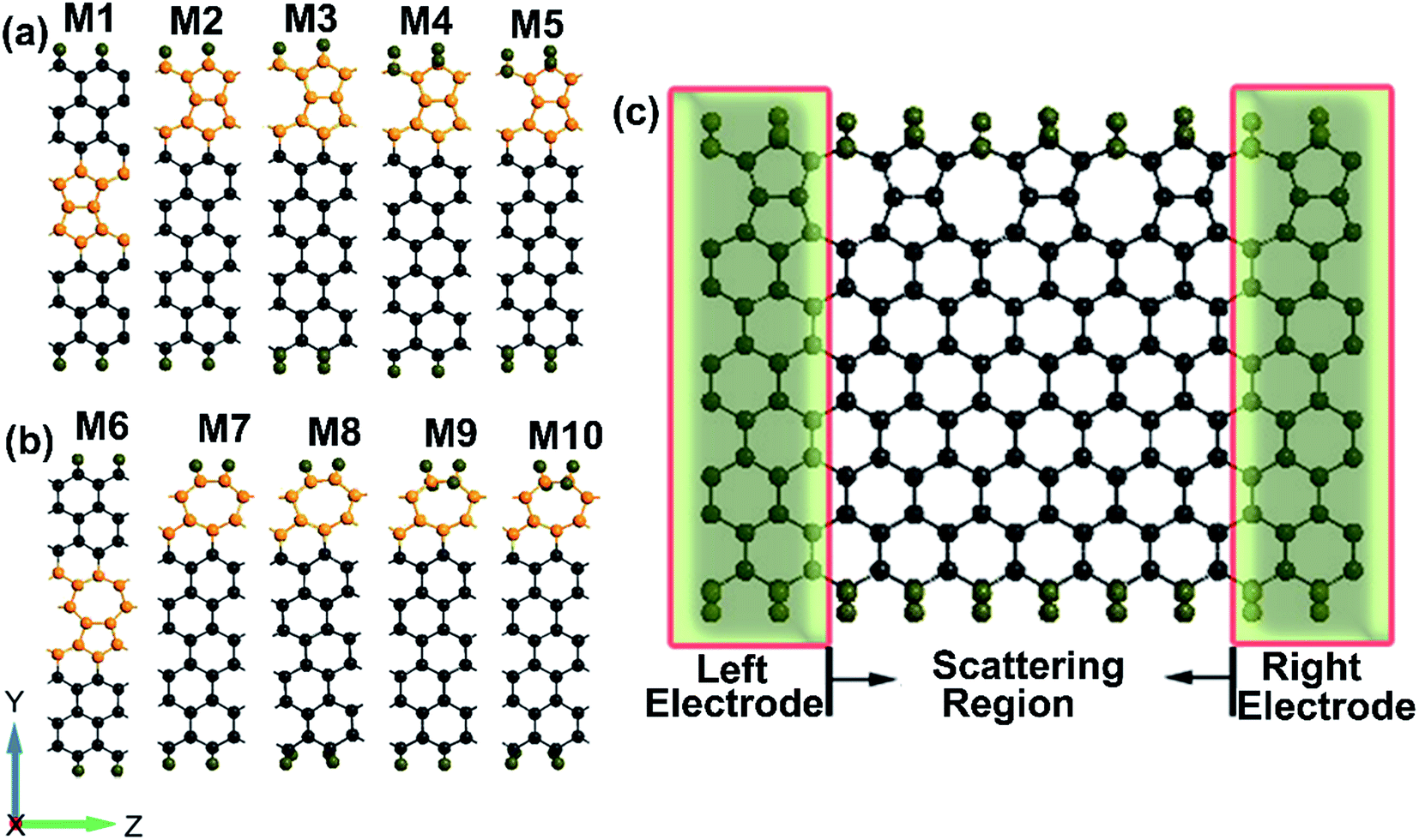 | ||
| Fig. 1 (a) and (b) show ZSiNRs unit cell with extended line defects. M1 and M2 (M6 and M7) correspond to the 558-defect (57-defect) (pictured by orange) located at the center and edge, and the silicon atoms on edges are saturated with mono-H. M3, M4, M8 and M9 correspond to line defects located at one side of the nanoribbons, and all they have one mono-H edge and one di-H edge. M5 and M10 correspond to line defects located at one side, and the edge silicon atoms are saturated with di-H. (c) Schematic view of the two-probe system constituted by M5. | ||
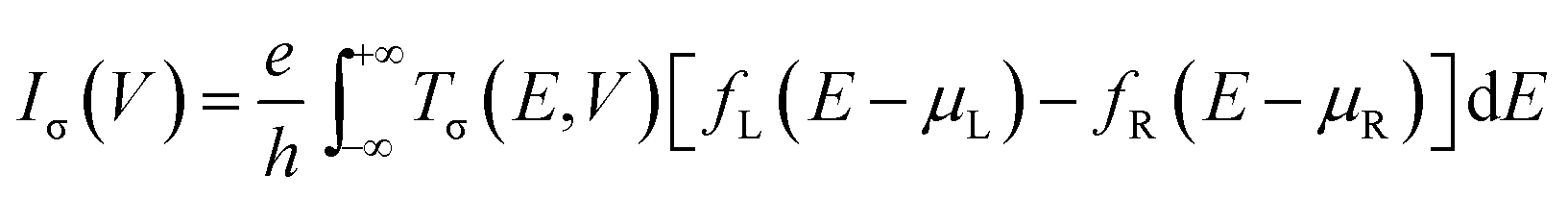
The geometry optimization and electronic properties are calculated by Atomistix ToolKit (ATK 2013.8) package, which is based on the density functional theory (DFT) combined with the non-equilibrium Green's function (NEGF).35–38 The spin-dependent generalized gradient approximation with the Perdew–Burke–Ernzerhof (SGGA-PBE) is employed for the exchange–correlation potential and the double-zeta polarized basis set (DZP) is used for electron wave functions. The structures are relaxed until the atoms forces converge to 0.02 eV Å−1. The spin polarized current Iσ through the central region is evaluated by the Landauer–Büttiker formula:
3. Results and discussion
3.1 The effect of defect position on ZSiNRs terminated by mono-hydrogenation (M1, M2, M6, M7)
For comparison with the ideal ZSiNRs which have the antiferromagnetically coupled state, we firstly calculate the ground energies for the ten defective structures drawn in Fig. 1(a) and (b) under the different initial spin configurations as shown in Table 1. Here, the spin configuration notations are defined to be the coupling between the two ferro-magnetic edge states: (i) ferromagnetic, FM (M5), (ii) antiferromagnetic, AFM (M1, M4 and M6), (iii) no spin polarization, NM (none). Other configurations cannot be clarified directly.| Total energy (eV) | Comparison | |||
|---|---|---|---|---|
| NM | FM | AFM | ||
| M1 | −6151.317 | −6151.373 | −6151.377 | NM > FM > AFM |
| M2 | −6151.481 | −6151.515 | −6151.515 | NM > FM = AFM |
| M3 | −6184.042 | −6184.117 | −6184.117 | NM > FM = AFM |
| M4 | −6184.508 | −6184.556 | −6184.563 | NM > FM > AFM |
| M5 | −6217.052 | −6217.163 | −6217.146 | NM > AFM > FM |
| M6 | −6509.300 | −6509.367 | −6509.368 | NM > FM > AFM |
| M7 | −5792.762 | −5792.793 | −5792.793 | NM > FM = AFM |
| M8 | −5825.391 | −5825.414 | −5825.414 | NM > FM = AFM |
| M9 | −5825.906 | −5825.937 | −5825.937 | NM > FM = AFM |
| M10 | −5858.535 | −5858.582 | −5858.582 | NM > FM = AFM |
To know the spin polarization of defective ZSiNRs with mono-H, we plot the distribution of spin polarization density (SPD) (ρ↑–ρ↓) on their lowest-energy states [see Fig. 2]. Apparently, intense spin polarization mainly occurs at the edge Si atoms in 558- and 57-defect ZSiNRs terminated by mono-hydrogenation. For 558-defect ZSiNRs, the directions of spin polarization of the Si atoms on both edges in M1 are just opposite. Therefore, the ground state of M1 is an antiferromagnetic spin configuration. At the position of 558-defect, atoms Si1, Si2, Si3 and Si4 also appear slight spin polarization, which results in the total magnetic moment Mtot being 0.43 μB. Therefore, introducing 558-defect in the center of ZSiNRs can effectively enhance magnetization. When the 558-defect shifts from the center to the top edge, the edge Si atoms will adopt sp2 hybridization and atoms Si1, Si2, Si3 and Si4 will adopt sp3 hybridization. So the SPD of the top edge will reduce to zero affected by edge mono-hydrogenation. Due to the ferromagnetic ordering of the Si atoms on the bottom edge, the ground state of M2 corresponds to FM configuration with a 0.69 μB magnetic moment. There is an analogous phenomenon in 57-defect ZSiNRs. When the line defect locates in the center, the ground state of M6 is an AFM spin configuration and the total net spin is zero. After the 57-defect moves to the top edge, the Si atoms on the top edge are spin-nonpolarized and those on the bottom edge are ferromagnetic coupling. Thus M7 exhibits FM configuration, Mtot = 0.61 μB. It suggests that the 57-defect has an obvious inhibitory effect on the spin polarization in ZSiNRs. And both 558- and 57-defect ZSiNRs with mono-H can be tuned from AFM to FM state via changing the line-defect position from the center to the edge.
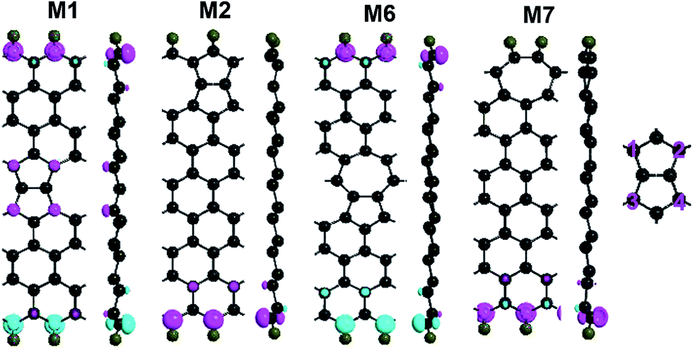 | ||
| Fig. 2 Top and cross views of spin polarization density (ρ↑–ρ↓) at the ground state for M1, M2, M6 and M7, respectively. The isosurface level is 0.02 (Å−3 eV−1). Purple numbers 1, 2, 3 and 4 represent four Si atoms of the 558-defect, denoted by Si1, Si2, Si3 and Si4, respectively. | ||
Then we explore the electronic band structures of the four systems at the ground state as shown in Fig. 3. From the band structures of 558-defect ZSiNRs indicated in M1 and M2, the spin degeneracy is lifted at the Fermi level and there is no band gap for either spin-up or spin-down, thus both M1 and M2 are evidently in metallic states. For 57-defect ZSiNRs, the energy bands of spin-up and spin-down in M6 are nearly degenerate, while those of M7 are spin-splitting near the Fermi level. It can be concluded that the spin polarization is intensified with the 57-defect moving from the center to edge. Moreover, there are no band gaps in M7 and almost zero band gaps in M6 for the two spin channels, so M6 and M7 are in metallic states.
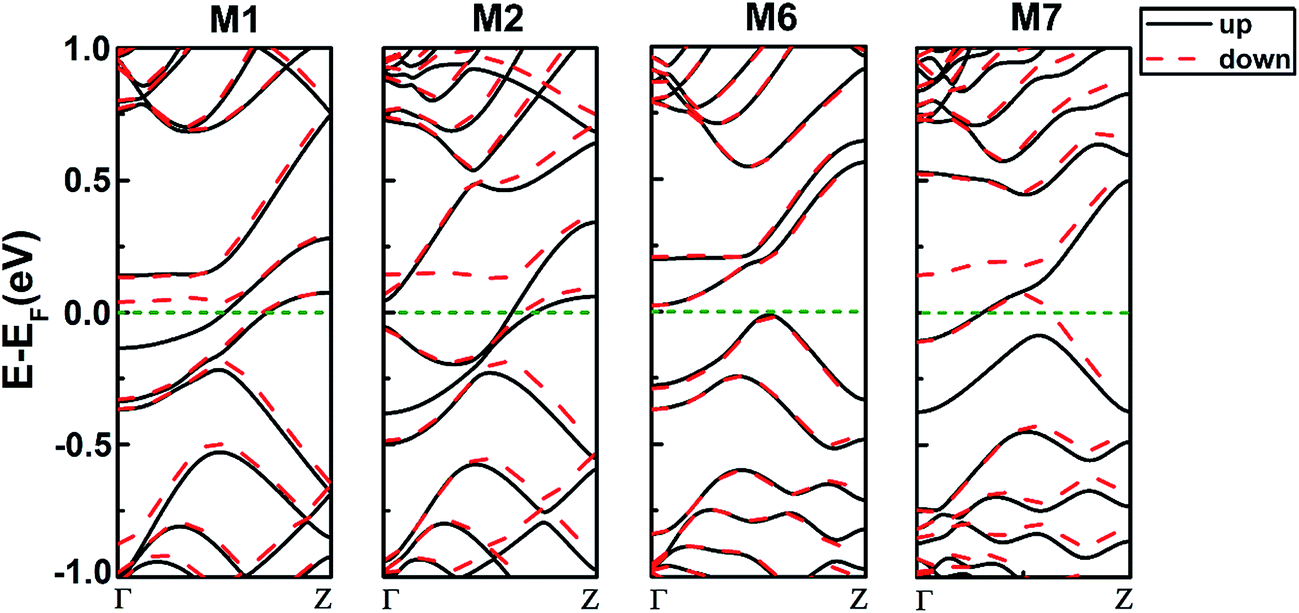 | ||
| Fig. 3 Spin polarized band structures at the ground state for M1, M2, M6 and M7 (spin up, black solid line; spin down, red short dashed line). | ||
3.2 The effect of edge hydrogenation on defective ZSiNRs (M3–M5, M8–M10)
Furthermore, we explore the magnetism of the 558- and 57-defect ZSiNRs with various edge-hydrogenation in M3–M5 and M8–M10 systems, illustrated in Fig. 1(a) and (b). It reveals that the combination of different types of edge-hydrogenation could give rise to diverse magnetic states for the defective ZSiNRs. Seeing from the comparison of the total energy [Table 1], the favorable magnetic state is FM for M5, AFM for M6 but not confirmed for M7–M10. Then Fig. 4 depicts the SPD on the lowest-energy states of the defective nanoribbons with different edge hydrogenation. As far as we know, edge silicon atoms passivated regularly by one H atom will adopt sp2 hybridization, while ones passivated doubly prefer sp3 hybridization. When the Si atoms are sp3 hybridized, the pz orbitals will deep in the valence bands. And the pz orbitals of Si atoms next to edge ones will contribute to magnetic properties.32 For 558-defect ZSiNRs, it clearly shows that intense spin polarization occurs at the edge or interedge Si atoms. In M3, the defect edge is passivated by mono-H, so the edge Si atoms adopt sp2 hybridization and the atoms Si1 and Si2 adopt sp3 hybridization. It results in atoms of 558-defect on the top edge being spin-nonpolarized. The zigzag edge of M3 is passivated by di-H, so the interedge Si atoms are sp2 hybridized. The zigzag edge is ferromagnetically coupling, causing M3 being FM configuration with Mtot = 1.14 μB. In M4, when the defect edge is passivated by di-H, the atoms Si1 and Si2 are sp2 hybridized. So the spin polarization on the position of 558-defect appears again. The directions of spin polarization on both edges are just inverse, so M4 corresponds to AFM configuration. When both edges of the nanoribbons are di-hydrogenated, just as M5, the interedge Si atoms on two sides show intense spin polarization. And the spin polarized directions are consistent, leading to the FM configuration for M5, Mtot = 1.90 μB. It suggests that the 558-defect ZSiNRs with di-hydrogenated edges have the strongest spin polarization effect. What's more, comparing the SPD of M1–M5, it can be concluded that 558-defect can effectively intensify spin polarization in ZSiNRs but it subjects to the constraint of edge hydrogenation. For 57-defect ZSiNRs, it can be seen that intense spin polarization only occurs on the zigzag edge because 57-defect has an inhibitory effect on the spin polarization. The zigzag edge is di-hydrogenated for M8 and M10 and mono-hydrogenated for M9. Therefore, the interedge Si atoms of M8 and M10 and the edge Si atoms of M9 are sp2 hybridized. All the three systems are ferromagnetically coupling on zigzag edge. Consequently, the ground states of M8, M9 and M10 correspond to FM configurations and their total magnetic moment are 0.78, 0.77 and 1.00 μB. Comparing M6–M10, it can be found that when the 57-defect is on one edge in ZSiNRs, the ground state will prefer FM configuration no matter what types of hydrogenation the edges are.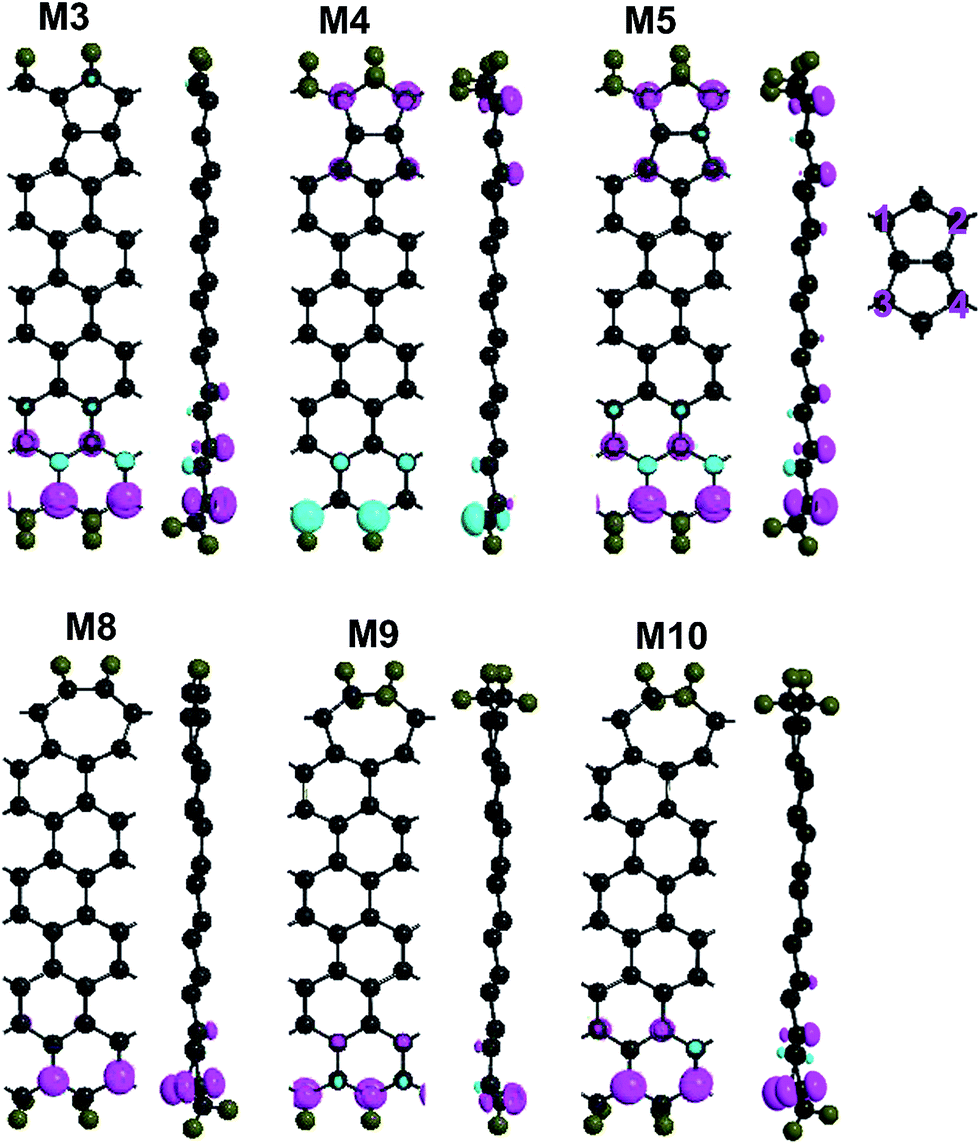 | ||
| Fig. 4 Top and cross views of spin polarization density (ρ↑–ρ↓) at the ground state for M3–M5, M8–M10, respectively. The isosurface level is 0.02 (Å−3 eV−1). Purple numbers 1, 2, 3 and 4 represent four Si atoms of 558-defect, denoted by Si1, Si2, Si3 and Si4, respectively. | ||
The electronic band structures of M3–M5 and M8–M10 for both spin channels at the ground states are shown in Fig. 5. The energy bands at the Fermi level mainly determined by the edge Si atoms on mono-hydrogenated edges and the interedge Si atoms on di-hydrogenated edges. From the band structures of 558-defect ZSiNRs indicated in M3–M5, we can notice that all the three systems are spin polarized, especially more obviously for M5. It indicates that the system that both edges are saturated with di-H has the strongest spin polarization in 558-defect ZSiNRs. And the spin-filter effect in the devices constructed by M3–M5 will be more intense than that in the devices constructed by M1 and M2. Moreover, intense spin polarization creates band gaps for both spin channels, about 0.25 and 0.2 eV energy gaps for M4 and 0.48 and 0.40 eV energy gaps for M5. It means that 558-defect ZSiNRs can be changed from an initial metallic state to a semiconductor state by adjusting edge hydrogenation. In addition, the whole bottom conduction and top valence bands in M5 belong to different spin channels completely, that reveals a typical bipolar character for spintronic applications.39 From the band structures of 57-defect ZSiNRs as displayed in M8–M10, it can be viewed that the energy bands of spin-up and spin-down in M8–M10 split obviously. It suggests the intense spin polarization occurs when 57-defect ZSiNRs are hydrogenated by two H atoms. And some bands get across the Fermi level in these systems which implies that M8–M10 are all ferromagnetic metals. In general, the defective ZSiNRs can be transformed to antiferromagnetic semiconductors, ferromagnetic semiconductors and ferromagnetic metals through modulating edge hydrogenation.
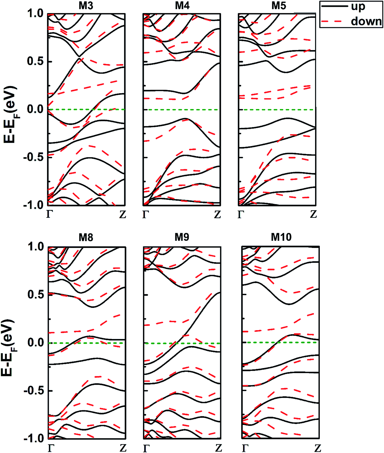 | ||
| Fig. 5 The spin polarized band structures of 558-defect ZSiNRs with different hydrogenated edges, i.e. M3–M5; 57-defect ZSiNRs with different hydrogenated edges, i.e. M8–M10. | ||
3.3 Spin transport properties in defective ZSiNRs with different edge hydrogenation (devices constructed by M3–M5 and M8–M10)
We next turn to study spin transport properties of devices structured by M3–M5 and M8–M10 plotted in Fig. 1(c). The spin-resolved current–voltage (I–V) curves are presented in Fig. 6(a). For 558-defect ZSiNRs, in M4 and M5 devices, the currents of spin-up and spin-down are almost completely suppressed under small voltages and then increase quickly. It presents a typical semiconductor characteristic and the threshold voltages of both spins are about 0.2 V, 0.2 V for M4 and 0.4 V, 0.5 V for M5, as shown in the first-row panels of Fig. 6(a). In M3, the I–V curves of spin-up and spin-down increase with voltage rapidly before 0.5 V and then drop slightly. The spin polarization of M3 and M4 is much weaker than that of M5. This can be quantified directly by the spin filtering efficiency (SFE) as a function of bias voltage in Fig. 6(b). SFE is defined in terms of the spin-resolved current: SFE = (Iup − Idown)/(Iup + Idown), where Iup/down represents the spin-up/spin-down current at finite bias. The value of SFE is about 100% at 0.2 V and −90% at 0.4 and 0.5 V in M5. It indicates that device M5 is a potential candidate for the dual-direction spin filters. For 57-defect ZSiNRs, in device M8, an intriguing spin negative differential resistance (NDR) develops in the bias range 0.1–0.3 V for spin-up electrons and 0.3–0.4 V for spin-down electrons. The spin-up (spin-down) current reaches a maximum at 0.1 (0.3) V and then decreases significantly to a minimum at 0.3 (0.4) V before it increases again. Besides, the spin-filter in M8 is quite excellent and the SFE could maintain 60–100% as 0.15 ≤ Vb ≤ 0.4 V. In device M9, the current of spin-up increases quickly and keeps larger than that of spin-down. On the contrary, the spin-down current always remains higher than the spin-up current in device M10. The peak values of SFE in M9 and M10 are about 60% and −50%, respectively. In conclusion, edge hydrogenation plays a notable role in improving SFE for 558- and 57-defect ZSiNRs. And our proposed all-silicon devices can present multiple high-performance spin-dependent transport properties.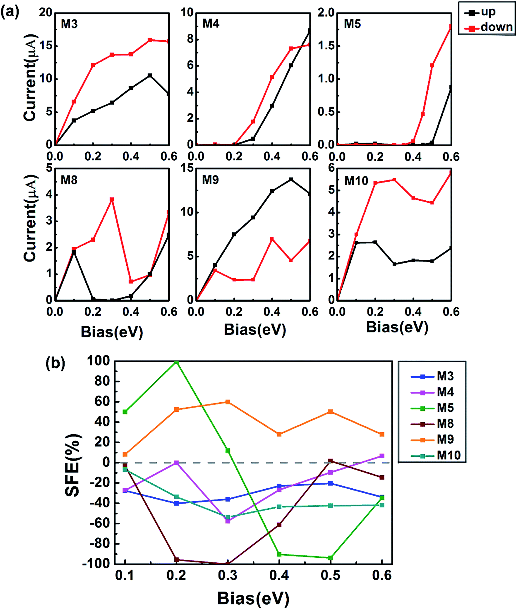 | ||
| Fig. 6 (a) The spin-resolved current–voltage characteristics of defective ZSiNRs with different hydrogenation. (b) The corresponding SFE of M3–M5 and M8–M10. | ||
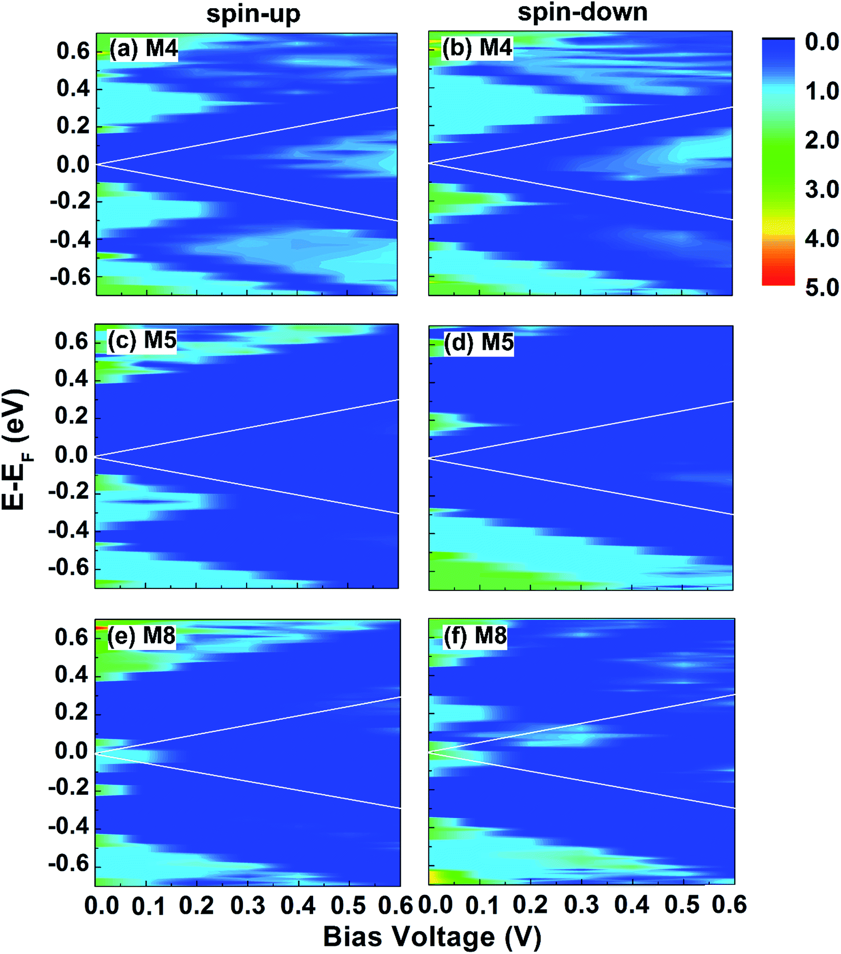
To gain a better understanding of the transport properties of these several systems, we plot 3D contour plots of the spin-up and spin-down transmission spectra versus the applied bias voltage and the electron energy in Fig. 7 for devices M4, M5 and M8. The two white solid lines in each panel indicate the transport window in which the transmission contributes to the currents. In M4 system, the electrons of opposite spins behave in the similar way. There are conductance gaps of width 0.25 and 0.2 eV at EF under zero bias for both spins corresponding to the band gaps of M4. After the bias higher than the threshold voltage 0.2 V, a central transmission spectrum emerges in both channels and the currents begin to increase with voltage as shown in Fig. 7(a) and (b). Similarly in M5 system, large conductance gaps of width 0.48 and 0.4 eV occurs at EF under zero bias [see Fig. 7(c) and (d)]. And the conductance gaps are always wider than the transport window at low bias. Therefore, the spin-up and spin-down currents are almost entirely suppressed at low bias. Not until 0.6 V for up channel and 0.5 V for down channel does the weak transmission peak appears. Since the spin-up transmission is always weaker than the spin-down transmission in the bias window after 0.3 V, so the spin-up current through the system is much smaller than the spin-down current. Especially at 0.5 V, the spin-down channel has been opened but the spin-up channel is still blocked, resulting in the SFE up to 96%. The NDR effect appears in M8 system is explained in Fig. 7(e) and (f). There are obvious peaks in transmission spectra at EF under zero bias for both spins. And the transmission integration increases gradually under low voltage. For spin-up electrons, when the voltage increases to 0.2 V, a large conductance gap appears because of the mismatch of spin-up energy bands. Therefore, the spin-up current increases from 0 to 0.1 V and then decreases to zero at 0.3 V. As a result, the NDR occurs. For spin-down electrons, the transmission does not decrease until the bias is higher than 0.3 V. So the spin-down current increases from 0 to 0.3 V and then decreases to the minimum at 0.4 V. And the NDR occurs. In other words, the NDR occurs for both spin-up and spin-down electrons in M8. Moreover, the transmission of spin-down is much larger than that of spin-up, especially between 0.2 and 0.3 V where the spin-up transport is completely suppressed. As a consequence, the fantastic spin-filtering behavior appears and the SFE is up to nearly 100% in device M8.
 | ||
| Fig. 7 Spin-up, (a), (c) and (e), and spin-down, (b), (d) and (f), transmission spectra as functions of the electron energy and the applied bias voltage for samples M4, M5 and M8. The region between the two white solid lines is referred to as the transport window. | ||
Fig. 8 depicts the spin-resolved transmission spectra at several voltages for devices M3, M9 and M10. It clearly shows that the transmission spectra at zero bias are conducive to transport in the three systems. In M3 and M10, the integration of the spin-down transmission function in the transport window is always larger than that of the spin-up transmission function, but just opposite in M9. Therefore, the spin-down current is always larger than the spin-up current in M3 and M10, and M9 is inverse. In the case of 0.2 V in M3, the obvious difference between spin-up and spin-down transmission results in the SFE up to a maximum nearly 40%. In M9, there is a large conductance gap in the energy region [−0.1, 0.06 eV] for spin down electrons but an obvious transmission platform in [−0.1, 0.15 eV] for spin up electrons at 0.3 V, shown in Fig. 8(b). Therefore, the SFE of M9 reaches a maximum about 60% at 0.3 V. A similar phenomenon can also be observed from the transmission spectra in M10 as shown in Fig. 8(c). And the SFE of M10 achieves a peak value about 50% at 0.3 V. Furthermore, the electron transmission pathways in central region of M3, M9 and M10 are plotted in Fig. S1.† It can be seen that the spin-up and spin-down electrons of M3 at 0 eV energy with 0.2 V transmit mainly via the upper edge of the nanoribbons. For M9, the spin-up electrons at EF with 0.3 V could transmit through the up and down edges [Fig. S1(c), ESI†], but the spin-down channel is blocked completely. For M10, the transmission pathways of spin-down electrons at 0.1 eV with 0.3 V mainly go along the top edge of the nanoribbon as shown in Fig. S1(d),† and the spin-up channel is suppressed.
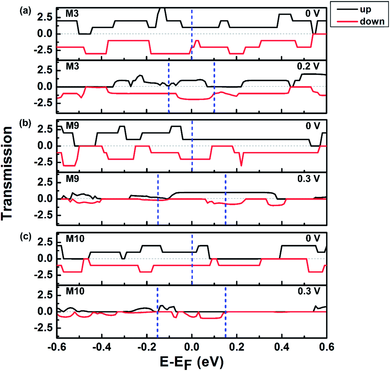 | ||
| Fig. 8 Spin-dependent transmission spectra for (a) M3, (b) M9. (c) M10 at several voltages. The region between the two blue dash lines is referred to as the transport window. | ||
4. Conclusions
In conclusion, employing the density functional theory combined with the non-equilibrium Green's function method, we have investigated the electronic structure, magnetism and spin transport properties of ZSiNRs with line defects (558- and 57-defect) and edge hydrogenation. When 558-defect (57-defect) is introduced in ZSiNRs with mono-H, the edge silicon atoms exhibit intense spin polarization. And the defective ZSiNRs can realize a transition from AFM to FM via varying the position of line defects from the center to the edge. Moreover, the introduction of 558-defect in ZSiNRs can effectively enhance the spin polarization of the nanoribbons. Then we consider the effect of edge hydrogenation on the properties of the defective ZSiNRs. When the edge is di-hydrogenated, the interedge silicon atoms exhibit intense spin polarization. For 558-defect ZSiNRs, the ground state can be tuned from an initial FM metallic state to a FM semiconductor and an AFM semiconductor by adjusting mono- or di-hydrogenation. But for 57-defect ZSiNRs, the ground state always remains a FM metallic state in these systems with different kinds of edge hydrogenation. In addition, the spin-transport of the defective ZSiNRs with various edge hydrogenation is studied. The NDR is predicted for both spins in the device constructed by the 57-defect ZSiNRs with one mono-hydrogenated 57-defect edge and one di-hydrogenated zigzag edge. The perfect spin-filter effect is also observed in these devices. It can be concluded that edge hydrogenation has an important impact on the spin polarization and spin-transport of 558- and 57-defect ZSiNRs. These results may be useful for the fabrication of high performance spin-related devices based on silicene nanospintronics.Acknowledgements
This work was supported by the Natural Science Foundation of China (Grant No. 11374183, 11574118, 21473102, 11404141 and 11404188).References
- S. Cahangirov, M. Topsakal, E. Aktürk, H. Şahin and S. Ciraci, Phys. Rev. Lett., 2009, 102, 236804 CrossRef CAS PubMed.
- M. E. Dávila, A. Marele, P. D. Padova, I. Montero, F. Hennies, A. Pietzsch, M. N. Shariati, J. M. Gómez-Rodríguez and G. L. Lay, Nanotechnology, 2012, 23, 385703 CrossRef PubMed.
- Z. Ni, Q. Liu, K. Tang, J. Zheng, J. Zhou, R. Qin, Z. Gao, D. Yu and J. Lu, Nano Lett., 2012, 12, 113–118 CrossRef CAS PubMed.
- P. Vogt, P. De Padova, C. Quaresima, J. Avila, E. Frantzeskakis, M. C. Asensio, A. Resta, B. Ealet and G. Le Lay, Phys. Rev. Lett., 2012, 108, 155501 CrossRef PubMed.
- K. S. Novoselov, A. K. Geim, S. V. Morozov, D. Jiang, M. I. Katsnelson, I. V. Grigorieva, S. V. Dubonos and A. A. Firsov, Nature, 2005, 438, 197–200 CrossRef CAS PubMed.
- K. S. Novoselov, A. K. Geim, S. V. Morozov, D. Jiang, Y. Zhang, S. V. Dubonos, I. V. Grigorieva and A. A. Firsov, Science, 2004, 306, 666–669 CrossRef CAS PubMed.
- C.-C. Liu, W. Feng and Y. Yao, Phys. Rev. Lett., 2011, 107, 076802 CrossRef PubMed.
- L. Chen, C. C. Liu, B. Feng, X. He, P. Cheng, Z. Ding, S. Meng, Y. Yao and K. Wu, Phys. Rev. Lett., 2012, 109, 056804 CrossRef PubMed.
- G. G. Guzmán-Verri and L. C. Lew Yan Voon, Phys. Rev. B: Condens. Matter Mater. Phys., 2007, 76, 075131 CrossRef.
- H. Sahin and F. M. Peeters, Phys. Rev. B: Condens. Matter Mater. Phys., 2013, 87, 085423 CrossRef.
- A. Kara, H. Enriquez, A. P. Seitsonen, L. C. Lew Yan Voon, S. Vizzini, B. Aufray and H. Oughaddou, Surf. Sci. Rep., 2012, 67, 1–18 CrossRef CAS.
- J. Sivek, H. Sahin, B. Partoens and F. M. Peeters, Phys. Rev. B: Condens. Matter Mater. Phys., 2013, 87, 085444 CrossRef.
- L. Meng, Y. Wang, L. Zhang, S. Du, R. Wu, L. Li, Y. Zhang, G. Li, H. Zhou, W. A. Hofer and H. J. Gao, Nano Lett., 2013, 13, 685–690 CrossRef CAS PubMed.
- M. Rachid Tchalala, H. Enriquez, A. J. Mayne, A. Kara, S. Roth, M. G. Silly, A. Bendounan, F. Sirotti, T. Greber, B. Aufray, G. Dujardin, M. Ait Ali and H. Oughaddou, Appl. Phys. Lett., 2013, 102, 083107 CrossRef.
- P. De Padova, P. Perfetti, B. Olivieri, C. Quaresima, C. Ottaviani and G. Le Lay, J. Phys.: Condens. Matter, 2012, 24, 223001 CrossRef PubMed.
- P. De Padova, O. Kubo, B. Olivieri, C. Quaresima, T. Nakayama, M. Aono and G. Le Lay, Nano Lett., 2012, 12, 5500–5503 CrossRef CAS PubMed.
- Y. Ding and J. Ni, Appl. Phys. Lett., 2009, 95, 083115 CrossRef.
- H.-X. Luan, C.-W. Zhang, F.-B. Zheng and P.-J. Wang, J. Phys. Chem. C, 2013, 117, 13620–13626 CAS.
- D.-Q. Fang, S.-L. Zhang and H. Xu, RSC Adv., 2013, 3, 24075 RSC.
- X. F. Yang, Y. S. Liu, J. F. Feng, X. F. Wang, C. W. Zhang and F. Chi, J. Appl. Phys., 2014, 116, 124312 CrossRef.
- Y. Ding and Y. Wang, Appl. Phys. Lett., 2014, 104, 083111 CrossRef.
- D. Zou, W. Zhao, C. Fang, B. Cui and D. Liu, Phys. Chem. Chem. Phys., 2016, 18, 11513–11519 RSC.
- R.-L. An, X.-F. Wang, P. Vasilopoulos, Y.-S. Liu, A.-B. Chen, Y.-J. Dong and M.-X. Zhai, J. Phys. Chem. C, 2014, 118, 21339–21346 CAS.
- D. Ghosh, P. Parida and S. K. Pati, Phys. Rev. B: Condens. Matter Mater. Phys., 2015, 92, 195136 CrossRef.
- J. Červenka, M. I. Katsnelson and C. F. J. Flipse, Nat. Phys., 2009, 5, 840–844 CrossRef.
- F. Hao, D. Fang and Z. Xu, Appl. Phys. Lett., 2011, 99, 041901 CrossRef.
- R. R. Nair, M. Sepioni, I. L. Tsai, O. Lehtinen, J. Keinonen, A. V. Krasheninnikov, T. Thomson, A. K. Geim and I. V. Grigorieva, Nat. Phys., 2012, 8, 199–202 CrossRef CAS.
- G. P. Tang, Z. H. Zhang, X. Q. Deng, Z. Q. Fan and H. L. Zhu, Phys. Chem. Chem. Phys., 2015, 17, 638–643 RSC.
- D. Zou, B. Cui, C. Fang, W. Zhao, X. Kong, D. Li, M. Zhao and D. Liu, Org. Electron., 2015, 27, 212–220 CrossRef CAS.
- D. Chiappe, C. Grazianetti, G. Tallarida, M. Fanciulli and A. Molle, Adv. Mater., 2012, 24, 5088–5093 CrossRef CAS PubMed.
- S. Li, Y. Wu, Y. Tu, Y. Wang, T. Jiang, W. Liu and Y. Zhao, Sci. Rep., 2015, 5, 7881 CrossRef PubMed.
- Y. Ding and Y. Wang, Appl. Phys. Lett., 2013, 102, 143115 CrossRef.
- X. Q. Deng, Z. H. Zhang, G. P. Tang, Z. Q. Fan, L. Sun, C. X. Li and H. L. Zhang, Org. Electron., 2016, 37, 245–251 CrossRef CAS.
- X. Q. Deng, Z. H. Zhang, Z. Q. Fan, G. P. Tang, L. Sun and C. X. Li, Org. Electron., 2016, 32, 41–46 CrossRef CAS.
- M. Brandbyge, J.-L. Mozos, P. Ordejón, J. Taylor and K. Stokbro, Phys. Rev. B: Condens. Matter Mater. Phys., 2002, 65, 165401 CrossRef.
- M. S. José, A. Emilio, D. G. Julian, G. Alberto, J. Javier, O. Pablo and S.-P. Daniel, J. Phys.: Condens. Matter, 2002, 14, 2745 CrossRef.
- J. Taylor, H. Guo and J. Wang, Phys. Rev. B: Condens. Matter Mater. Phys., 2001, 63, 245407 CrossRef.
- J. Taylor, H. Guo and J. Wang, Phys. Rev. B: Condens. Matter Mater. Phys., 2001, 63, 121104 CrossRef.
- X. Li, X. Wu, Z. Li, J. Yang and J. G. Hou, Nanoscale, 2012, 4, 5680–5685 RSC.
Footnote |
| † Electronic supplementary information (ESI) available. See DOI: 10.1039/c7ra02624b |
| This journal is © The Royal Society of Chemistry 2017 |